
Highly efficient, large area, roll coated flexible and rigid OPV modules with geometric fill factors up to 98.5% processed with commercially available materials†
L.
Lucera
*a,
F.
Machui
a,
P.
Kubis
a,
H. D.
Schmidt
a,
J.
Adams
a,
S.
Strohm
a,
T.
Ahmad
a,
K.
Forberich
b,
H.-J.
Egelhaaf
*a and
C. J.
Brabec
ab
aZAE Bayern – Solar Factory of the Future, Energy Campus Nürnberg, Fürtherstrasse 250, 90429 Nürnberg, Germany. E-mail: luca.lucera@zae-bayern.de; hans-joachim.egelhaaf@zae-bayern.de
bInstitute of Materials for Electronics and Energy Technology, Friedrich-Alexander Universität Elrangen-Nürnberg, 91058 Erlangen, Germany
First published on 11th November 2015
Abstract
Highly efficient, large area OPV modules achieving full area efficiencies of up to 93% of the reference small area cells are reported. The way to a no-loss up-scaling process is highlighted: photoelectrical conversion efficiencies of 5.3% are achieved on rigid modules and of 4.2% on flexible, roll coated ones, employing a commercially available photoactive material. Exceptionally high geometric fill factors (98.5%), achieved via structuring by ultrashort laser pulses, with interconnection widths below 100 μm are demonstrated.
Broader contextThe achievement of high performances for solar modules can be considered one of the biggest challenges to be tackled in order to make printed photovoltaics suitable for industrial production and commercialization. Often the scientific community is solely focused on achieving the highest, record performances on small scale devices, disregarding the development of suitable up-scaling strategies to minimize the performance drop between single cells and modules. In this contribution the key factors for an ideal large area processing are addressed: optical and electrical simulations for the design of the geometry of the modules and the choice of the electrode materials; roll-to-roll printing and laser structuring demonstrating that losses between cells and modules can be as low as 7%. The use of halogen-free formulations and materials available in large quantities constitute as well an important step towards industrially sustainable processes. |
1. Introduction
In recent years, printable photovoltaic technologies have been attracting the attention of the scientific community, due to their potentialities; in fact, solution processability constitutes a major advantage towards large scale, cheap, industrial production of solar cells. Furthermore, the rapid energy payback time of these technologies makes them of particular interest.1 Despite the high efficiencies reported on lab scale devices, which recently surpassed 10% power conversion efficiency (PCE) for organic photovoltaics (OPV)2 and 20%3 for perovskite based ones, very little progress is shown towards up-scaling processing of solar cells.4–8 Large area, roll-to-roll (R2R) processed solar cells and modules usually show a quite remarkable drop in efficiencies compared to small area, lab-produced hero cells,9 highlighting the importance of the development of a stable, reliable production process which should allow a minimization of the performance losses. Recently we showed what are the guidelines for an optimal upscaling route for large area modules,10 using a combination of optical simulations (transfer matrix formalism – TMF) and electrical simulations (finite element simulations – FEM): a loss in PCE of less than 10% should be achievable for opaque devices under optimized conditions. Generally this involves (i) a careful choice and optimization of the printing techniques, (ii) the development of halogen-free formulations allowing the achievement of the right morphology for the active layers, (iii) the development of a reliable, fast, high resolution patterning method for the monolithical interconnection of the cells in a module, the latest being of particular importance to minimize the size of the interconnection area which is not photoactive and thus is accountable as a loss. The ratio between the photoactive area and the total area of the module is usually referred to as the geometric fill factor (GFF).In this report we performed optical simulations to quantify the losses induced by the change of electrode materials when going to up-scaled modules and compared them with experimental results. Then electrical simulations are carried out to assess the losses due to the monolithic interconnection of the cells in a module and are able to minimize them by choosing the appropriate layout. We will show how theoretical calculations can be matched with experimental results, yielding large area modules with PCEs of up to 90% of the reference hero cells by choosing high precision slot-die coating on a fully R2R compatible printing setup in combination with high precision, ultra-fast laser structuring. Exceptionally high GFF, higher than 98%, with an interconnection width of less than 90 μm are obtained for the first time in the literature.
The relevance of the findings for the community is strengthened by the use of commercially available materials, showing that high PCEs are within reach for a technology which can be defined mature for industrialization.
2. Materials and methods
2.1 OPV devices processing
Inverted structure OPV devices were processed and characterized under ambient conditions. The sequence of layers was electrode1/ZnO nanoparticles/PBTZT-stat-BDTT-8:11 phenyl-C61-butyric acid methyl ester (PCBM)/poly(3,4-ethylenedioxythiophene):polystyrene sulfonate (PEDOT:PSS)/Ag. Reference cells were processed on a indium-tin oxide (ITO) coated glass (electrode 1, 20 Ω sq−1, OSRAM), laser patterned with a laser fluence of 0.55 J cm−2 and 90% overlap at first harmonic wavelength (520 nm) to achieve electrical insulation of the electrode (P1). Large area modules were processed on fluorine-tin oxide (FTO) coated glass substrates (electrode 1, 8 Ω sq−1, Pilkington) and on flexible ITO-Metal-ITO (IMI) sputtered polyethylene terephthalate (PET) substrates (electrode 1, 8 Ω sq−1, Materion). IMI and FTO were laser patterned to achieve P1 with a fluence of 0.41 J cm−2, 50% overlap and 0.9 J cm−2, 98% overlap respectively. After patterning, the glass substrates were subsequently cleaned in an ultrasonic bath in acetone and isopropyl alcohol for 10 min each. Flexible substrates were instead wiped and rinsed with isopropyl alcohol alone. All layers were processed via doctor blading for glass based devices and via slot-die coating for the flexible ones. Slot-die coating was performed using a 10 cm wide heatable slot-die head, mounted on a mini-roll coater (FOM technologies, Denmark). Coating was performed on a heatable backing roll. The parameters changed were wet film thickness of the layer (W), coating speed (v) and temperature of the roll (T). ZnO nanoparticles dispersed in isopropyl alcohol (Nanograde AG) were coated via doctor blading on glass substrates and via slot-die coating on flexible substrates (W = 5 μm, v = 1 m min−1, T = 40 °C), optimizing coating and drying conditions to achieve a film thickness of 50 nm. The layer was dried at 80 °C in a convection oven for 90 s. PBTZT-stat-BDTT-8 from the Lisicon® series was purchased from Merck Chemicals Ltd, Germany and PCBM (technical grade 99%) from Solenne BV, The Netherlands, and dissolved at a concentration of 35 mg ml−1 in a volume ratio 1![[thin space (1/6-em)]](https://www.rsc.org/images/entities/char_2009.gif) :1.5 in o-xylene: tetrahydronaphthalene (9:1) and stirred for 3 h at 90 °C before coating. The photoactive layer (PAL) was then coated in air via doctor blading on glass substrates and via slot die coating on flexible substrates (W = 9.4 μm, v = 2 m min−1, T = 70 °C) aiming at a dried film thickness of 220 nm. The film thickness was optimized through optical density measurements (Fig. S1, ESI†). PEDOT:PSS (Clevios P VP Al4083) from Heraeus Germany was diluted in isopropyl alcohol (1:5 volume ratio) before deposition on glass substrates, obtaining a 50 nm thick layer. PEDOT:PSS (HTL Solar) from Heraeus Germany was diluted in de-ionized water (1:1 volume ratio) and then coated via slot-die coating (W = 10 μm, v = 1 m min−1, T = 40 °C) on flexible substrates, aiming at a dried film thickness of 100 nm. The substrates were then annealed at 120 °C for 5 min in a convection oven and afterwards patterned to remove the coated stack (ZnO/PAL/PEDOT:PSS) to achieve P2 (fluence of 0.27 J cm−2, 93% overlap for FTO based modules and fluence of 0.1 J cm−2, 94% overlap, 3 times repeated for IMI based modules). The devices were completed by thermal evaporation of a thin Ag layer (electrode 2) through a shadowing mask for single devices (100 nm) and full area for modules (250 nm) and then patterned to achieve electrical separation (P3 – fluence of 1.25 J cm−2 and 66% overlap). The layout used for the modules was reported elsewhere.12
:1.5 in o-xylene: tetrahydronaphthalene (9:1) and stirred for 3 h at 90 °C before coating. The photoactive layer (PAL) was then coated in air via doctor blading on glass substrates and via slot die coating on flexible substrates (W = 9.4 μm, v = 2 m min−1, T = 70 °C) aiming at a dried film thickness of 220 nm. The film thickness was optimized through optical density measurements (Fig. S1, ESI†). PEDOT:PSS (Clevios P VP Al4083) from Heraeus Germany was diluted in isopropyl alcohol (1:5 volume ratio) before deposition on glass substrates, obtaining a 50 nm thick layer. PEDOT:PSS (HTL Solar) from Heraeus Germany was diluted in de-ionized water (1:1 volume ratio) and then coated via slot-die coating (W = 10 μm, v = 1 m min−1, T = 40 °C) on flexible substrates, aiming at a dried film thickness of 100 nm. The substrates were then annealed at 120 °C for 5 min in a convection oven and afterwards patterned to remove the coated stack (ZnO/PAL/PEDOT:PSS) to achieve P2 (fluence of 0.27 J cm−2, 93% overlap for FTO based modules and fluence of 0.1 J cm−2, 94% overlap, 3 times repeated for IMI based modules). The devices were completed by thermal evaporation of a thin Ag layer (electrode 2) through a shadowing mask for single devices (100 nm) and full area for modules (250 nm) and then patterned to achieve electrical separation (P3 – fluence of 1.25 J cm−2 and 66% overlap). The layout used for the modules was reported elsewhere.12
2.2 Laser patterning
Laser patterning was achieved using an LS 7xxP setup built by LS Laser Systems GmbH (München, Germany). The heart of the system is a femto REGENTM UC-1040–8000 fs Yb SHG from High Q Laser GmbH (Rankweil, Austria) emitting at 1040 nm (fundamental wavelength) and 520 nm (first harmonic wavelength) with a pulse duration of <350 fs at repetition rates up to 960 kHz. Maximum pulse energies of 16 μJ (1040 nm) or 6.4 μJ (520 nm) are reached at 500 kHz. The beam quality of the laser system is M2 < 1.25 (1040 nm), M2 < 1.5 (520 nm), and the pulse-to-pulse stability is <2% for both wavelengths. A variable beam expander expands the beam from two to eight times. A galvanometer-mounted mirror deflects the beam over the sample surface with a speed of up to 4000 mm s−1. The scanner's objective has a focal length of 330 mm and a focused spot diameter of 32 ± 1 μm (at 1/e2 intensity). The power of the laser was measured using the VEGA DISPLAY and sensor 30A-BB-SH-18 ROHS from Ophir Optronics (Jerusalem, Israel).2.3 Dark lock-in thermography
For the DLIT measurements an Equus 327k NM Infrared (IR)-camera (IRCAM GmbH, Erlangen,Germany) controlled by a computer for real-time lock-in calculations was used. The IR camera is equipped with a cooled indium-antimonite (InSb) and a focal plane array detector (640 × 512 pixels) with a noise equivalent temperature difference less than 20 mK. The IR detector is highly responsive in the spectral range between 1.5–5 μm and provides a frame rate of 100 Hz. The camera was equipped with a 25 mm focal lens imaging system featuring a spectral transparency >90% (IRCAM GmbH, Erlangen, Germany). For all measurements the lock-in frequency was set to 10 Hz in order to minimize implications due to the heat diffusion length. As power supply for the pulsed excitation a source measure unit made by Agilent (B2900) was used.3. Results and discussion
A transition to large area, flexible substrates involves, as a matter of fact, the substitution of the brittle, expensive ITO with mechanically resistant, high performance electrodes, with sheet resistance below 10 Ω sq−1 and high transmission in the visible range (T > 85%). For glass modules we chose FTO and for flexible ones IMI. However, the substitution of ITO causes important variations in the optical response of the stack10 and thus affects the performances of the devices. Small area solar cells were prepared as explained in section 2 on ITO, FTO and IMI substrates; the results reported in Table 1 show that the PCE losses of IMI and FTO based devices compared to the ITO ones occur mainly in current. In order to understand the reasons leading to such a prominent loss, we performed optical simulations using the transfer matrix method (TMF)13,14 on the following structures: (a) ITO (360 nm)/ZnO (50 nm)/PBTZT-stat-BDTT-8:PCBM/PEDOT:PSS (50 nm)/Ag (100 nm), (b) FTO (350 nm)/ZnO (50 nm)/PBTZT-stat-BDTT-8:PCBM/PEDOT:PSS (100 nm)/Ag (200 nm) and (c) IMI (ITO 40 nm – Ag 10 nm – ITO 40 nm)/ZnO (50 nm)/PBTZT-stat-BDTT-8:PCBM/PEDOT:PSS (100 nm)/Ag (250 nm). We assumed a constant IQE of the PAL of 80%,10 a fill factor of 60% and Voc of 0.77 V. The results are shown in Fig. 1a and summarized in Table 1.| Bottom electrode | J sc (mA cm−2) at 220 nm PAL thickness | V oc (V) | FF (%) | PCE (%) | ||||
|---|---|---|---|---|---|---|---|---|
| Exp. | Sim. | Exp. | a.a | Exp. | a.a | Exp. | Sim. | |
| a a. stands for assumption used for the optical simulations. | ||||||||
| ITO | 13.51 ± 0.70 | 14.39 | 0.77 ± 0.01 | 0.77 | 59.83 ± 1.72 | 60 | 6.22 ± 0.15 | 6.64 |
| FTO | 11.81 ± 0.44 | 13.75 | 0.78 ± 0.03 | 0.77 | 62.19 ± 2.55 | 60 | 5.77 ± 0.48 | 6.35 |
| IMI | 10.65 ± 0.22 | 10.98 | 0.75 ± 0.01 | 0.77 | 55.00 ± 1.47 | 60 | 4.47 ± 0.11 | 5.07 |
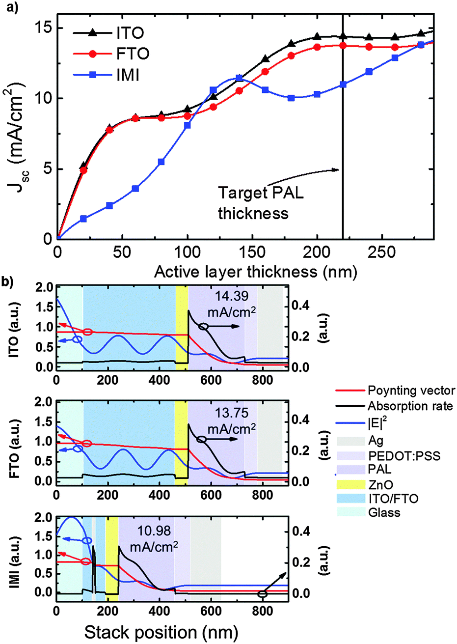 | ||
| Fig. 1 (a) Optical simulation of the resulting Jsc as a function of the active layer thickness for different electrode materials: ITO, FTO, IMI and (b) calculations on Poynting vector, absorption rate and intensity of the electric field (|E|2) as a function of the stack position. | ||
The simulations show a substantial agreement with the experimental results. The substitution of the ITO electrode with IMI causes, according to the TMF simulations (Fig. 1a) and in agreement with the experimental results, a significant loss in short circuit current (about 3.4 mA cm−2) and thus a predicted PCE loss of more than 24% compared to the reference device. In order to further investigate the reasons for the diminished Jsc in the IMI based device, we calculated the electric field intensity distribution in the stack15,16 at λ = 650 nm, which is the absorption maximum of the PAL (Fig. S1b, ESI†). Furthermore, we calculated the spatial distribution of the Poynting vector,15 depicting the energy flux in the stack and its spatial derivative, and the absorption rate. This quantifies the absorption in each layer composing the stack. In Fig. 1b the electric field intensity (|E|2), the Poynting vector and the absorption rate are shown as functions of the position in the stack for ITO, FTO and IMI based electrodes. The parasitic absorption of the silver layer in the IMI electrode reduces the photogenerated current in the PAL by around 0.9 mA cm−2 in the wavelength range 350–900 nm, according to the TMF calculations.
In an ideal up-scaling process, independently of the chosen substrate (flexible or rigid) and the processing technique (slot-die coating or doctor blading), it should be possible to obtain the above optically simulated efficiencies (Table 1) also for large area modules, provided the electrical interconnection of the cells does not lead to additional resistive losses and does not cause photoactive area losses. However, this is physically not possible, as shown in Fig. 2a: in fact the interconnection region (distance between P1 and P3, called patterning length ![[small script l]](https://www.rsc.org/images/entities/char_e146.gif) ) is not photoactive and furthermore may induce an additional resistance in the P2 line, where the top and bottom electrodes are in contact (interconnect resistance, Rint). High sheet resistances of top (Rs,top) and bottom (Rs,bottom) electrodes are as well causes of additional resistive losses when the cell length exceeds the dimensions of the single cells which are used as the references. The ratio between the active area length (L) and the sum of active area length and the patterning length (L + ) is usually referred to as geometric fill factor (GFF). According to finite element simulations,17 the previously mentioned losses can be minimized if (i) L is kept between 3 to 5 mm, (ii) Rint is well below 100 mΩ cm2, and (iii) is as small as technically possible. Satisfying these three conditions can be considered the main challenge to be faced: as previously shown,10 complying with these requirements allows the PCE loss from a single cell to a module to be as low as 4–6%. However, commonly reported patterning methods, such as one-dimensional slot-die coating, screen printing or spray coating10 do not allow us to achieve < 1 mm and reported modules6,18–20 show active cell lengths in the order of 0.8–1 cm, leading to prominent losses in the overall PCE of the modules compared to the single cells. Laser structuring by fs-lasers has already proven to be a successful candidate for monolithic integration of thin film solar cells with patterning lengths as small as 150 μm.21,22 In this work, we have managed to reduce this value to as little as 80 μm.
) is not photoactive and furthermore may induce an additional resistance in the P2 line, where the top and bottom electrodes are in contact (interconnect resistance, Rint). High sheet resistances of top (Rs,top) and bottom (Rs,bottom) electrodes are as well causes of additional resistive losses when the cell length exceeds the dimensions of the single cells which are used as the references. The ratio between the active area length (L) and the sum of active area length and the patterning length (L + ) is usually referred to as geometric fill factor (GFF). According to finite element simulations,17 the previously mentioned losses can be minimized if (i) L is kept between 3 to 5 mm, (ii) Rint is well below 100 mΩ cm2, and (iii) is as small as technically possible. Satisfying these three conditions can be considered the main challenge to be faced: as previously shown,10 complying with these requirements allows the PCE loss from a single cell to a module to be as low as 4–6%. However, commonly reported patterning methods, such as one-dimensional slot-die coating, screen printing or spray coating10 do not allow us to achieve < 1 mm and reported modules6,18–20 show active cell lengths in the order of 0.8–1 cm, leading to prominent losses in the overall PCE of the modules compared to the single cells. Laser structuring by fs-lasers has already proven to be a successful candidate for monolithic integration of thin film solar cells with patterning lengths as small as 150 μm.21,22 In this work, we have managed to reduce this value to as little as 80 μm.
 | ||
| Fig. 2 (a) Scheme of the cross section and (b) top view of monolithically interconnected cells in a module, with L active cell length and patterning length. The modules prepared in this work have dimensions L + = 5 mm, D = 50 mm and 14 cells in series. (c) Interconnection region of a flexible module on an IMI electrode with P1, P2 and P3 visible. The total width of the interconnection region is 80 μm. | ||
Following the prescriptions (i) to (iii), a suitable module layout was chosen (Fig. 2b) for the fabrication of modules, using the following parameters: L + = 5 mm, = 80 μm, P2 width = 20 μm. Subsequently, FEM simulations were performed to determine the potential of modules with this layout, inserting the experimental values of Jsc, FF, and Voc of the best performing single cells and Rs,top = 0.1 Ω sq−1 (evaporated silver) and Rs,bottom = 8 Ω sq−1 (IMI,12 FTO, ITO) for the sheet resistances of the materials employed for top and bottom electrodes, respectively, and using the literature value Rint = 11 mΩ cm223 for the interconnect resistance. Bus bar induced losses were not accounted for in this simulation. Fig. 3a provides a scheme of electrical resistances added in the simulation to the experimental JV curves of the single cells as reported in Table 2.
 | ||
| Fig. 3 (a) Electrical resistances of bottom (Rs,bottom) and top (Rs,top) electrodes and interconnect resistance (Rint) added to the experimental JV curves of single cells (cell1, cell2,…) in the FEM simulations. (b) Slot-die coating process and (c) dried film of the photoactive layer on a ZnO coated, pre-patterned substrate; (d) 35 cm2 active area glass module and (e) 35 cm2 flexible module. | ||
| J sc (mA cm−2) | V oc (V) | FF (%) | PCE (%) | ||||
|---|---|---|---|---|---|---|---|
| Cells (exp.) | Modules (FEM) | Cells (exp.) | Modules (FEM) | Cells (exp.) | Modules (FEM) | ||
| ITO | 13.45 | 13.44 | 0.77 | 64 | 59 | 6.6 | 6.2 |
| FTO | 11.42 | 11.42 | 0.81 | 66 | 61 | 6.1 | 5.6 |
| IMI | 11.50 | 11.46 | 0.77 | 62 | 58 | 4.9 | 4.5 |
The FEM simulations show that efficiencies of 6.2% for ITO based modules, 5.6% for FTO modules and 4.5% for IMI modules are achievable. The slightly lower fill factors in the module with respect to the single cells are mainly due to the additional series resistance introduced by the interconnection. According to the simulations, Jsc should not be affected at all.
Finally, modules were prepared according to the layout described above. Modules on glass/FTO substrates were coated by doctor-blading whereas PET/IMI modules were slot-die coated on a roll coater. A scheme illustrating the working principle of doctor-blading and slot-die coating is provided in Fig. S2 (ESI†) and the roll coating of the active layer is shown in Fig. 3b and c. A finished glass/FTO module and a PET/IMI module are provided in Fig. 3d and e. Experimental IV curves of FTO and IMI based modules are provided in Fig. 4.
 | ||
| Fig. 4 (a) Light and dark (b) experimental IV curves of the modules prepared in this work. | ||
The performances of the prepared modules are summarized in Table 3. Efficiencies as high as 5.3% are obtained for hero glass modules, corresponding to a negligible PCE loss of 3.5% compared to the reference hero device (see Table 2). Flexible hero modules on IMI achieve efficiencies higher than 4%, with a PCE loss of only 7% compared to the reference device, which is mainly due to a reduced Jsc. Interestingly, the average PCE values for FTO, doctor-bladed modules are significantly lower compared to the hero module due to the fluctuations in Jsc from module to module. The average values for the slot die coated modules on IMI, are instead consistent with the hero module, showing a variation in Jsc of only 2%. This shows that slot-die coating, with a continuous, precise ink supply while coating, is a suitable candidate for upscaling.
| Active area (mm2) | I/module active area (mA cm−2) and (Jsc (mA cm−2) of the single cells in the module) | V oc (V) | FF (%) | PCE (%) | PCE loss to ref. cell | |
|---|---|---|---|---|---|---|
| FTO best module | 3500 | 0.820 (11.48) | 10.50 | 62 | 5.28 | 3.5%* |
| Average on 6 modules (FTO) | 3500 | 0.775 (10.85) | 10.38 | 56 | 4.49 | 16%** |
| IMI best module | 3500 | 0.630 (8.82) | 10.70 | 62 | 4.18 | 7.0%* |
| Average on 6 modules (IMI) | 3500 | 0.619 (8.66) | 10.70 | 60 | 3.97 | 11%** |
| IMI Module | 9800 | 0.613 (8.58) | 10.70 | 60 | 3.95 | 12%* |
High quality, highly uniform coatings are necessary to have a uniform photogenerated current across the photoactive area. In order to verify the homogeneity of the printed active layer, we measured the optical density and calculated the dry film thickness of the slot die coated layer as shown in Fig. S3 (ESI†). The spatially resolved map obtained shows that variations in thickness in the order of ±20 nm can occur in the region of the printed layer corresponding to the active area of the module. According to TMF simulations this corresponds to the changes in the predicted Jsc of ±0.5–0.6 mA cm−2 (Fig. S2, ESI†), thus reducing the current delivered by the modules. Variations in the thickness of the electron injection layer and the hole injection layer can cause further oscillations of the Jsc and account for the losses of PCE as in Table 3.
The high quality of the slot die coatings is also confirmed by dark lock-in thermography (DLIT) measurements in the injection regime. A DLIT image of a slot-die coated 35 cm2 module is shown in Fig. S4 (ESI†). The slot-die coated module (PCE 3.95% as prepared) shows a high homogeneity of the locally dissipated power, indicating a homogeneous current and voltage distribution in the cells.24 From Fig. S3 (ESI†) and Table 3 it can be seen that the few hot spots do not affect the cells and performances of the module.25 Furthermore no interconnection issues between P1 and P3 could be detected.
Doctor-blading is instead affected by both batch-to-batch variations in the deposition procedure (for example, to the manual positioning of each substrate under the blade) as well as an intrinsic gradient of the thickness of the doctor-bladed layer.
4. Conclusions
In summary we have identified a successful way towards the minimization of the losses between hero cells, usually prepared on glass substrates with ITO electrodes, and roll to roll produced modules on PET/IMI. The optimization route starts necessarily from a quantitative evaluation of the optically induced losses in the upscaling process, mainly due to the choice of the electrodes and thicknesses of the electron-injection layers and hole-injection layers. The short circuit current of the devices can be reduced quite significantly upon replacing ITO by IMI electrodes, due to the lower transparency and interference effects of the latter, which in case of PBTZT-stat-BDTT-8:PCBM photoactive layer can be as high as 30% compared to a reference ITO based electrode (Table 1). FEM simulations then allow us to assess the impact of the electrical layout of modules consisting of monolithically connected solar cells. The use of high resolution, ultra-fast laser structuring allows achieving record geometric fill factors up to 98.5% and dead areas below 80 μm, with P2 line width in the range of 20 μm yielding to simulated PCE losses of less than 8% compared to the hero devices (Table 2). Furthermore, the use of high precision coating techniques, such as slot-die coating, allows for a very good control of the thickness of the coated layers yielding to small differences in performance between modules and reference cells. The combination of information from optical and electrical simulations allows a very precise estimation of the achievable efficiencies in experimental trials, allowing to maximize the PCE of the modules and obtain, to the best of our knowledge, the highest PCE (4.2%) reported in the literature for large area, roll coated, flexible OPV modules and an efficiency higher than 5.3% for large area coated rigid modules. The exclusive use of commercially available materials and the minimization of the efficiency drop between hero cells and large area modules finally open the way to a successful production of large volumes of highly efficient modules.Acknowledgements
The authors acknowledge the Solar Factory of the Future as part of the Energy Campus Nuremberg (EnCN), which is supported by the Bavarian State Government (FKZ 20-3043.5); F. M. and H. D. S. acknowledge the German federal ministry of education and research (BMBF, grant no. 03EK3501).Notes and references
- S. B. Darling and F. You, RSC Adv., 2013, 3, 17633 RSC.
- Y. Liu, J. Zhao, Z. Li, C. Mu, W. Ma, H. Hu, K. Jiang, H. Lin, H. Ade and H. Yan, Nat. Commun., 2014, 5, 1–8 Search PubMed.
- W. S. Yang, J. H. Noh, N. J. Jeon, Y. C. Kim, S. Ryu, J. Seo and S. Il Seok, Science, 2015, 348, 1234–1237 CrossRef CAS PubMed.
- R. Sondergaard, M. Hosel, D. Angmo, T. T. Larsen-Olsen and F. C. Krebs, Mater. Today, 2012, 15, 36–49 CrossRef CAS.
- D. Angmo and F. C. Krebs, J. Appl. Polym. Sci., 2013, 129, 1–14 CrossRef CAS.
- T. R. Andersen, H. F. Dam, M. Hösel, M. Helgesen, J. E. Carle, T. T. Larsen-Olsen, S. A. Gevorgyan, J. W. Andreasen, J. Adams, N. Li, F. Machui, G. D. Spyropoulos, T. Ameri, N. Lemaitre, M. Legros, A. Scheel, D. Gaiser, K. Kreul, S. Berny, O. R. Lozman, S. Nordman, M. Valimaki, M. Vilkman, R. R. Sondergaard, M. Jorgensen, C. J. Brabec and F. C. Krebs, Energy Environ. Sci., 2014, 7, 2925–2933 CAS.
- G. D. Spyropoulos, P. Kubis, N. Li, D. Baran, L. Lucera, M. Salvador, T. Ameri, M. M. Voigt, F. C. Krebs and C. J. Brabec, Energy Environ. Sci., 2014, 3284–3290 CAS.
- F. Machui, L. Lucera, G. D. Spyropoulos, J. Cordero, S. A. Ali, P. Kubis, T. Ameri, M. M. Voigt and C. J. Brabec, Sol. Energy Mater. Sol. Cells, 2014, 441–446 CrossRef CAS.
- M. A. Green, K. Emery, Y. Hishikawa, W. Warta and E. D. Dunlop, Prog. Photovoltaics, 2014, 22, 701–710 Search PubMed.
- L. Lucera, P. Kubis, F. W. Fecher, C. Bronnbauer, M. Turbiez, K. Forberich, T. Ameri, H.-J. Egelhaaf and C. J. Brabec, Energy Technol., 2015, 3, 373–384 CrossRef.
- S. Berny, N. Blouin, A. Distler, H.-J. Egelhaaf, M. Krompiac, A. Lohr, O. R. Lozman, G. E. Morse, L. Nanson, A. Pron, T. Sauermann, N. Seidler, S. Tierney, P. Tiwana, M. Wagner and H. Wilson, Adv. Sci., 2015 DOI:10.1002/advs.201500342.
- P. Kubis, L. Lucera, F. Machui, G. Spyropoulos, J. Cordero, A. Frey, J. Kaschta, M. M. Voigt, G. J. Matt, E. Zeira and C. J. Brabec, Org. Electron., 2014, 15, 2256–2263 CrossRef CAS.
- L. A. A. Pettersson, L. S. Roman and O. Inganäs, J. Appl. Phys., 1999, 86, 487 CrossRef CAS.
- T. Ameri, G. Dennler, C. Waldauf, P. Denk, K. Forberich, M. C. Scharber, C. J. Brabec and K. Hingerl, J. Appl. Phys., 2008, 103, 084506 CrossRef.
- N.-K. Persson and O. Inganäs, Sol. Energy Mater. Sol. Cells, 2006, 90, 3491–3507 CrossRef CAS.
- C.-C. Chen, W.-H. Chang, K. Yoshimura, K. Ohya, J. You, J. Gao, Z. Hong and Y. Yang, Adv. Mater., 2014, 5670–5677 CrossRef CAS PubMed.
- F. W. Fecher, A. Pérez Romero, C. J. Brabec and C. Buerhop-Lutz, Sol. Energy, 2014, 105, 494–504 CrossRef CAS.
- J. E. Carle, M. Helgesen, M. V. Madsen, E. Bundgaard and F. C. Krebs, J. Mater. Chem. C, 2014, 2, 1290–1297 RSC.
- F. C. Krebs, T. Tromholt and M. Jorgensen, Nanoscale, 2010, 2, 873–886 RSC.
- F. C. Krebs, Sol. Energy Mater. Sol. Cells, 2009, 93, 1636–1641 CrossRef CAS.
- P. Kubis, N. Li, T. Stubhan, F. Machui, G. J. Matt, M. M. Voigt and C. J. Brabec, Prog. Photovoltaics, 2013, 23, 238–246 Search PubMed.
- F. Guo, P. Kubis, T. Przybilla, E. Spiecker, A. Hollmann, S. Langner, K. Forberich and C. J. Brabec, Adv. Energy Mater., 2014, 1–9 Search PubMed.
- H. Hoppe, M. Seeland and B. Muhsin, Sol. Energy Mater. Sol. Cells, 2012, 97, 119–126 CrossRef CAS.
- J. Adams, M. Salvador, L. Lucera, S. Langner, G. D. Spyropoulos, F. W. Fecher, M. M. Voigt, S. A. Dowland, A. Osvet, H.-J. Egelhaaf and C. J. Brabec, Adv. Energy Mater., 2015, 1501065 Search PubMed.
- S. Besold, U. Hoyer, J. Bachmann, T. Swonke, P. Schilinsky, R. Steim and C. J. Brabec, Sol. Energy Mater. Sol. Cells, 2014, 124, 133–137 CrossRef CAS.
Footnote |
| † Electronic supplementary information (ESI) available. See DOI: 10.1039/c5ee03315b |
| This journal is © The Royal Society of Chemistry 2016 |