
Monolithic perovskite/silicon-heterojunction tandem solar cells processed at low temperature†
Steve
Albrecht‡
*a,
Michael
Saliba‡
*b,
Juan Pablo
Correa Baena‡
*c,
Felix
Lang
a,
Lukas
Kegelmann
a,
Mathias
Mews
a,
Ludmilla
Steier
d,
Antonio
Abate
d,
Jörg
Rappich
a,
Lars
Korte
a,
Rutger
Schlatmann
e,
Mohammad Khaja
Nazeeruddin
b,
Anders
Hagfeldt
c,
Michael
Grätzel
d and
Bernd
Rech
a
aHelmholtz-Zentrum Berlin für Materialien und Energie GmbH, Institut für Silizium-Photovoltaik, Kekuléstraße 5, 12489 Berlin, Germany. E-mail: steve.albrecht@helmholtz-berlin.de
bGroup for Molecular Engineering of Functional Materials, Institute of Chemical Sciences and Engineering, École Polytechnique Fédérale de Lausanne, 1951-Sion, Switzerland. E-mail: michael.saliba@epfl.ch
cLaboratory for Photomolecular Science, Station 6, Lausanne, CH 1015, Switzerland. E-mail: juan.correa@epfl.de
dLaboratory for Photonics Swiss Federal Institute of Technology (EPFL), Station 6, Lausanne, CH 1015, Switzerland
eHelmholtz-Zentrum Berlin für Materialien und Energie GmbH, PVcomB, Schwarzschildstr. 3, 12489 Berlin, Germany
First published on 27th October 2015
Abstract
Tandem solar cells combining silicon and perovskite absorbers have the potential to outperform state-of-the-art high efficiency silicon single junction devices. However, the practical fabrication of monolithic silicon/perovskite tandem solar cells is challenging as material properties and processing requirements such as temperature restrict the device design. Here, we fabricate an 18% efficient monolithic tandem cell formed by a silicon heterojunction bottom- and a perovskite top-cell enabling a very high open circuit voltage of 1.78 V. The monolithic integration was realized via low temperature processing of the semitransparent perovskite sub-cell where an energetically aligned electron selective contact was fabricated by atomic layer deposition of tin oxide. The hole selective, transparent top contact was formed by a stack of the organic hole transport material spiro-OMeTAD, molybdenum oxide and sputtered indium tin oxide. The tandem cell design is currently limited by the photocurrent generated in the silicon bottom cell that is reduced due to reflectance losses. Based on optical modelling and first experiments, we show that these losses can be significantly reduced by combining optical optimization of the device architecture including light trapping approaches.
Broader contextThe silicon photovoltaic industry is one of the most important sources of solar energy. Improving silicon solar cells, however, is becoming increasingly challenging as they start reaching their theoretical efficiency limit. Organic–inorganic perovskite materials, due to their complementary band gaps, have become attractive for tandem cell integration with crystalline silicon (c-Si), offering an inexpensive option to significantly boost state-of-the-art silicon single junctions. So far, the reported c-Si/perovskite tandems require high temperature processing (∼500 °C) incompatible with the currently best performing silicon technology: the silicon heterojunction (SHJ). In this work, we present a monolithic, 2-terminal c-Si/perovskite tandem solar cell with a planar perovskite top-cell and a SHJ bottom cell using a low temperature processed perovskite sub-cell. We achieve a tandem cell efficiency of 19.9% with a short circuit current of 14 mA cm−2, a voltage of 1.78 V, and a FF = 79.5% for the reverse scan direction with a stabilized power output of 18.1% which is one the highest reported values to date. Furthermore, we show that optical losses limiting the photocurrent in the silicon sub-cell can be reduced using a textured foil for anti-reflectance and light trapping. Thus, further improvements of the presented silicon/perovskite tandem are attainable. Already, the high open circuit voltage has direct consequences for low-cost water splitting and CO2 reduction. |
Solar cells made from organic–inorganic perovskites such as CH3NH3PbI3 have shown tremendous power conversion efficiency (PCE) enhancements from 3.8 to over 20% in the last six years.1,2 This is unprecedented as none of the other solar cell technologies has shown such spectacular improvements in a comparable time frame.3,4
Organic–inorganic perovskite materials are promising solar cell absorbers as they show unique optoelectronic properties and can be processed from solution enabling low lost, high throughput fabrication at low temperatures on flexible substrates.5,6 The optical band-gap of CH3NH3PbI3 is 1.57 eV and can be tuned via halide replacement7 or cation exchange.8 The perovskite material has a high absorption coefficient across the entire visible range together with a sharp onset and very low sub band-gap absorption.9 Thus, a perovskite layer thickness of around 500 nm is sufficient to absorb a very high portion of the incident light,4 and even thinner absorber layers can be used if light recycling schemes are employed.10,11 Due to the negligible exciton binding energy at room temperature,12 the long carrier diffusion length,13,14 the bipolar charge transport with high charge carrier mobilities,15,16 and the strongly reduced recombination in the bulk15,17 and at the surface,18 free charge carriers are formed directly upon photoexcitation. These are, in turn, effectively collected at the selective contacts, enabling internal quantum efficiencies close to 100%,19 a high fill factor (FF), and open circuit voltage (Voc) resulting in a record efficiency over 20%.4
These unique properties make organic–inorganic perovskites attractive for tandem cell integration in combination with crystalline silicon (c-Si). In the c-Si/perovskite tandem cell, higher energy photons are absorbed within the perovskite sub-cell and converted at a high voltage without significant losses from thermalization. Infrared photons are transmitted through the perovskite and lead to photogeneration in the c-Si sub-cell, covering a wide spectral range up to 1.12 eV defined by the band-gap of c-Si. This tandem design has a detailed balance limit of ca. 40%,20 thus, overcoming the Shockley–Queisser limit of silicon single junctions being around 33%.21
Recently, experimental attempts have been made to combine c-Si and perovskite sub-cells into 4-terminal mechanically stacked tandem cells which requires a perovskite sub-cell with two transparent electrodes where one transparent electrode is processed directly on top of the perovskite or the charge selective layer, typically spiro-OMeTAD. Lang et al. recently developed a method for fabricating transparent electrodes by using a water-free transferred graphene layer achieving a 4-terminal device with 13.2%.22 Bailie and coworkers used transferred layers of silver nanowires and reached an efficiency of 17.0% in a 4-terminal device.23 Löper et al. used sputtered ITO on top of the spiro-OMeTAD that is protected by a 30 nm thick MoO3 layer resulting in device efficiencies of 13.7%.24 This PCE was increased to 18.2% by Werner et al. using zinc doped indium oxide (IZO) contacts sputtered without reactive oxygen gas, thus enabling direct fabrication on a spiro-OMeTAD layer25 without losses from sputter damage or increased series resistance due to thick MoO3 interlayers. With a soft sputter process of aluminum doped zinc oxide (AZO), Kranz et al. achieved to reduce the sputter damage at thin MoO3 interlayers fabricating a copper indium gallium selenide (CIGS)/perovskite stack resulting in a 19% efficient 4-terminal device.26
The monolithic (2-terminal) integration of perovskite and c-Si was realized recently by Mailoa, Bailie and coworkers,27 using a diffused silicon homojunction cell with an intermediate tunnel recombination contact: highly n-doped amorphous hydrogenated silicon, (n++)a-Si:H, was deposited on the diffused p++ emitter and then partially crystallized in a high temperature step. Silver nanowires were implemented as top contact, similar to the 4-terminal device, in a previous publication by Bailie et al.23 This resulted in a stabilized efficiency of 13.7% with a Voc of 1.56 V. This efficiency is lower than their reported 4-terminal device, which is partially caused by the parasitic light absorption of the doped spiro-OMeTAD layer.27 The parasitic absorption complicates the realization of current matching, being a prerequisite to achieve high efficiencies in monolithic tandem cells.
All of the reported c-Si/perovskite tandem designs use compact and/or mesoporous TiO2 that is typically sintered at high temperatures of 500 °C. Devices employing this mesoporous TiO2 scaffold yielded the highest efficiencies to date4 with least pronounced hysteretic behavior as compared to planar devices without the use of mesoporous TiO2.2 Unfortunately such high temperatures are not suitable for the best performing silicon technology to date, i.e. the a-Si:H/c-Si silicon heterojunction (SHJ) with 25.6% efficiency.28 Owing to the high surface passivation quality induced by (i)a-Si:H, SHJ solar cells can have high open circuit voltages up to 750 mV,29 which is significantly higher as compared to diffused homojunction cells showing a maximum Voc around 700 mV. However, a major limitation is the thermal stability of a-Si:H: the hydrogen, passivating the amorphous network becomes mobile at ∼200 °C and eventually effuses, reducing the passivation quality of the a-Si:H/c-Si interface and thus the device performance. Therefore, in the monolithic integration of perovskite and SHJ solar cells, high temperature sintering of the mesoporous or compact TiO2 layer is not feasible. One option to solve this problem would be a planar, i.e. mesoporous-free perovskite sub-cell with an electron-selective contact processed at low temperatures. However, there are very few reports showing planar, low-temperature devices with a stabilized high efficiency output.30,31 Recently, we have developed a new approach for manufacturing planar perovskite solar cells at temperatures below 120 °C by using atomic layer deposited (ALD) SnO2 as electron selective contact.32 We achieve almost hysteresis-free solar cells with PCEs over 18% being fully compatible with silicon heterojunctions.32
Hence, in Fig. 1a, we present a monolithic, 2-terminal silicon/perovskite tandem solar cell with a planar perovskite top-cell and a (p,i)a-Si:H/(n)c-Si heterojunction bottom cell. The development results in a tandem cell efficiency of 19.9% with a short circuit current (Jsc) of 14.0 mA cm−2, Voc = 1.785 V, and FF = 79.5% for the reverse (=open circuit to short circuit) scan direction with a scan rate of 500 mV s−1. Due to hysteresis effects, the Voc and FF are reduced to 1.759 V and 77.3%, respectively when scanning in forward (=short circuit to open circuit) direction. This yields an efficiency of 19.1% in forward scan direction and 18.1% for the stabilized measurement. The latter is deduced from the stabilized current at maximum power point (MPP) in which the device is held at the MPP voltage and the current is tracked over time (under AM 1.5G illumination), thus providing a PCE under operational conditions.33 To the best of our knowledge, this is the highest reported efficiency for a monolithic perovskite/c-Si tandem cell to date. We show that the tandem cell efficiency is limited by the current in the silicon sub-cell, and we present a strategy to improve the photocurrent by implementing effective light management and light trapping strategies.
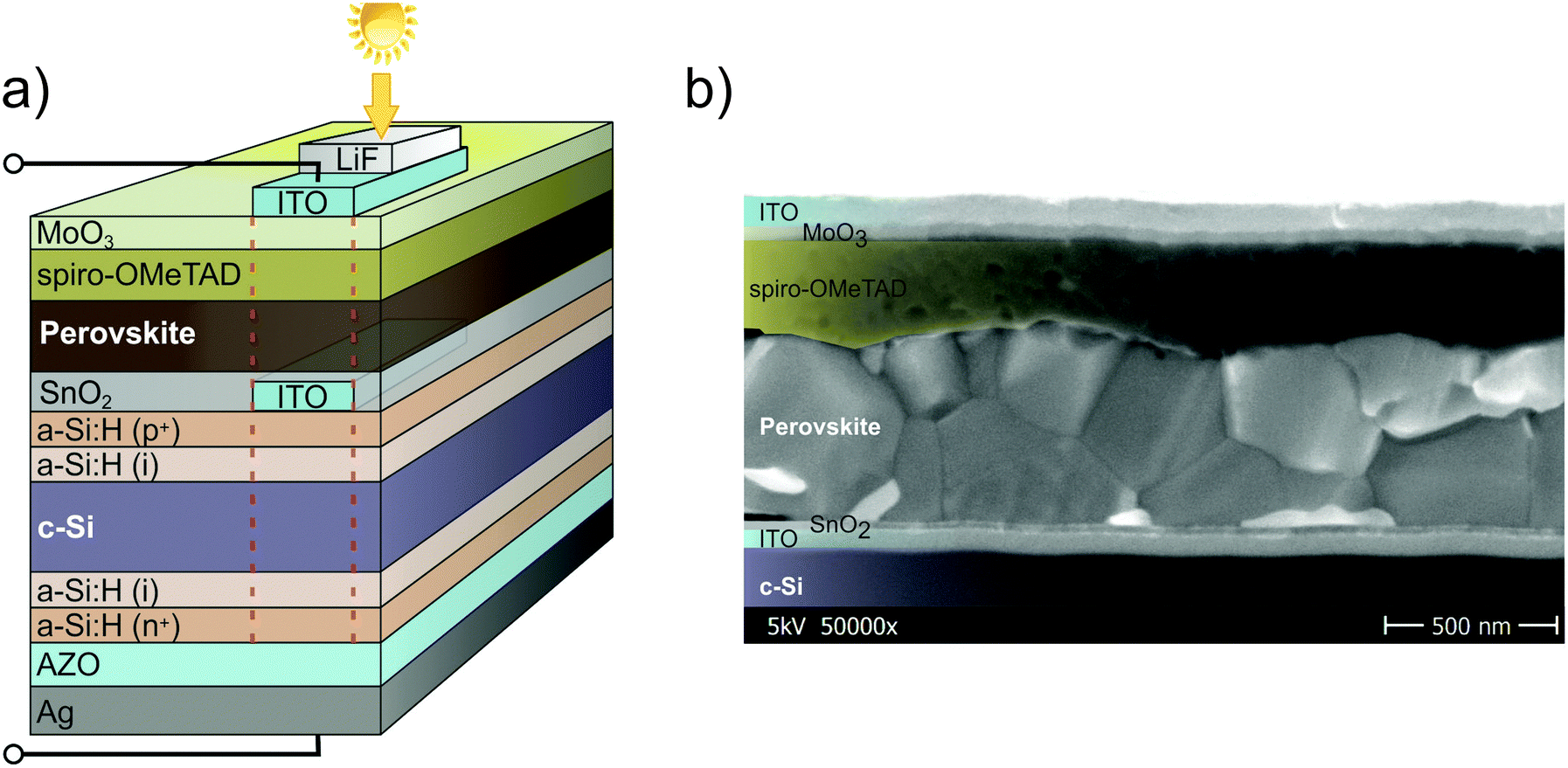 | ||
| Fig. 1 (a) Schematic device design of the silicon heterojunction/perovskite tandem solar cell. The red dashed line indicates the active area. (b) Cross sectional scanning electron micrograph of a typical monolithic tandem solar cell. | ||
Fig. 1a displays the device design of the monolithic tandem solar cell developed in this study. A both-side polished 250 μm thick n-type silicon wafer was used to fabricate the silicon bottom cell. Thin layers of intrinsic and doped a-Si:H were deposited via plasma enhanced chemical vapor deposition (PECVD), in order to form a p/n junction and back surface field (BSF) on the front and rear of the wafer, respectively. After that, ITO is deposited on the front side by means of sputtering through shadow masks. The back side is fully covered with aluminum doped zinc oxide (AZO) and silver, both deposited by sputtering. On the front side, SnO2 is deposited via ALD forming, together with the ITO, a recombination contact between both sub-cells. The perovskite is deposited from spin coating a liquid precursor followed by another spin coated layer of doped spiro-OMeTAD. Then a MoO3 layer was deposited via thermal evaporation and finally the top ITO contact was sputtered through the same shadow mask as used for the first ITO layer connecting both sub-cells. Both ITO layers are aligned exactly on top of each other. To reduce the reflection at the air/front ITO interface, LiF was thermally evaporated on the finished cell. The active area is defined by the aligned ITO areas, as indicated by the red dashed lines in Fig. 1a. Furthermore, a shadow mask is used during the measurements of the illuminated JV characteristics.
Fig. 1b displays a scanning electron micrograph (SEM) cross section image of the tandem cell structure. The individual layers can be clearly identified. In the very bottom of the image, the silicon wafer is found. On top of that, the recombination contact formed by ITO and SnO2 is seen. The perovskite crystals show vertical sizes of several hundred nanometers. Some crystals can be found that are as high as the total film thickness (left side of the image). The spiro-OMeTAD layer covers the perovskite film uniformly and the transparent top contact formed by MoO3 and ITO completes the device.
In the monolithic tandem device, light travels through the top contact and the spiro-OMeTAD layer before being absorbed in the perovskite layer. This is the direction indicated by the black arrow in Fig. 2a, and is different from typical perovskite single-junction geometries (light path indicated by the grey arrow).34 Doped spiro-OMeTAD has broad absorption peaks at 380 and 500 nm,35–37 causing observable parasitic absorption,27 that reduces the photocurrent as seen in Fig. 2a where we compare the external quantum efficiency (EQE) spectra for a semitransparent perovskite single-junction with different illumination directions. Below 400 nm almost no light can pass through the spiro-OMeTAD layer and above 400 nm, the EQE is reduced by 5–10% which results in an overall reduction of the generated photocurrent under AM 1.5G illumination of 2.2 mA cm−2. However, despite the parasitic absorption in the spiro-OMeTAD layer when illuminating from the top side, the EQE still plateaus at about 70% between 400 and 750 nm, allowing to generate at least 15 mA cm−2 in the perovskite sub-cell. Note that in the monolithic tandem stack, the light distribution will vary from that in the semitransparent single cell. Due to the high refractive index of the silicon (n ∼ 4), part of the light can be reflected back into the perovskite sub-cell. Thus even more than 15 mA cm−2 can be generated in the perovskite sub-cell of the tandem device with the spiro-OMeTAD layers used in this work.
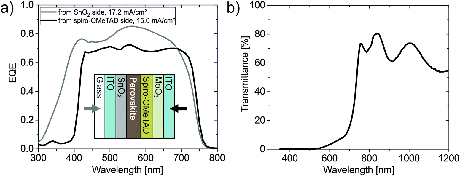 | ||
| Fig. 2 (a) External quantum efficiency (EQE) of the semitransparent perovskite single junction for two illumination directions as indicated in the inset. The grey line corresponds to illumination from the glass substrate side as indicated by the grey arrow, the black line corresponds to illumination through the top contact as indicated by the black arrow. (b) Total transmittance of the semitransparent perovskite single-junction. | ||
In addition, the perovskite has to transmit a high fraction of near infrared (NIR) light to generate a high photocurrent in the silicon sub-cell. Fig. 2b displays the total transmittance of the semitransparent perovskite single junction. The layer stack in this cell is almost identical to the sub-cell used in the tandem configuration with the only difference being the bottom ITO thickness and the glass substrate. No light is transmitted below wavelengths of 550 nm and the transmittance increases gradually in the range between 550 and 700 nm. In this range, the transmittance can be easily tuned by the perovskite thickness. The transparent contact enables an average transmittance of 70% in the wavelength range between 750 and 1100 nm, which is comparable to the semitransparent perovskite single-junctions reported by Kranz et al.26
Thus, with the high transmittance in the NIR regime, our device design is suitable for a monolithic tandem because the silicon bottom-cell can absorb the NIR light. Fig. 3a shows the JV characteristics measured for the monolithic tandem cell and the reference single-junctions, i.e. the silicon heterojunction and the perovskite cell in standard configuration with opaque gold electrodes. The corresponding performance data can be found in Table 1. The silicon heterojunction reference with 1 cm2 active cell area is comparable to that used in the tandem configuration except that a metal grid on top of the ITO is applied to effectively collect the current from the complete active area. Clearly, the full potential of the SHJ concept is not realized in the tandem cell. This is mainly because spin-coating of the perovskite sub-cell requires to utilize a planar Si wafer. The planar wafer surface leads, on the one hand, to a several mA cm−2 lower Jsc as compared to standard SHJ cells,38 since the light trapping induced by a random pyramid texture on the wafer in such cells is absent here. On the other hand, we found that also Voc and FF are reduced as compared to our textured reference cells. This is most likely due to different PECVD growth conditions of the a-Si:H on flat wafers, leading to a decreased a-Si:H/c-Si interface passivation and reduced conductivity/increased contact resistance, as the a-Si:H and TCO deposition conditions are currently optimized for textured cells. An optimization of the PECVD and sputter process on flat wafers is planned in future experiments, especially in order to improve the FF.
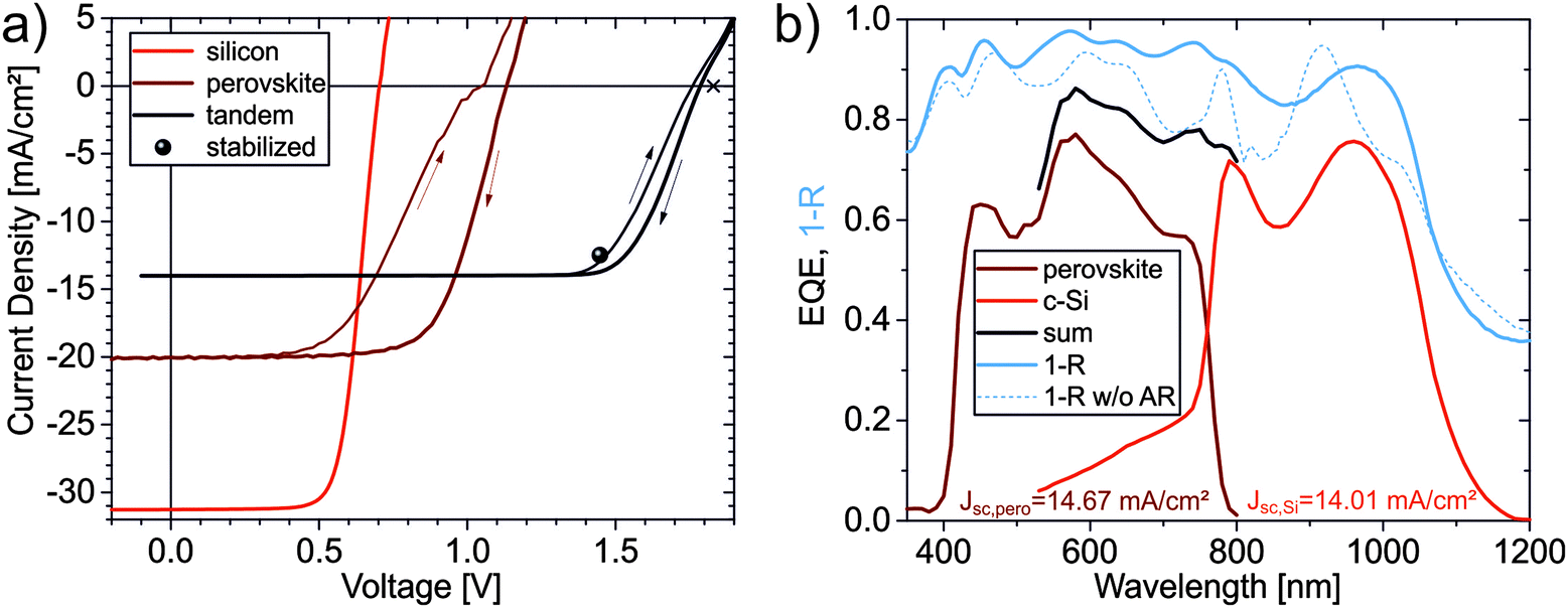 | ||
| Fig. 3 (a) JV characteristics measured at a scan rate of 500 mV s−1. The red line is the silicon single junction cell and the brown line corresponds to the perovskite reference single junction cell with non-transparent Au contacts in forward and reverse scan (as indicated by the arrows). The black curve is the monolithic tandem cell with additional LiF anti-reflectance (AR) coating in forward and reverse scan direction. The black cross indicates the sum of the Voc of the reference single-junctions (b) external quantum efficiency of the individual sub-cell in the monolithic tandem device with AR coating. Also shown are the sum of the individual EQE spectra, the currents from multiplication of the EQE with the AM 1.5G spectrum and integration over the measured wavelength range, and 1-reflectance of the complete monolithic stack with and without AR coating. | ||
| Device | J sc (EQE) [mA cm−2] | J sc [mA cm−2] | V oc [mV] | FF [%] | PCE [%] |
|---|---|---|---|---|---|
| a From integration of the EQE of the respective sub-cell measured with background bias light, 1st value: perovskite, 2nd value: silicon. b Measured with an aperture mask under simulated AM 1.5G illumination calibrated to 100 mW cm−2. c The measured Jsc is adjusted to match the value of the limiting sub-cell as determined from the EQE spectra (see text). d The stabilized efficiency is deduced from the average value of the current transient measurements (see ESI) at MPP = 1.45 V. e Single reference junctions in standard device configuration. f 1 cm2 active area with metal grid. g 0.27 cm2 active area with non-transparent Au contacts. | |||||
| Tandem cell | 14.67/14.01 | ||||
| Reverse scanb | 11.8 | 1785 | 79.5 | 16.8 | |
| Forward scanb | 11.8 | 1759 | 77.3 | 16.1 | |
| Reverse scanc | 14.0 | 1785 | 79.5 | 19.9 | |
| Forward scanc | 14.0 | 1759 | 77.3 | 19.1 | |
| Stabilized efficiencyd | 18.1 | ||||
| Single junctionse | |||||
| Silicon (1 cm2)f | 31.3 | 703 | 71.4 | 15.7 | |
| Perovskite reverseg | 20.1 | 1130 | 68.3 | 15.5 | |
| Perovskite forwardg | 20.1 | 1048 | 49.3 | 10.4 | |
The perovskite single junction fabricated on glass/ITO substrates achieved a Voc of 1.13 V, comparable to the high values we have reported when utilizing a SnO2 electron selective contact that is energetically well aligned with the conduction band of the perovskite.32 Together with a FF of 68.3% and a short circuit current of 20.1 mA cm−2 this results in an efficiency of 15.5%. The high Voc of the perovskite single junction is beneficial for the tandem device. However, a more pronounced hysteresis is measured for the perovskite cell on ITO as compared to FTO electrodes.32 The hysteresis at a scan rate of 500 mV s−1 reduces the Voc and especially the FF when scanning the JV characteristics in forward (short circuit to open circuit) sweep direction. This finding was recently attributed to ion migration.39–43 Due to the hysteresis, the Voc and the FF are reduced to 1.05 V and 49.3%, respectively when scanning in forward direction. This results in an efficiency of the perovskite single junction of 10.4% in forward scan direction. In Fig. S2 (ESI†), we determine the stabilized current at maximum power point to be at 11.9% for the perovskite single junction. Interestingly, the influence of the hysteresis in the perovskite sub-cell on the tandem cell characteristics is less pronounced. This finding could potentially be caused by different morphological features on the silicon versus ITO/glass substrate which may affect the ionic movement dynamics. Furthermore, assuming that the hysteresis is originated by ion migration that is field driven, an altered electrical field distribution within the perovskite sub-cell in the monolithic tandem under operation could possibly change the hysteresis behaviour.43 The tandem cell exhibits a Voc of 1.785 V which is slightly below the sum of the Voc of both sub-cells in its single junction reference configuration (1.83 V, indicated by the cross in Fig. 3a). Note that in the silicon heterojunctions with small active area (0.16 cm2) as used in the tandem device, the Voc is decreased by 20 mV as compared to the 1 cm2 reference cells. Additionally, the Voc reduces by 30 mV for perovskite reference cells after deposition of the transparent contact layer (see ESI†). Thus, the measured Voc of the tandem cell is close to the potential value as defined by the respective single junction architectures. Interestingly, the tandem cell FF of 79.5% is significantly higher than that of both reference single junctions. Using the current calculated from the EQE spectra of the limiting sub-cell (silicon), the efficiency of the tandem in backward scan is 19.9% and the stabilized efficiency using the current measured at MPP over time yields 18.1%. The tandem device is remarkably stable as almost no difference in the JV characteristics can be found after storing the unencapsulated tandem devices in inert atmosphere for three months (see ESI†). Note that the current measured under the sun simulator calibrated to 100 mW cm−2 is slightly smaller as compared to the integrated EQE spectra (see Table 1). This is caused by the shadowing from the soft contact fingers reducing the current that can be generated in the tandem cell when measuring the JV curve, i.e. the current of the limiting sub-cell. In EQE measurements, the monochromated beam size is smaller as compared to the aperture area and thus no shadowing from the contact fingers occurs. Therefore, it is correct to estimate the efficiency using the current calculated from the EQE spectrum of the limiting sub-cell to be the Jsc of the tandem.
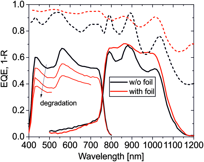 | ||
| Fig. 4 EQE and reflectance of a tandem device with and without the use of a textured anti-reflectance foil that is coupled via an index matching liquid to the front ITO surface. | ||
Fig. 3b displays the EQE spectra of the monolithic tandem cell, recorded with bias light to selectively address the sub-cells. To measure the perovskite in this 2-terminal device, a non-filtered halogen bias light was used. The silicon sub-cell was biased using monochromatic illumination at 450 nm using LED light. The overall EQE is 60–78% and interference fringes, especially in the silicon sub-cell can be detected. Also indicated are the integrated currents calculated from the EQE spectra assuming AM 1.5G illumination. Comparing the currents generated from the sub-cells, it follows that the silicon sub-cell is the current limiting one. Both sub-cells together generate 28.7 mA cm−2 which is lower than the Jsc of the silicon single junction reference cell with 31 mA cm−2. Thus optical losses limit the tandem cell due to the flat interfaces in the present cell design. The reflection shown in Fig. 3b is rather high with ca. 10% reflection throughout the perovskite absorption range and up to 25% in the NIR regime, especially when no anti-reflectance (AR) layer is used. The transparent and low refractive index material lithium fluoride (LiF) perfectly reduces the reflection losses at the air/ITO interface enabling a ca. 1.5 mA cm−2 higher photocurrent in the silicon sub-cell (see ESI†). With the AR coating, the sub-cells are almost current matched with currents of 14.7 and 14.0 mA cm−2 for the perovskite and silicon sub-cell under AM 1.5G illumination, respectively.
A strategy to further reduce the 10–15% reflection (present even with AR coating) is to apply effective light management. By optical simulations of the tandem stack, the optimum layer thicknesses can be calculated that reduces parasitic absorption and reflection even further. In our tandems, an ITO/SnO2 junction is used as recombination layer for the electrical contact between the sub-cells. However, ITO acts as intermediate reflector significantly reducing the light that is passed to the silicon bottom cell. Reducing this layer thickness or alternatively using a tunnel recombination junction formed by higher refractive index materials such as μc-Si:H would increase the current generated in the silicon heterojunction (see ESI†) and with that the tandem cell efficiency.
Recently, it was shown that thin film silicon cells with a textured foil on top of the glass substrate exhibit AR and light trapping properties enhancing the photocurrent especially in the long wavelength regime.44 Improving the photocurrent in the limiting silicon sub-cell would directly enhance the tandem cell efficiency. Fig. 4 shows the EQE and reflection of a perovskite/SHJ tandem cell with and without application of the same type as used by Ulbrich et al.,44 which is coupled with an index matching fluid to the front ITO surface. With the textured foil, we observe that the reflection is strongly reduced in the range of high reflectance around 600, 850 and 950 nm. Thus, also the EQE of the silicon sub-cell is mostly enhanced around 850 and 950 nm, improving the photocurrent by 1.2 mA cm−2. The reduced reflectance should also impact the perovskite sub-cell absorption, enhancing the EQE. Unfortunately, the perovskite sub-cell was degraded by the index matching liquid used in these experiments (Norland IML 150, or pure isopropanol), as indicated by the decreased EQE when repeating the measurement.
Further optical simulations indicate that a high photocurrent of 16.9 mA cm−2 can be generated in the silicon sub-cell together with 17.4 mA cm−2 in the perovskite cell when all the layer thicknesses in the stack are optimized, with a μc-Si:H/a-Si:H recombination layer, a reduced perovskite thickness, and an adjusted spiro-OMeTAD layer that optimizes the internal light distribution. This photocurrent can be generated under the assumption that all photons absorbed in the individual sub-cell at the respective wavelength range generate charges that can be collected at short circuit conditions.19,45 Thus, a Jsc of 16.9 mA cm−2 can be generated in the tandem cell when optimizing the layer stack even without any light trapping. Further assuming a FF of 80% which is reasonable when controlling the recombination layer and the MoO3 thickness and finally assuming a Voc of 1.85 V in the tandem cell, i.e. the sum of the open circuit voltages of the single junction reference devices, an efficiency of 25% is achievable with this device design.
In conclusion, we reported a monolithic silicon heterojunction/perovskite tandem solar cell with a high open circuit voltage between 1.76 and 1.78 V and a stabilized power output efficiency of 18.1% as deduced from stabilized current measurements at the maximum power point. The tandem cell shows an improved efficiency as compared to the reference single junction devices. The monolithic integration was realized via low temperature processing of the semitransparent perovskite sub-cell using atomic layer deposited SnO2 at low temperatures which functions as energetically aligned electron selective contact. A sandwich consisting of spin-coated spiro-OMeTAD, thermally evaporated MoO3, and sputtered ITO serves as the hole selective transparent top contact. To the best of our knowledge, the performance presented in this work is the highest efficiency reported for this type of tandem cell so far. This result can be further improved as the presented device design is limited by the insufficient absorption in the silicon bottom cell as the overall reflectance loss of the flat interfaces is not negligible. Furthermore, we showed a proof-of-concept for efficient anti-reflectance and light trapping using a textured foil to reduce optical losses. Optical device modelling suggests that the efficiency can be further increased when optimizing the layer stack thickness and the optics of the recombination contact. Utilizing these optimizations, the device design with flat interfaces has the potential to achieve 25% efficiency. Applying light trapping schemes to further enhance the matched Jsc and adjusting the perovskite band-gap to obtain a higher Voc, efficiencies around 30% are within reach. Therefore, this study highlights the great potential of monolithic silicon heterojunction/perovskite tandem solar cells.
Experimental
Solar cell fabrication
The experimental details on the silicon cell fabrication can be found elsewhere.38 Briefly, both-side polished float zone n-type (111) oriented wafers with 4 inch diameter, 255 μm thickness, and a resistivity of 2–5 Ω cm were used. The wafers were cleaned using the standard RCA process and the resulting oxides were removed by dipping in diluted hydrofluoric acid immediately before a-Si:H deposition.Intrinsic a-Si:H layers were deposited by standard PECVD processes using silane, SiH4, as precursor gas. The n-type and p-type doped a-Si:H layers were prepared by adding PH3 or B2H6 to the precursor gas, respectively.
On the front side of the wafer, 80 nm ITO was deposited by RF magnetron sputter deposition in a Roth & Rau sputter tool at a sputtering power of P = 70 W from a 2 inch ceramic target at room temperature.
The back contact was formed by sputtering 70 nm of aluminum doped zinc oxide (AZO) and 200 nm silver in a Leybold Optics A600V7 tool. After finishing the back contact, the silicon samples were annealed at 200 °C for 5 min in air.
15 nm-SnO2 layers were deposited at 118 °C using tetrakis(dimethylamino)tin(IV) (TDMASn, 99.99%-Sn, Strem Chemicals INC) and ozone at a constant growth rate of 0.065 nm per cycle measured by ellipsometry. TDMASn was held at 65 °C. Ozone was produced by an ozone generator (AC-2025, IN USA Incorporated) fed with oxygen gas (99.9995% pure, Carbagas) producing a concentration of 13% ozone in O2. Nitrogen was used as a carrier gas (99.9999% pure, Carbagas) with a flow rate of 10 sccm.
The perovskite precursor solution contained FAI (1 M), PbI2 (1.1 M), MABr (0.2 M) and PbBr2 (0.2 M) dissolved in anhydrous DMF![[thin space (1/6-em)]](https://www.rsc.org/images/entities/char_2009.gif) :DMSO 4:1 (v/v). The perovskite solution was spin coated in a two-step program at 1000 and 6000 rpm for 10 and 30 s, respectively. During the second step, 200 μL of chlorobenzene was poured on the spinning substrate 15 s prior to the end of the program. The substrates were then annealed at 100 °C for 1 h in a nitrogen filled glove box.
:DMSO 4:1 (v/v). The perovskite solution was spin coated in a two-step program at 1000 and 6000 rpm for 10 and 30 s, respectively. During the second step, 200 μL of chlorobenzene was poured on the spinning substrate 15 s prior to the end of the program. The substrates were then annealed at 100 °C for 1 h in a nitrogen filled glove box.
After the perovskite annealing, the substrates were cooled down for a few minutes and a spirofluorene linked methoxy triphenylamines (spiro-OMeTAD, Merck) solution (70 mM in chlorobenzene) was spin coated at 4000 rpm for 20 s. Spiro-OMeTAD was doped with bis(trifluoromethylsulfonyl)imide lithium salt (Li-TFSI, Sigma-Aldrich), tris(2-(1H-pyrazol-1-yl)-4-tert-butylpyridine)-cobalt(III) tris(bis(trifluoromethylsulfonyl)imide) (FK209, Dynamo) and 4-tert-butylpyridine (TBP, Sigma-Aldrich). The molar ratio of additives for spiro-OMeTAD was: 0.5, 0.03 and 3.3 for Li-TFSI, FK209 and TBP, respectively.
The 27 nm thick MoO3 was thermally evaporated in a MBraun vacuum chamber attached to a nitrogen filled glove-box at a base pressure around 7 × 10⁻⁷ mbar and deposition rates of 0.06 nm s−1.
Finally, the top contact was formed by 80 nm ITO deposited by DC magnetron sputter deposition in a Roth & Rau sputter tool at a sputtering power of P = 70 W from a 2 inch ceramic target at room temperature without further annealing of the sample.
Measurements
JV measurements were conducted using a “Steuernagel Lichtechnik” sun simulator, mimicking AM 1.5G spectra and adjusted to 100 mW cm−2 by measuring the short circuit current of a calibrated silicon solar cell (Fraunhofer ISE). The silicon reference and the monolithic tandem samples were temperature controlled to 25 °C during measurement. The silicon heterojunction reference cell has an active area of 1 cm2 defined by the top ITO layer, and an 8 × 8 mm aperture was used to define the active area during measurement. The perovskite reference cell has an active area of approximately 0.27 cm2 and an aperture of 4 × 4 mm2 was used to define the illuminated area during measurement. The monolithic tandem cell has an active area of 4 × 4 mm2 defined by both ITO layers and a 4 × 4 mm2 or 3.5 × 3.5 mm2 aperture was used during JV measurement.The current from integration of the EQE spectra was crosschecked under standard test conditions at the facilities of the Competence Centre Thin-Film- and Nanotechnology for Photovoltaics Berlin (PVcomB) using a Wacom dual light source (xenon and halogen lamp) Super Sun Simulator with AAA characteristics using smaller and sharp contact needles. Unfortunately, the sharp contact needles induce shunting losses when pressing on the top ITO and with that the FF and Voc are reduced. However, an identical Jsc is obtained, validating previously shown JV measurements.
The EQE was measured with monochromated light from a dual source lamp (tungsten or halogen) mechanically chopped to 78 Hz for the detection with a lock-in amplifier. The intensity of the lamp is checked with calibrated reference diodes. Constant background illumination was provided by 450 nm LED light or a halogen lamp. One sub-cell was optically biased with the background light having the suitable wavelength, the other sub-cell, not absorbing the bias light strongly, was measured with the chopped monochromatic light.
Transmission and reflection were measured with a PerkinElmer UV-VIS spectrometer, equipped with an integrating Ulbricht sphere and calibrated from a Fraunhofer ISE certified white standard.
For recording the cross section scanning electron micrograph (SEM), typical tandem devices were broken and the cross section was recorded with a Hitachi S-4100 at 50k magnification and 5 kV acceleration voltage.
Optical simulations
The optical simulations of the tandem stack were conducted using a transfer matrix algorithm implemented in the software “optical”.46 The optically thick c-Si layer was treated to be non-coherent in the simulation as the coherence length is much smaller than the layer thickness of 250 μm. As input to the simulations, optical data (n, k) of the layers were either extracted from spectral ellipsometry measurements or taken from literature for spiro-OMeTAD,47 and perovskite.48Author contributions
S. A., M. S., J. P. C. B., L. Ko., and B. R. developed the device concept and coordinated the project. S. A., M. S., J. P. C. B., F. L., L. Ke., M. W., L. S., and A. A prepared the devices. Measurements were performed by S. A., M. S., J. P. C. B., and F. L. The supervision of their team members involved in the project was realized by J. R., L. Ko., R. S., M. K. N., A. H., M. G., and B. R. The overall project was supervised by M. G. and B. R. All authors contributed to the analysis of the data and the writing of the paper.Acknowledgements
The authors would like to thank Thomas Lußky, Erhard Conrad, Kerstin Jacob, Mona Wittig, Carola Klimm, Tobias Hänel, and Karolina Mack from HZB as well as Manuel Hartig from TU Berlin for technical assistance. Financial support was provided by the European Union Seventh Framework Programme (FP7) through the MESO project (grant no. 604032). AA has received funding from the European Union's Seventh Framework Programme for research, technological development and demonstration under grant agreement no. 291771. We thank DSM Advanced Surfaces for providing the textured light trapping antireflection foil.References
- H. Zhou, Q. Chen, G. Li, S. Luo, T.-b. Song, H.-S. Duan, Z. Hong, J. You, Y. Liu and Y. Yang, Science, 2014, 345, 542 CrossRef CAS PubMed.
- N. J. Jeon, J. H. Noh, Y. C. Kim, W. S. Yang, S. Ryu and S. I. Seok, Nat. Mater., 2014, 13, 897 CrossRef CAS PubMed.
- A. Kojima, K. Teshima, Y. Shirai and T. Miyasaka, J. Am. Chem. Soc., 2009, 131, 6050 CrossRef CAS PubMed.
- W. S. Yang, J. H. Noh, N. J. Jeon, Y. C. Kim, S. Ryu, J. Seo and S. I. Seok, Science, 2015, 348, 1234 CrossRef CAS PubMed.
- M. Kaltenbrunner, G. Adam, E. D. Glowacki, M. Drack, R. Schwodiauer, L. Leonat, D. H. Apaydin, H. Groiss, M. C. Scharber, M. S. White, N. S. Sariciftci and S. Bauer, Nat. Mater., 2015, 14, 1032 CrossRef CAS PubMed.
- S. S. Shin, W. S. Yang, J. H. Noh, J. H. Suk, N. J. Jeon, J. H. Park, J. S. Kim, W. M. Seong and S. I. Seok, Nat. Commun., 2015, 6, 7410 CrossRef CAS PubMed.
- J. H. Heo, D. H. Song and S. H. Im, Adv. Mater., 2014, 26, 8179 CrossRef CAS PubMed.
- G. E. Eperon, S. D. Stranks, C. Menelaou, M. B. Johnston, L. M. Herz and H. J. Snaith, Energy Environ. Sci., 2014, 7, 982 CAS.
- S. De Wolf, J. Holovsky, S.-J. Moon, P. Löper, B. Niesen, M. Ledinsky, F.-J. Haug, J.-H. Yum and C. Ballif, J. Phys. Chem. Lett., 2014, 5, 1035 CrossRef CAS PubMed.
- W. Zhang, M. Saliba, S. D. Stranks, Y. Sun, X. Shi, U. Wiesner and H. J. Snaith, Nano Lett., 2013, 13, 4505 CrossRef CAS PubMed.
- M. Saliba, W. Zhang, V. M. Burlakov, S. D. Stranks, Y. Sun, J. M. Ball, M. B. Johnston, A. Goriely, U. Wiesner and H. J. Snaith, Adv. Funct. Mater., 2015, 25, 5038 CrossRef CAS.
- A. Miyata, A. Mitioglu, P. Plochocka, O. Portugall, J. T. W. Wang, S. D. Stranks, H. J. Snaith and R. J. Nicholas, Nat. Phys., 2015, 11, 582 CrossRef CAS.
- S. D. Stranks, G. E. Eperon, G. Grancini, C. Menelaou, M. J. P. Alcocer, T. Leijtens, L. M. Herz, A. Petrozza and H. J. Snaith, Science, 2013, 342, 341 CrossRef CAS PubMed.
- G. Xing, N. Mathews, S. Sun, S. S. Lim, Y. M. Lam, M. Grätzel, S. Mhaisalkar and T. C. Sum, Science, 2013, 342, 344 CrossRef CAS PubMed.
- C. Wehrenfennig, G. E. Eperon, M. B. Johnston, H. J. Snaith and L. M. Herz, Adv. Mater., 2014, 26, 1584 CrossRef CAS PubMed.
- Z. Xiao, Q. Dong, C. Bi, Y. Shao, Y. Yuan and J. Huang, Adv. Mater., 2014, 26, 6503 CrossRef CAS PubMed.
- W. Tress, N. Marinova, T. Moehl, S. M. Zakeeruddin, M. K. Nazeeruddin and M. Gratzel, Energy Environ. Sci., 2015, 8, 995 CAS.
- Y. Yang, Y. Yan, M. Yang, S. Choi, K. Zhu, J. M. Luther and M. C. Beard, Nat. Commun., 2015, 6, 7961 CrossRef CAS PubMed.
- B. Yang, O. Dyck, J. Poplawsky, J. Keum, A. Puretzky, S. Das, I. Ivanov, C. Rouleau, G. Duscher, D. Geohegan and K. Xiao, J. Am. Chem. Soc., 2015, 137, 9210 CrossRef CAS PubMed.
- A. D. Vos, J. Phys. D: Appl. Phys., 1980, 13, 839 CrossRef.
- W. Shockley and H. J. Queisser, J. Appl. Phys., 1961, 32, 510 CrossRef CAS.
- F. Lang, M. A. Gluba, S. Albrecht, J. Rappich, L. Korte, B. Rech and N. H. Nickel, J. Phys. Chem. Lett., 2015, 6, 2745 CrossRef CAS PubMed.
- C. D. Bailie, M. G. Christoforo, J. P. Mailoa, A. R. Bowring, E. L. Unger, W. H. Nguyen, J. Burschka, N. Pellet, J. Z. Lee, M. Gratzel, R. Noufi, T. Buonassisi, A. Salleo and M. D. McGehee, Energy Environ. Sci., 2015, 8, 956 CAS.
- P. Löper, S.-J. Moon, S. Martin de Nicolas, B. Niesen, M. Ledinsky, S. Nicolay, J. Bailat, J.-H. Yum, S. De Wolf and C. Ballif, Phys. Chem. Chem. Phys., 2015, 17, 1619 RSC.
- J. Werner, G. Dubuis, A. Walter, P. Löper, S.-J. Moon, S. Nicolay, M. Morales-Masis, S. De Wolf, B. Niesen and C. Ballif, Sol. Energy Mater. Sol. Cells, 2015, 141, 407 CrossRef CAS.
- L. Kranz, A. Abate, T. Feurer, F. Fu, E. Avancini, J. Löckinger, P. Reinhard, S. M. Zakeeruddin, M. Grätzel, S. Buecheler and A. N. Tiwari, J. Phys. Chem. Lett., 2015, 2676 CrossRef CAS PubMed.
- J. P. Mailoa, C. D. Bailie, E. C. Johlin, E. T. Hoke, A. J. Akey, W. H. Nguyen, M. D. McGehee and T. Buonassisi, Appl. Phys. Lett., 2015, 106, 121105 CrossRef.
- K. Masuko, M. Shigematsu, T. Hashiguchi, D. Fujishima, M. Kai, N. Yoshimura, T. Yamaguchi, Y. Ichihashi, T. Mishima, N. Matsubara, T. Yamanishi, T. Takahama, M. Taguchi, E. Maruyama and S. Okamoto, IEEE J. Photovoltaics, 2014, 4, 1433 CrossRef.
- M. Taguchi, A. Yano, S. Tohoda, K. Matsuyama, Y. Nakamura, T. Nishiwaki, K. Fujita and E. Maruyama, IEEE J. Photovoltaics, 2014, 4, 96 CrossRef.
- C. Tao, S. Neutzner, L. Colella, S. Marras, A. R. Srimath Kandada, M. Gandini, M. D. Bastiani, G. Pace, L. Manna, M. Caironi, C. Bertarelli and A. Petrozza, Energy Environ. Sci., 2015, 8, 2365 CAS.
- Z. Yuan, Z. Wu, S. Bai, Z. Xia, W. Xu, T. Song, H. Wu, L. Xu, J. Si, Y. Jin and B. Sun, Adv. Energy Mater., 2015, 5 DOI:10.1002/aenm.201500038.
- J. P. Correa Baena, L. Steier, W. Tress, M. Saliba, S. Neutzner, T. Matsui, F. Giordano, T. J. Jacobsson, A. R. Srimath Kandada, S. M. Zakeeruddin, A. Petrozza, A. Abate, M. K. Nazeeruddin, M. Grätzel and A. Hagfeldt, Energy Environ. Sci., 2015, 8, 2928 CAS.
- H. J. Snaith, A. Abate, J. M. Ball, G. E. Eperon, T. Leijtens, N. K. Noel, S. D. Stranks, J. T.-W. Wang, K. Wojciechowski and W. Zhang, J. Phys. Chem. Lett., 2014, 5, 1511 CrossRef CAS PubMed.
- H. J. Snaith, J. Phys. Chem. Lett., 2013, 4, 3623 CrossRef CAS.
- J. Burschka, F. Kessler, M. K. Nazeeruddin and M. Grätzel, Chem. Mater., 2013, 25, 2986 CrossRef CAS.
- W. H. Nguyen, C. D. Bailie, E. L. Unger and M. D. McGehee, J. Am. Chem. Soc., 2014, 136, 10996 CrossRef CAS PubMed.
- A. Abate, T. Leijtens, S. Pathak, J. Teuscher, R. Avolio, M. E. Errico, J. Kirkpatrik, J. M. Ball, P. Docampo, I. McPherson and H. J. Snaith, Phys. Chem. Chem. Phys., 2013, 15, 2572 RSC.
- J. Kegel, H. Angermann, U. Stürzebecher, E. Conrad, M. Mews, L. Korte and B. Stegemann, Appl. Surf. Sci., 2014, 301, 56 CrossRef CAS.
- W. Tress, N. Marinova, T. Moehl, S. M. Zakeeruddin, M. K. Nazeeruddin and M. Gratzel, Energy Environ. Sci., 2015, 8, 995 CAS.
- J. M. Azpiroz, E. Mosconi, J. Bisquert and F. De Angelis, Energy Environ. Sci., 2015, 8, 2118 CAS.
- C. Eames, J. M. Frost, P. R. Barnes, B. C. O'Regan, A. Walsh and M. S. Islam, Nat. Commun., 2015, 6, 7497 CrossRef CAS PubMed.
- E. L. Unger, E. T. Hoke, C. D. Bailie, W. H. Nguyen, A. R. Bowring, T. Heumuller, M. G. Christoforo and M. D. McGehee, Energy Environ. Sci., 2014, 7, 3690 CAS.
- Z. Xiao, Y. Yuan, Y. Shao, Q. Wang, Q. Dong, C. Bi, P. Sharma, A. Gruverman and J. Huang, Nat. Mater., 2015, 14, 193 CrossRef CAS PubMed.
- C. Ulbrich, A. Gerber, K. Hermans, A. Lambertz and U. Rau, Prog. Photovoltaics, 2013, 21, 1672 Search PubMed.
- Z. C. Holman, A. Descoeudres, S. De Wolf and C. Ballif, IEEE J. Photovoltaics, 2013, 3, 1243 CrossRef.
- E. Centurioni, Appl. Opt., 2005, 44, 7532 CrossRef PubMed.
- M. Filipič, P. Löper, B. Niesen, S. De Wolf, J. Krč, C. Ballif and M. Topič, Opt. Express, 2015, 23, A263 CrossRef PubMed.
- P. Löper, M. Stuckelberger, B. Niesen, J. Werner, M. Filipic, S. J. Moon, J. H. Yum, M. Topic, S. De Wolf and C. Ballif, J. Phys. Chem. Lett., 2015, 6, 66 CrossRef PubMed.
Footnotes |
| † Electronic supplementary information (ESI) available. See DOI: 10.1039/c5ee02965a |
| ‡ These authors contributed equally. |
| This journal is © The Royal Society of Chemistry 2016 |