
 Open Access Article
 This Open Access Article is licensed under a Creative Commons Attribution-Non Commercial 3.0 Unported Licence
Multijunction Si photocathodes with tunable photovoltages from 2.0 V to 2.8 V for light induced water splitting†
Félix
Urbain
 *a,
Vladimir
Smirnov
a,
Jan-Philipp
Becker
a,
Andreas
Lambertz
a,
Florent
Yang
b,
Jürgen
Ziegler
b,
Bernhard
Kaiser
b,
Wolfram
Jaegermann
b,
Uwe
Rau
a and
Friedhelm
Finger
a
*a,
Vladimir
Smirnov
a,
Jan-Philipp
Becker
a,
Andreas
Lambertz
a,
Florent
Yang
b,
Jürgen
Ziegler
b,
Bernhard
Kaiser
b,
Wolfram
Jaegermann
b,
Uwe
Rau
a and
Friedhelm
Finger
a
aIEK-5 Photovoltaik, Forschungszentrum Jülich, D-52425, Jülich, Germany. E-mail: f.urbain@fz-juelich.de
bInstitute of Materials Science, TU Darmstadt, D-64287, Darmstadt, Germany
First published on 5th October 2015
Abstract
We report on the development of high performance triple and quadruple junction solar cells made of amorphous (a-Si:H) and microcrystalline silicon (μc-Si:H) for the application as photocathodes in integrated photovoltaic–electrosynthetic devices for solar water splitting. We show that the electronic properties of the individual sub cells can be adjusted such that the photovoltages of multijunction devices cover a wide range of photovoltages from 2.0 V up to 2.8 V with photovoltaic efficiencies of 13.6% for triple and 13.2% for quadruple cells. The ability to provide self-contained solar water splitting is demonstrated in a PV-biased electrosynthetic (PV-EC) cell. With the developed triple junction photocathode in the a-Si:H/a-Si:H/μc-Si:H configuration we achieved an operation photocurrent density of 7.7 mA cm−2 at 0 V applied bias using a Ag/Pt layer stack as photocathode/electrolyte contact and ruthenium oxide as counter electrode. Assuming a faradaic efficiency of 100%, this corresponds to a solar-to-hydrogen efficiency of 9.5%. The quadruple junction device provides enough excess voltage to substitute precious metal catalyst, such as Pt by more earth-abundant materials, such as Ni without impairing the solar-to-hydrogen efficiency.
Broader contextSolar-driven water splitting, a process that mimics natural photosynthesis, provides a viable example of an ecofriendly energy concept as it converts solar energy into a storable and clean chemical fuel, namely hydrogen. To be competitive with fossil fuels or hydrogen production by other means, this process must however become highly efficient and low-cost. Integrated semiconductor based photoelectrochemical systems emerged as adequate candidates and have been attracting considerable interest among research groups worldwide. In the scientific literature, numerous studies have successfully demonstrated unbiased solar water splitting using Si based photovoltaic-electrochemical (PV-EC) devices. To maximize the solar-to-hydrogen efficiency, the photovoltaic cells, however, need to be specifically designed to match electrical parameters for water splitting. Therefore, the present study focuses on the tuning of both, the electrochemical and the photovoltaic parameters of integrated Si based PV-EC devices with respect to the water splitting requirements. We demonstrate the applicability of various types of multijunction photocathodes in PV-EC device configuration which provide a wide range of adjustable photovoltages from 2.0 to 2.8 V. Thereby, the variety of feasible applications and material combinations in photoelectrochemical systems is considerably extended, leading to a remarkable solar-to-hydrogen efficiency of 9.5%. |
I. Introduction
Efficient production of clean and storable chemical fuels, such as hydrogen, from solar energy is of utmost importance for future sustainable post-carbon energy systems.1,2 It is therefore vital to develop and improve efficient artificial processes to convert the energy of light into chemical energy. For this purpose, photoelectrolysis of water by semiconductor based devices represents a prominent route which recently raised increasing interest among research groups worldwide.3–5 Photoelectrolysis of water is a chemical process that produces hydrogen (and oxygen) and requires light induced potential differences, i.e. photovoltages over 1.6 V to run autonomously, taking into account the overpotential losses in such systems.6 Among state-of-the-art solar fuel generators, photovoltaic (PV)-biased electrosynthetic cells (denoted as PV-EC devices hereafter), which consist of a solar cell, submerged in an electrolyte and electrically arranged in series with electrocatalysts for the hydrogen (HER) and oxygen evolution reaction (OER), respectively, offer several advantages compared to other photoelectrochemical device configurations:7• In a PV-EC device the photovoltage and the photocurrent generated by the underlying solar cell are entirely available for the photoelectrolysis, i.e. the solar cell can be adjusted independent from any electrochemical reaction at the solar cell/electrolyte interface8,9 or any second photoactive electrode material.10
• Such flexibility, so far, allowed for higher achievable efficiencies compared to other solar fuel generator configurations.11
• The current–voltage characteristics of the electrocatalysts can be merged with the PV characteristics of the solar cell, in terms of a simple series connection, to accurately predict the PV-EC device performance.12–14
Among the semiconductor technologies used for solar water splitting, multijunction thin film silicon solar cell structures have been explored for over 20 years now and have acquired a leading position,10,15–19 thanks to their ability to provide high photovoltages in multijunction structures above the required potential for photoelectrolysis.9 The highest reported solar-to-hydrogen (STH) efficiencies for monolithic thin film silicon based solar fuel generators are 6.8% for tandem12 and 7.5% and 7.8%, respectively, for triple junction based photoelectrodes made of hydrogenated amorphous silicon (a-Si:H).19,20 The thin film silicon device concept allows to fabricate monolithic cells, which can be integrated in a compact water splitting device. Other studies, in contrast, use module connections of several solar cells, e.g. III–V based, CIGS, crystalline silicon, or perovskite solar cells,21–24 to provide the sufficient voltage to run the HER and OER, respectively, without an external bias. Although, the achieved STH efficiencies in module based water splitting devices are remarkable,11 the multijunction thin film silicon concept offers several advantages compared to series connected solar cells: in general the series connection requires an additional processing step (laser scribing or solar tabbing wire connection) compared to the monolithic multijunction solar cell fabrication process, which becomes particularly relevant in industrial applications. Additionally, series connected cells cannot be adjusted precisely with respect to the specifically needed photovoltage of the complete system, which varies with the overpotentials of the used catalysts for the HER and OER, respectively. Considering that the photocurrent at the respective required voltage determines the STH efficiency,6 the photovoltage/photocurrent tradeoff, prevented higher STH efficiencies so far. In crystalline silicon solar cells, for instance, the photovoltage can be adjusted only in large steps of approx. 600 mV by connecting several cells in series. However, in such case the increase in voltage is accompanied by a significant decrease in photocurrent and device efficiency (if the active solar cell area remains unchanged). The same however also applies to multijunction solar cells made merely of amorphous silicon alloys (a-Si:H and a-Si:Ge:H), which have been applied for unbiased solar water splitting by Delahoy et al. and Khaselev et al. for instance.15,20 Therefore, it is crucial to develop solar cells with the ability to tune the photovoltage not only in large but also in small steps in order to fulfill the particular requirements of various PV-EC systems. At the same time a change in the photovoltage should ideally not impair the device efficiency.
This task can be performed by monolithic multijunction solar cells made of thin films of amorphous (a-Si:H) and microcrystalline (μc-Si:H) silicon, which were developed in this study. Combinations of a-Si:H and μc-Si:H allow for a more precise adjustment of the PV parameters and suffer less from stability issues under prolonged illumination (Staebler–Wronski effect)25 compared to their all-amorphous counterparts.26 In fact, the present study builds on a previous work,12 in which the fundamental working principle of a a-Si:H/a-Si:H tandem based PV-EC device has been demonstrated and validated by empirical modeling. In the present work now, we developed a-Si:H/μc-Si:H/μc-Si:H and a-Si:H/a-Si:H/μc-Si:H triple and a-Si:H/a-Si:H/μc-Si:H/μc-Si:H quadruple junction solar cells aiming to provide higher STH efficiencies in PV-EC configuration and higher tunable excess voltages to have a higher flexibility in choosing different catalyst materials with different overpotential requirements. Extending beyond former studies on thin film silicon multijunction photoelectrodes,10,15–17 the present work demonstrates the tunability of voltages over a very wide range. Thereby, the variety of feasible applications in photoelectrochemical systems is considerably extended. We used a-Si:H sub cells with different optical band gaps, as well as μc-Si:H absorber layers with improved stability against light-induced degradation which leads to an improved solar cell performance. Particularly, the photocurrent density was significantly improved (by 0.8 mA cm−2) by implementing microcrystalline silicon oxide (μc-SiOx:H) as intermediate reflecting layers27 and by carefully adapting the thicknesses of the individual sub cells. The applicability of the developed solar cells as photocathodes in an integrated PV-EC device is further demonstrated with thin Pt and Ni catalyst layers, respectively on top of the solar cells for the HER and a RuO2 counter electrode for the OER. Additionally, the associated aspects of the PV-EC device performance were addressed. In particular, the long-term durability as required for commercial applications has already been emphasized previously.28–31 Besides the electrochemical stability, the present study furthermore investigates the aspects of catalysis and electrolyte dependence on the performance of the developed multijunction Si photocathodes.
II. Experimental details
A. Preparation of thin film silicon layers and solar cells
All thin film silicon layers were deposited by a plasma enhanced chemical vapor deposition technique in a multi chamber system. For the intrinsic absorber layers a mixture of silane (SiH4) and hydrogen (H2) gases was used. For the n- and p-type layers, trimethylborane (TMB), methane (CH4), phosphine (PH3), and carbon dioxide (CO2) gases were added to the silane–hydrogen mixture. For μc-Si:H intrinsic and p-type layer depositions an excitation frequency of 94.7 MHz was applied. For all a-Si:H layers an excitation frequency of 13.56 MHz was applied. The triple and quadruple junction solar cells were made in stacked p–i–n superstrate configuration with a sputtered zinc oxide/silver (ZnO:Al/Ag) reflecting rear contact32 defining the area (1 cm2) of the individual cells. For all intrinsic μc-Si:H absorber layers a silane concentration (SC) of 5.0%, defined as the ratio between the SiH4 flow and the total gas flow, and a substrate deposition temperature (TS) of 180 °C was chosen.26 The intrinsic a-Si:H top and middle cell absorber layers were deposited at 130 °C with a SC of 4% and at 180 °C with a SC of 10%, respectively.9 The p- and n-type layers are the same for all fabricated solar cells and are deposited at a TS of 180 °C. The a-Si:H/a-Si:H/μc-Si:H triple cells were deposited on 100 cm2 fluorine-doped tin dioxide (SnO2:F) coated glass substrates (front contact) with a native texture (Asahi U). The a-Si:H/μc-Si:H/μc-Si:H and quadruple cells were deposited on 100 cm2 textured aluminum-doped ZnO coated glass substrates (front contact). Fig. 1 schematically shows the multijunction solar cell configurations investigated in this study.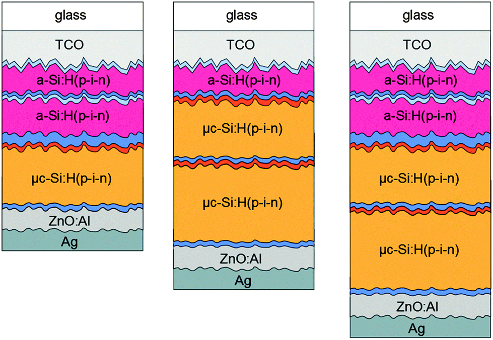 | ||
| Fig. 1 Schematic drawing of the a-Si:H/a-Si:H/μc-Si:H and a-Si:H/μc-Si:H/μc-Si:H triple and a-Si:H/a-Si:H/μc-Si:H/μc-Si:H quadruple junction solar cell structures in p–i–n configuration investigated in this study. | ||
| Cell type | Measured sub cell | |||
|---|---|---|---|---|
| Top cell | Middle cell 1 | Middle cell 2 | Bottom cell | |
| a-Si:H/μc-Si:H/μc-Si:H | 695 nm | 765 nm and 470 nm | — | 525 nm |
| a-Si:H/a-Si:H/μc-Si:H | 590 nm | 780 nm and 400 nm | — | 525 nm |
| a-Si:H/a-Si:H/μc-Si:H/μc-Si:H | 590 nm | 780 nm and 400 nm | 525 nm and 830 nm | 625 nm |
As an example, for the a-Si:H/μc-Si:H/μc-Si:H triple cell, light with 695 nm wavelength was used for the saturation of the middle and bottom cell assuring that the top cell, which photocurrent is intended to be measured, limits the current of the whole device. For the measurement of the bottom cell, light of 525 nm wavelength was used to saturate the top and the middle cell. In the case of the middle cell QE measurement, the top cell is saturated with a 470 nm light and the bottom cell is saturated with 765 nm light.
B. Photoelectrochemical measurements
The integrated PV-EC device is schematically depicted as band diagram illustration in Fig. 2. It is composed of four main components: the multijunction solar cell (p–i–n type photocathode) to provide sufficient photovoltage and photocurrent for the water splitting reactions, a catalyst layer to enhance the HER, which is deposited on top of the solar cell at the photocathode/electrolyte interface, the electrolyte, which should provide high ionic conductivity, and an anode, coated with a catalyst to enhance the OER. The photoelectrochemical performance of the PV-EC devices was evaluated at room temperature in aqueous 0.1 M and 1 M KOH solutions using a two-electrode configuration.34 The HER catalyst layer (Pt and Ni in this study) was deposited by electron beam evaporation with a thickness of around 150 nm on top of the Ag contact pads of the solar cell. In fact, the solar cell together with the attached HER catalyst compose the photocathode of the PV-EC device. The photocathode–electrolyte contact area was defined by an O-ring sealing aperture and was 0.5 cm2. For the OER catalyst, a RuO2 coated titanium sheet was used as anode (15 g m−2 RuO2, 3 cm2 active area, supplied by Metakem). Photocathode and anode were separated by a distance of 2 cm. White light photocurrent measurements were performed under simulated AM 1.5 solar illumination (100 mW cm−2) using an Oriel LCS-100 solar simulator (model 94011A) and an optical aperture of 0.5 cm2. Linear sweep voltammetry measurements were performed with a scan rate of 30 mV s−1 without stirring of the electrolyte. Electrical contact to the transparent conductive oxide (TCO) coated glass substrate, i.e. the front contact of the solar cell, was made by a silver paste. The PV-EC devices were illuminated through the glass substrate of the integrated solar cell (see Fig. 2), which offers the advantage that the light enters the photocathode through the TCO coated glass substrate without being attenuated by a surrounding medium (e.g. the electrolyte or gas bubbles). A major role in this configuration is governed by the metallic contact at the photocathode/electrolyte interface, which has to fulfill multiple requirements: (i) optical reflection of incident light back into the photocathode, (ii) protection of the photocathode from the electrolyte and undesired chemical reactions, and (iii) promotion of the catalytic reaction and a good electrical contact between the photocathode and the electrolyte. In this regard, a contact stack of ZnO:Al, Ag, and HER metal catalyst was used. The ZnO:Al/Ag double layer was used to ensure a good reflectivity of the incoming light, and thus allow for a high photocurrent. The thin metal layer deposited on top of the Ag layer was used as a catalyst for the HER.9,12,26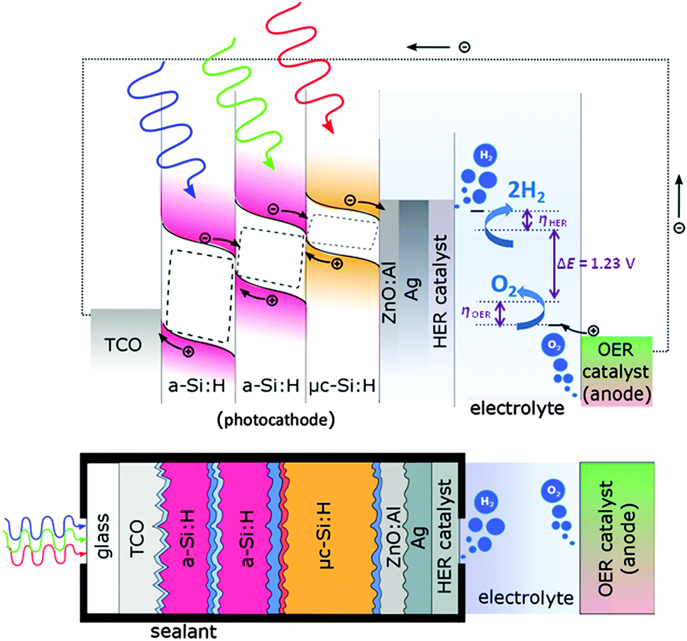 | ||
| Fig. 2 Band diagram illustration of the PV-EC device configuration investigated in this study, with its components: the multijunction photocathode (as example a-Si:H/a-Si:H/μc-Si:H) under non-biased illumination condition, a HER catalyst layer at the photocathode/electrolyte interface, the electrolyte, and the anode with the OER catalyst. The energy levels for the HER and OER and the respective reactions are indicated in the illustration. Hydrogen evolution occurs at the rear side of the photocathode and oxygen evolves at the anode side. ΔE = 1.23 V is the thermodynamic potential required for water electrolysis at 25 °C. ηHER and ηOER indicate the overpotentials for the HER and OER, respectively. | ||
Nevertheless, for industrial applications a two-compartment set-up for the OER and HER, respectively separated through a membrane for quantitative gas amount evaluation is desirable and currently under construction. The configuration used in this study particularly aims to test prototype PV-EC devices based on our developed solar cells.
III. Results and discussion
A. Multijunction solar cells
The development of individual sub cells (a-Si:H and μc-Si:H single junction solar cells) of a multijunction device has been addressed in detail elsewhere.9,26 The present study investigates the combination in triple and quadruple junction solar cells and exploits ways to improve the device efficiency in combination with high VOC ranging from 2.0 V to 2.8 V. Due to requirements on the band gap sequence, the top and bottom cell absorber layers were made of a-Si:H (high band gap) and μc-Si:H, respectively, for all investigated multijunctions. For the middle cell absorber layers in triple junction solar cells either a-Si:H (lower band gap) or μc-Si:H were applied, which leads to different voltage and current matching conditions and represents the two development paths discussed below.• a reference solar cell fabricated without μc-SiOx:H layers and without n–i buffer layer (“T1”),
• a cell with μc-SiOx:H layers for middle (〈n2〉) and bottom cell (〈n3〉) without n–i buffer layer (“T2”),
• the same cell as T2, but with 30 nm n–i buffer layer for the bottom cell (“T3”),
• the same cell as T2 with a 30 nm buffer layers for the bottom and a 20 nm thin buffer layer for the middle cell (“T4”).
Table 2 summarizes the performance of these triple junction cells, including layer preparation and PV parameters of the solar cells.
| Cell no. | μc-SiOx:H 〈n2〉 and 〈n3〉 layers | n–i buffer layer | V OC [mV] | J SC [mA cm−2] | FF [%] | V MPP [mV] | J MPP [mA cm−2] | η [%] |
|---|---|---|---|---|---|---|---|---|
| T1 | W/o | W/o | 1906 | 8.0 | 69.6 | 1598 | 6.6 | 10.6 |
| T2 | With | W/o | 1895 | 8.3 | 70.8 | 1602 | 6.8 | 11.1 |
| T3 | With | Bottom | 1958 | 8.3 | 68.1 | 1596 | 6.9 | 11.1 |
| T4 | With | Bottom and middle | 1976 | 8.4 | 67.6 | 1590 | 7.1 | 11.2 |
The sub cells had a thickness of 160 nm for the top, 1200 nm for the middle, and 1600 nm for the bottom cell. As presented in Table 2, the integration of μc-SiOx:H as intermediate reflecting layers effectively increased the photocurrent density by 0.4 mA cm−2 (T1 to T4). Through the integration of intrinsic a-Si:H buffer layers at the μc-Si:H n–i interfaces the VOC was increased by around 60 mV for one buffer layer (T3) and around 80 mV to 1976 mV for two buffer layers for middle and bottom cell (T4), along with a slight decrease in FF. Although the voltage at MPP was around 1.6 V for all cells, the current at MPP was increased by approx. 0.5 mA cm−2 from cell T1 to T4. Overall this result exemplarily demonstrates that the VOC can be tuned very systematically within a small voltage range, while the photocurrent at the MPP of the solar cell can be adjusted without impairing the device efficiency. This is relevant in particular for water splitting applications, as it allows to precisely adjust the PV parameters to the overpotential requirements of different catalyst materials.
Fig. 3 depicts the quantum efficiency measurement of the triple junction cell T4. The QE shows that all sub cells have very similar photocurrent densities of 8.0 mA cm−2, 8.2 mA cm−2, and 8.3 mA cm−2 as presented in Fig. 3.
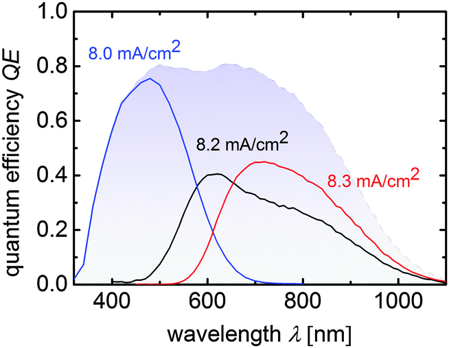 | ||
| Fig. 3 Quantum efficiency curves of a a-Si:H/μc-Si:H/μc-Si:H triple junction device corresponding to cell T4 from Table 2. Sub cell current densities calculated from the QE-curves are placed near the related measurements and the total QE is displayed by the blue shaded area. | ||
These values are slightly lower than the JSC value quoted in Table 2, where an anti-reflection foil was additionally used during J–V measurements. From the total QE photocurrent (shaded in blue) a slight dip between 500 nm and 650 nm is visible, which corresponds to reflection losses at the intermediate reflecting/absorber layer interface.
• a reference solar cell prepared without μc-SiOx:H n- and IR layers (“T5”),
• a cell with μc-SiOx:H n- and IR layers (“T6”), and
• the same cell as T6, but with adapted sub cell thicknesses such that a balanced maximum current level is provided by each sub cells (“T7”).
The experimental data of the triple junction cells, in terms of QE measured photocurrent densities of each individual sub cell, layer preparation (including layer thicknesses) and PV parameters are presented in Table 3.
| Cell no. | μc-SiOx:H 〈n1〉, IR, and 〈n3〉 | J QE,top [mA cm−2] (i-layer thickness [nm]) | J QE,mid [mA cm−2] (i-layer thickness [nm]) | J QE,bot [mA cm−2] (i-layer thickness [nm]) | V OC [mV] | J SC [mA cm−2] | FF [%] | V MPP [mV] | J MPP [mA cm−2] | η [%] |
|---|---|---|---|---|---|---|---|---|---|---|
| T5 | W/o | 7.3 (80) | 6.8 (400) | 7.4 (1200) | 2269 | 7.8 | 72.3 | 1859 | 6.9 | 12.8 |
| T6 | With | 7.4 (80) | 7.1 (400) | 7.4 (1200) | 2272 | 8.3 | 71.2 | 1860 | 7.1 | 13.4 |
| T7 | With (matched) | 7.6 (90) | 7.3 (700) | 7.6 (1800) | 2279 | 8.6 | 69.2 | 1851 | 7.4 | 13.6 |
Again, the JSC values are higher compared to the JQE values measured from the QE measurements because an anti-reflection foil was used for the J–V measurement. The integration of μc-SiOx:H n-layers and IR layers significantly enhanced JSC from 7.8 mA cm−2 (cell T5) to 8.3 mA cm−2 (cell T6), mainly due to the increase of the middle cell photocurrent density from 6.8 to 7.1 mA cm−2. The current matched cell T7 provided the highest JSC value of 8.6 mA cm−2 and a VOC of 2279 mV. This shows that our approach results in an increase in 0.8 mA cm−2 and 10 mV relative to cell T5. The good current-matching for cell T7 also results in the slightly decreased fill factor. Overall an efficiency of 13.6% was obtained along with a VMPP of 1851 mV with JMPP of 7.1 mA cm−2. Accordingly, in PV-EC device configuration, overpotential losses up to 600 mV (1.85–1.23 V), which is in the range of state-of-the-art precious metal catalyst materials for the HER and OER,38,39 are tolerable to operate the device near its maximum power point. The application of the multijunction solar cells in integrated water splitting device will be discussed in Section 3.2. The quantum efficiency measurement of cell T7 is shown in Fig. 4.
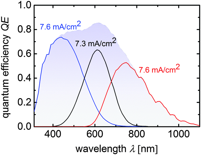 | ||
| Fig. 4 Quantum efficiency curves of a a-Si:H/a-Si:H/μc-Si:H triple junction device corresponding to cell T7 from Table 3. Sub cell current densities calculated from the QE-curves are placed near the related measurements. The blue shaded area displays the total QE of the triple junction solar cell. | ||
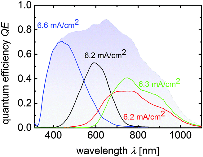 | ||
| Fig. 5 Quantum efficiency curves of the a-Si:H/a-Si:H/μc-Si:H/μc-Si:H quadruple junction solar cell. Sub cell current densities calculated from the QE-curves are placed near the related measurements and the total QE is displayed by the blue shaded area. | ||
In terms of water splitting, the high VMPP of around 2278 mV (JMPP = 5.8 mA cm−2) provides over 1 V of excess voltage and thus offers a lot of freedom in the choice of the catalyst material, which will be discussed in the following section.
Overall, the presented photovoltaic development deviates from prevalent routes, as we focused on high adjustable output voltages rather than on record electrical conversion efficiencies. Nevertheless, the conversion efficiencies of the triple and quadruple junction solar cells presented in this study are very close to the highest efficiencies reported for solar cells made of thin film silicon.43Fig. 6 summarizes the multijunction solar cell development and presents the J–V measurements of the best developed triple (cell T4 and T7 from Tables 2 and 3) and quadruple junction solar cells along with the VOC (2.0 V to 2.8 V) and VMPP (1.6 V to 2.3 V) range.
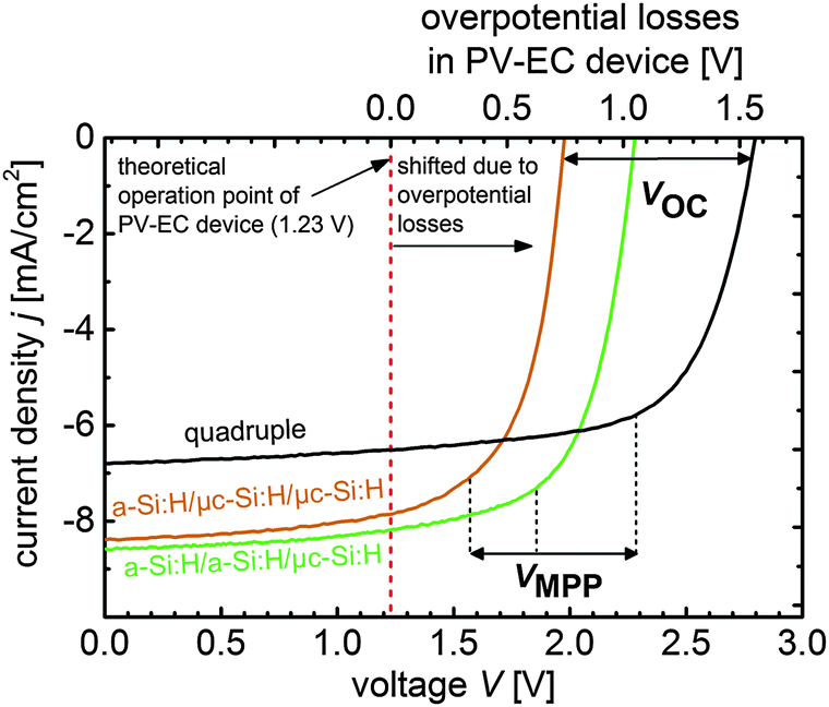 | ||
| Fig. 6 Current voltage curves of the developed triple, and quadruple junction solar cells based on a-Si:H and μc-Si:H. The achievable VOC (2.0 V to 2.8 V) and VMPP (1.6 V to 2.3 V) ranges are indicated, respectively. The J–V curves of the triple and quadruple junction solar cells are linked with the theoretical operation point of a PV-EC device at 1.23 V (red dashed vertical line, without overpotential losses). In real PV-EC devices this operation point is shifted due to overpotential losses, which are plotted on the upper x-axis. | ||
In real photoelectrochemical systems however, overpotential losses cause that the operation point (theoretically at 1.23 V, red vertical line in Fig. 6) is shifted towards more positive bias, as implied in Fig. 6. Assuming that all PV parameters of the solar cells remain unchanged when they are integrated in a PV-EC device, Fig. 6 allows to illustratively predict the performance of PV-EC devices based on our developed solar cells. The operation photocurrent density of a PV-EC device can be read at the crossing point of the solar cell J–V with the operation point line at the respective overpotential from the upper x-axis. As can be deduced from Fig. 6, the a-Si:H/a-Si:H/μc-Si:H triple junction could provide a maximum operation photocurrent density of 8.2 mA cm−2 when the PV-EC device would operate ideally, i.e. without any overpotential losses. When considering losses, the excess voltages become beneficial, as will be discussed in the following. Notwithstanding this, based on the presented photovoltaic results it is already possible to derive the practical performance limits of the state-of-the-art thin film silicon technology for water splitting applications.
B. Photovoltaic-biased electrosynthetic cells
 | (1) |
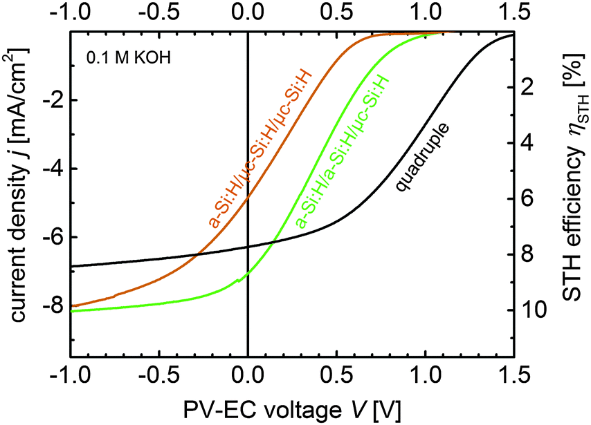 | ||
| Fig. 7 J–V measurements of PV-EC devices based on thin film silicon multijunction photocathodes with a 150 nm thick Pt layer as HER catalyst and a RuO2 counter electrode for the OER reaction. The measurements are conducted in 0.1 M KOH at 50 mV s−1. | ||
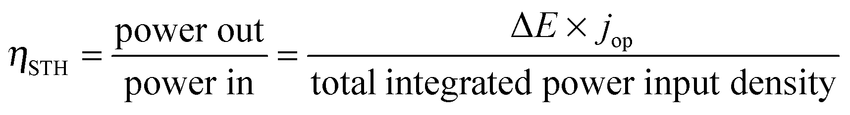
Above all, the measurements show that the highest photocurrent at 0 V applied bias is provided by the a-Si:H/a-Si:H/μc-Si:H based PV-EC device. The device operates near its MPP at 7.1 mA cm−2, which, according to eqn (1), corresponds to a STH efficiency of 8.7% in 0.1 M KOH. For the a-Si:H/μc-Si:H/μc-Si:H based device further improvements in the fill factor of the solar cell (cell T4) have to be made in order to reach the MPP photocurrent in the short-circuit condition, and thus, achieve a higher STH efficiency. The operation point of the quadruple junction device lies at 6.2 mA cm−2. Albeit the corresponding estimated 7.6% STH efficiency is lower compared to the a-Si:H/a-Si:H/μc-Si:H device for the respective catalysts, the quadruple junction device operates in a relatively flat region of the J–V curve (current plateau region). Hence, this device provides a certain excess voltage, which offers a higher flexibility in choosing other non-precious catalyst materials, as will be discussed in the following section. The experimental data of the three PV-EC devices are summarized in Table 4.
| Photocathode | j op [mA cm−2] | η STH [%] |
|---|---|---|
| a-Si:H/μc-Si:H/μc-Si:H | 4.8 | 5.9 |
| a-Si:H/a-Si:H/μc-Si:H | 7.1 | 8.7 |
| Quadruple | 6.2 | 7.6 |
In Fig. 8, the J–V measurements of the triple and quadruple junction based PV-EC devices with Pt and Ni layers as HER catalysts, respectively are compared.
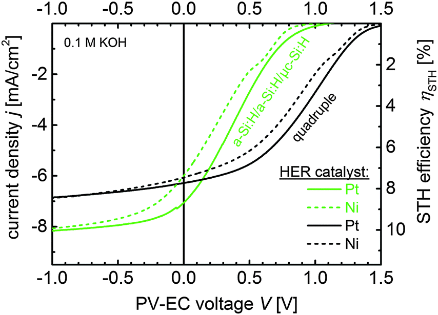 | ||
| Fig. 8 J–V measurements of PV-EC devices based on a-Si:H/a-Si:H/μc-Si:H triple and quadruple junction photocathodes with RuO2 counter electrode for the OER reaction. For the HER reaction 150 nm of Ni (dotted curves) and Pt (solid curves) were deposited on top of the solar cells, respectively. The measurements were conducted in 0.1 M KOH at 50 mV s−1. | ||
As expected, the operation photocurrent density jop for the Ni-coated triple and quadruple devices is lower compared to the platinized devices. But the a-Si:H/a-Si:H/μc-Si:H based device shows a significant decrease in jop from 7.1 to 6.1 mA cm−2, while the quadruple based device only loses 0.1 mA cm−2 by using a Ni catalyst layer instead of Pt and still operates in the current plateau region. Both Ni-coated devices exhibit nearly the same estimated STH efficiency of 7.5% in 0.1 M KOH. However, the operation point of the triple junction based device lies in the steep slope of its J–V characteristics, where a slight deterioration of the device parameters, due to photocorrosion during long-term operation for instance, can significantly deteriorate the STH efficiency. The operation point of the quadruple based device on the other hand lies in the plateau of its J–V characteristics, and thus, is less sensitive to photovoltage or fill factor variations.
 | ||
| Fig. 9 (a) Chronoamperometric stability measurement monitoring the long-term stability of the a-Si:H/a-Si:H/μc-Si:H and the quadruple junction based PV-EC devices with Pt and Ni catalyst layers, respectively, at 0 V applied bias on a logarithmic time scale. The measurements were conducted in 0.1 M (solid curves) and in 1 M KOH (dotted curves) under AM 1.5 illumination (100 mW cm−2). As a counter electrode for the OER reaction RuO2 was used. (b) J–V measurements of the triple and quadruple junction based PV-EC devices in 0.1 M (solid curves) and 1 M KOH (dotted curves). The measurements were conducted at a scan rate of 50 mV s−1. | ||
In 0.1 M KOH a stable photocurrent of approx. 6.1 mA cm−2 and 7.0 mA cm−2, respectively, was measured for both PV-EC devices over the course of 4 hours (approx. 15![[thin space (1/6-em)]](https://www.rsc.org/images/entities/char_2009.gif) 000 s). The periodical fluctuations in the photocurrent densities are caused by repetitive accumulation and detachment of H2 bubbles at the photocathode surface. The measurements in 1 M KOH revealed that both devices did not operate longer than 1000 s. This result shows that a relatively small change in the pH value from approx. 13 to 14 has a significant effect on the stability of the PV-EC devices. In particular, pitting corrosion and delamination of the stacked metal layers at the solar cell-electrolyte interface prevented longer operation times. Here, adapted PV-EC device designs for robust water splitting operations need to be considered.31
000 s). The periodical fluctuations in the photocurrent densities are caused by repetitive accumulation and detachment of H2 bubbles at the photocathode surface. The measurements in 1 M KOH revealed that both devices did not operate longer than 1000 s. This result shows that a relatively small change in the pH value from approx. 13 to 14 has a significant effect on the stability of the PV-EC devices. In particular, pitting corrosion and delamination of the stacked metal layers at the solar cell-electrolyte interface prevented longer operation times. Here, adapted PV-EC device designs for robust water splitting operations need to be considered.31
Notwithstanding this, in the case of the triple junction based device an increase of 0.7 mA cm−2 in the operation photocurrent density jop to 7.7 mA cm−2 is observed when 1 M KOH is used as electrolyte solution instead of 0.1 M KOH. From Fig. 9(b) it becomes apparent that this increase is caused by an improvement of the fill factor in the J–V curves of the triple junction based PV-EC devices. In fact, an increase in the electrolyte concentration reduces the series resistance of the complete PV-EC device, which leads to an improved fill factor. The effects of electrolyte resistance and other factors on the performance of PV-EC devices were investigated in more detail by modeling in a previous study.12 According to eqn (1) an impressive STH efficiency of 9.5% can be estimated from the jop of 7.7 mA cm−2 for the triple based PV-EC device with Pt as HER and RuO2 as OER catalyst. Please note that the solar-to-hydrogen efficiencies calculated viaeqn (1) represent an upper limit for the ηSTH due to the assumption of unity faradaic efficiency.
Referring to a recently published overview of demonstrated STH conversion efficiencies,11 this is the highest reported STH efficiency for an integrated monolithic thin film silicon based photoelectrochemical device. STH efficiencies over 10% would become feasible by using anti-reflection foils to enhance the saturation photocurrents of the a-Si:H/a-Si:H/μc-Si:H solar cell in the PV-EC device configuration by around 0.4 mA cm−2 from 8.2 to 8.6 mA cm−2 (see Fig. 6). However, the issue of photocorrosion, particularly present for electrolyte concentrations of or above 1 M, need to be solved at the same time. In this regard, the excess voltage provided by the quadruple junction based device offers an additional advantage. As apparent from Fig. 9(a) and (b), the increase in electrolyte concentration does not affect the operation photocurrent density of the device, which exhibits a jop of 6.1 mA cm−2 for the J–V measurements conducted 0.1 M and 1 M KOH, respectively. This result can be understood, because the device operates in the current plateau, where an improved fill factor does not improve the current density (see Fig. 9(b)). This overall shows that quadruple junction solar cells not only promote the usage of cheaper catalyst materials, but also allow for the operation in low-concentrated electrolytes without impairing the device efficiency, and thus, for an increased long-term stability of the device and the catalysts.
In total, the presented PV-EC device concept in combination with the broad range of tunable photovoltages offers an important toolbox for the investigation of related research challenges, including catalyst development,49 robust surface coating designs,30 or integrated device architectures.50
IV. Summary
The present study outlined the important steps towards designing highly efficient semiconductor structures and the presented results provide evidence that stable STH efficiencies over 10% are within the reach of thin film silicon based devices. We presented in detail the development of triple and quadruple junction solar cells based on a-Si:H and μc-Si:H and demonstrated their applicability for efficient solar water splitting. The series-connected multijunction cell configurations provided a wide range of achievable VOC (2.0 V to 2.8 V) and VMPP (1.6 V to 2.3 V) voltages. Additionally, we were able to systematically tune the VOC of the solar cells within a smaller voltage range (∼50 mV) without impairing the device efficiency, a feature which is highly important to compensate the losses occurring in photoelectrochemical applications. Overall, by carefully adjusting the photocurrents of the sub cells we achieved PV efficiencies of 13.6% for triple and 13.2% for quadruple junction solar cells. The application in PV-EC devices showed that the a-Si:H/a-Si:H/μc-Si:H based PV-EC device with Pt as hydrogen evolution catalyst and RuO2 as oxygen evolution catalyst exhibited 7.7 mA cm−2 at 0 V applied bias, which corresponds to a solar-to-hydrogen efficiency of 9.5% (assuming a 100% faradaic efficiency). The PV-EC device based on a quadruple junction cell (a-Si:H/a-Si:H/μc-Si:H/μc-Si:H) exhibited enough excess voltage to substitute Pt as precious metal catalyst by a more abundant material, such as Ni, and to work in low-concentrated electrolyte solutions without impairing the solar-to-hydrogen efficiency. With Ni as HER catalyst, this device provided 6.1 mA cm−2 at 0 V applied bias over the course of 4 hours.Conflict of interest
The authors declare no competing financial interests.Acknowledgements
We thank U. Gerhards, L. Petter, W. Reetz, and H. Siekmann, for their contributions to this work. The research is partly financially supported by the Deutsche Forschungsgemeinschaft (DFG) Priority Programme 1613 (SPP 1613): Regeneratively produced fuels by light-driven water splitting: Investigation of involved elementary processes and perspectives of technologic implementation, and by the German Bundesministerium für Bildung und Forschung (BMBF) in the network project: Sustainable Hydrogen (FKZ 03X3581A and FKZ 03X3581B). J. Ziegler, F. Yang, B. Kaiser, and W. Jaegermann acknowledge partial financial support by the DFG Excellence Graduate School of Energy Science and Engineering (GSC 1070).References
- T. R. Cook, D. K. Dogutan, S. Y. Reece, Y. Surendranath, T. S. Teets and D. G. Nocera, Chem. Rev., 2010, 110, 6474–6502 CrossRef CAS PubMed.
- C. A. Grimes, O. K. Varghese and S. Ranjan, Light, water, hydrogen: the solar generation of hydrogen by water photoelectrolysis, Springer, New York, 2008 Search PubMed.
- A. J. Nozik and R. Memming, J. Phys. Chem., 1996, 100, 13061–13078 CrossRef CAS.
- E. Miller, White Papers on Materials for Photoelectrochemical Water Splitting, DOE PEC Working Group, 2013 Search PubMed.
- Z. Li, W. Luo, M. Zhang, J. Feng and Z. Zou, Energy Environ. Sci., 2013, 6, 347–370 CAS.
- R. Memming, Semiconductor Electrochemistry, Wiley VCH, 2002 Search PubMed.
- A. C. Nielander, M. R. Shaner, K. M. Papadantonakis, S. A. Francis and N. S. Lewis, Energy Environ. Sci., 2015, 8, 16–25 CAS.
- B. Parkinson, Acc. Chem. Res., 1984, 17, 431–437 CrossRef CAS.
- F. Urbain, K. Wilken, V. Smirnov, O. Astakhov, A. Lambertz, J.-P. Becker, U. Rau, J. Ziegler, B. Kaiser, W. Jaegermann and F. Finger, Int. J. Photoenergy, 2014, 2014, 249317 CrossRef.
- F. F. Abdi, L. Han, A. H. M. Smets, M. Zeman, B. Dam and R. van de Krol, Nat. Commun., 2013, 4, 2195 Search PubMed.
- J. W. Ager, M. R. Shaner, K. A. Walczak, I. D. Sharp and S. Ardo, Energy Environ. Sci., 2015, 8, 2811–2824 CAS.
- F. Urbain, V. Smirnov, J.-P. Becker, U. Rau, J. Ziegler, B. Kaiser, W. Jaegermann and F. Finger, Sol. Energy Mater. Sol. Cells, 2015, 140, 275–280 CrossRef CAS.
- T. J. Mills, F. Lin and S. W. Boettcher, Phys. Rev. Lett., 2014, 112, 148304 CrossRef PubMed.
- Z. Huang, J. R. McKone, C. Xiang, R. L. Grimm, E. L. Warren, J. M. Spurgeon, H.-J. Lewerenz, B. S. Brunschwig and N. S. Lewis, Int. J. Hydrogen Energy, 2014, 39, 16220–16227 CrossRef CAS.
- A. E. Delahoy, S. C. Gau, O. J. Murphy, M. Kapur and J. O'M. Bockris, Int. J. Hydrogen Energy, 1985, 10, 113–116 CrossRef CAS.
- S. Y. Reece, J. A. Hamel, K. Sung, T. D. Jarvi, A. J. Esswein, J. J. H. Pijpers and D. G. Nocera, Science, 2003, 334, 645–648 CrossRef PubMed.
- V. Cristino, S. Berardi, S. Caramori, R. Argazzi, S. Carli, L. Meda, A. Tacca and C. A. Bignozzi, Phys. Chem. Chem. Phys., 2013, 15, 13083–13092 RSC.
- L. Han, I. A. Digdaya, T. W. F. Buijs, F. F. Abdi, Z. Huang, R. Lui, B. Dam, M. Zeman, W. A. Smith and A. H. M. Smets, J. Mater. Chem. A, 2015, 3, 4155–4162 CAS.
- R. E. Rocheleau, E. L. Miller and A. Misra, Energy Fuels, 1998, 12, 3–10 CrossRef CAS.
- O. Khaselev, A. Bansal and J. A. Turner, Int. J. Hydrogen Energy, 2001, 26, 127–132 CrossRef CAS.
- K. Fujii, S. Nakamura, M. Sugiyama, K. Watanabe, B. Bagheri and Y. Nakano, Int. J. Hydrogen Energy, 2013, 38, 14424–14432 CrossRef CAS.
- T. J. Jacobsson, V. Fjällström, M. Sahlberg, M. Edoff and T. Edvinsson, Energy Environ. Sci., 2013, 6, 3676–3683 CAS.
- C. R. Cox, J. Z. Lee, D. G. Nocera and T. Buonassisi, Proc. Natl. Acad. Sci. U. S. A., 2014, 111, 14057–14061 CrossRef CAS PubMed.
- J. Luo, J.-H. Im, M. T. Mayer, M. Schreier, M. Khaja Nazeeruddin, N.-G. Park, S. D. Tilley, H. Jin Fan and M. Grätzel, Science, 2014, 345, 1593–1596 CrossRef CAS PubMed.
- F. Finger, R. Carius, T. Dylla, S. Klein, S. Okur and M. Günes, IEE Proc., Part I: Solid-State Electron Devices, 2003, 150, 300–308 Search PubMed.
- F. Urbain, V. Smirnov, J.-P. Becker, U. Rau, J. Ziegler, B. Kaiser, W. Jaegermann and F. Finger, J. Mater. Res., 2014, 29, 2605–2614 CrossRef CAS.
- A. Lambertz, V. Smirnov, T. Merdzhanova, K. Ding, S. Haas, G. Jost, R. E. I. Schropp, F. Finger and U. Rau, Sol. Energy Mater. Sol. Cells, 2013, 119, 134–143 CrossRef CAS.
- S. Hu, M. R. Shaner, J. A. Beardslee, M. Lichterman, B. S. Brunschwig and N. S. Lewis, Science, 2014, 344, 1005–1009 CrossRef CAS PubMed.
- M. J. Kenney, M. Gong, Y. Li, J. Z. Wu, J. Feng, M. Lanza and H. Dai, Science, 2014, 342, 836–840 CrossRef PubMed.
- B. Mei, B. Seger, T. Pedersen, M. Malizia, O. Hansen, I. Chorkendorff and P. C. K. Vesborg, J. Phys. Chem. Lett., 2014, 5, 1948–1952 CrossRef CAS PubMed.
- N. A. Kelly and T. L. Gibson, Int. J. Hydrogen Energy, 2006, 31, 1658–1673 CrossRef CAS.
- W. Böttler, V. Smirnov, J. Hüpkes and F. Finger, Phys. Status Solidi A, 2012, 209, 1144–1149 CrossRef.
- C. Ulbrich, A. Gerber, K. Hermans, A. Lambert and U. Rau, Prog. Photovoltaics, 2013, 21, 1672–1681 Search PubMed.
- G. Hodes, J. Phys. Chem. Lett., 2012, 3, 1208–1213 CrossRef CAS PubMed.
- V. Smirnov, A. Lambertz, S. Tillmanns and F. Finger, Can. J. Phys., 2014, 92, 932–935 CrossRef CAS.
- S. Kirner, S. Calnan, O. Gabriel, S. Neubert, M. Zelt, B. Stannowski, B. Rech and R. Schlatmann, Phys. Status Solidi C, 2012, 9, 2145–2148 CrossRef CAS.
- S. Hänni, M. Boccard, G. Bugnon, M. Despeisse, J.-W. Schüttauf, F.-J. Haug, F. Meillaud and C. Ballif, Phys. Status Solidi A, 2015, 212, 840–845 CrossRef.
- L. C. Seitz, Z. Chen, A. J. Forman, B. A. Pinaud, J. D. Benck and T. F. Jaramillo, ChemSusChem, 2014, 7, 1372–1385 CrossRef CAS PubMed.
- C. C. L. McCrory, S. Jung, J. C. Peters and T. F. Jaramillo, J. Am. Chem. Soc., 2013, 135, 16977–16987 CrossRef CAS PubMed.
- J.-W. Schüttauf, B. Niesen, L. Löfgren, M. Bonnet-Eymard, M. Stuckelberger, S. Hänni, M. Boccard, G. Bugnon, M. Despeisse, F.-J. Haug, F. Meillaud and C. Ballif, Sol. Energy Mater. Sol. Cells, 2015, 133, 163–169 CrossRef.
- F. T. Si, D. Yun Kim, R. Santbergen, H. Tan, R. A. C. M. M. van Swaaij, A. H. M. Smets, O. Isabella and M. Zeman, Appl. Phys. Lett., 2014, 105, 063902 CrossRef.
- S. Kirner, S. Neubert, C. Schultz, O. Gabriel, B. Stannowski, B. Rech and R. Schlatmann, Jpn. J. Appl. Phys., 2015, 54, 08KB03 CrossRef.
- M. Green, K. Emery, Y. Hishikawa, W. Warta and E. D. Dunlop, Prog. Photovoltaics, 2015, 23, 1–9 Search PubMed.
- Z. Chen, T. F. Jaramillo, T. G. Deutsch, A. Kleiman-Shwarsctein, A. J. Forman, N. Gaillard, R. Garland, K. Takanabe, K. Heske, M. Sunkara, E. W. McFarland, K. Domen, E. Miller, J. A. Turner and H. N. Dinh, J. Mater. Res., 2010, 25, 3–16 CrossRef CAS.
- M. G. Walter, E. L. Warren, J. R. McKone, S. W. Boettcher, Q. Mi, E. A. Santori and N. S. Lewis, Chem. Rev., 2010, 110, 6446–6473 CrossRef CAS PubMed.
- Z. Chen, H. N. Dinh and E. Miller, Photoelectrochemical Water Splitting, Springer, New York, 2013 Search PubMed.
- R. H. Coridan, A. C. Nielander, S. A. Francis, M. T. McDowell, V. Dix, S. M. Chatman and N. S. Lewis, Energy Environ. Sci., 2015, 8, 2886–2901 CAS.
- J. R. McKone, E. L. Warren, M. J. Bierman, S. W. Boettcher, B. S. Brunschwig, N. S. Lewis and H. B. Gray, Energy Environ. Sci., 2011, 4, 3573–3583 CAS.
- K. Maeda and K. Domen, J. Phys. Chem. Lett., 2010, 1, 2655–2661 CrossRef CAS.
- B. Seger, I. E. Castelli, P. C. K. Vesborg, K. W. Jacobsen, O. Hansen and I. Chorkendorff, Energy Environ. Sci., 2014, 7, 2397–2413 CAS.
Footnote |
| † Electronic supplementary information (ESI) available. See DOI: 10.1039/c5ee02393a |
| This journal is © The Royal Society of Chemistry 2016 |