
Charge transport and mobility engineering in two-dimensional transition metal chalcogenide semiconductors
Song-Lin
Li
*a,
Kazuhito
Tsukagoshi
b,
Emanuele
Orgiu
*a and
Paolo
Samorì
*a
aInstitut de Science et d'Ingénierie Supramoléculaires (ISIS) and International Center for Frontier Research in Chemistry (icFRC), Université de Strasbourg and Centre National de la Recherche Scientifique (CNRS), Strasbourg 67083, France. E-mail: songlinli@gmail.com; orgiu@unistra.fr; samori@unistra.fr
bWorld Premier International Center for Materials Nanoarchitechtonics (WPI-MANA), National Institute for Materials Science (NIMS), Tsukuba, Ibaraki 305-0044, Japan
First published on 23rd November 2015
Abstract
Two-dimensional (2D) van der Waals semiconductors represent the thinnest, air stable semiconducting materials known. Their unique optical, electronic and mechanical properties hold great potential for harnessing them as key components in novel applications for electronics and optoelectronics. However, the charge transport behavior in 2D semiconductors is more susceptible to external surroundings (e.g. gaseous adsorbates from air and trapped charges in substrates) and their electronic performance is generally lower than corresponding bulk materials due to the fact that the surface and bulk coincide. In this article, we review recent progress on the charge transport properties and carrier mobility engineering of 2D transition metal chalcogenides, with a particular focus on the markedly high dependence of carrier mobility on thickness. We unveil the origin of this unique thickness dependence and elaborate the devised strategies to master it for carrier mobility optimization. Specifically, physical and chemical methods towards the optimization of the major factors influencing the extrinsic transport such as electrode/semiconductor contacts, interfacial Coulomb impurities and atomic defects are discussed. In particular, the use of ad hoc molecules makes it possible to engineer the interface with the dielectric and heal the vacancies in such materials. By casting fresh light on the theoretical and experimental studies, we provide a guide for improving the electronic performance of 2D semiconductors, with the ultimate goal of achieving technologically viable atomically thin (opto)electronics.
 Song-Lin Li | Song-Lin Li is currently a postdoctoral researcher at ISIS, University of Strasbourg, France. He earned his PhD degree (2009) from the Institute of Physics at the Chinese Academy of Sciences. He was a research associate (2009–2011) and an ICYS Fellow (2011–2014) at the International Center for Young Scientists (ICYS) at WPI-MANA, the National Institute for Materials Science (NIMS) in Tsukuba, Japan. He has worked on various research fields of materials science and physics, including nanoelectronics, reversible resistance switching effect, and superconductivity. His research interest now focuses on the electronic transport in two-dimensional materials and their (opto)electronic applications. |
 Kazuhito Tsukagoshi | Kazuhito Tsukagoshi is a Principal Investigator at WPI-MANA, NIMS, Japan, and group leader of the π-electron electronics group. He experienced experimental research on transport physics in semiconductor microstructures and completed his PhD degree (Osaka University) in 1995. Afterward, he worked as a visiting associate in the Cavendish Laboratory (University of Cambridge, UK) and then in Hitachi Cambridge Laboratory (Hitachi Europe Ltd, UK). In 1999, he joined RIKEN and undertook research on functional thin-film electronics. He continued his research in AIST in 2008 and moved to NIMS in 2009. His current interest focuses on atomically thin semiconductors and oxide field-effect transistors. |
 Emanuele Orgiu | Emanuele Orgiu is an Assistant Professor at the Faculty of Chemistry and permanent scientist at Institut de Science et d'Ingénierie Supramoléculaires (ISIS) at the University of Strasbourg. He holds a PhD in Physics of organic devices, earned in 2008 from the Università di Cagliari (Italy). He was a Fulbright scholar at the University of Santa Clara, CA, in 2007. In 2013, he was awarded the Technology Review Award – MIT Under35 for France. He works in the field of materials science and physics, with a focus on interfaces and transport in 2D materials and organic semiconductors and fabrication and characterization of nanodevices. |
 Paolo Samorì | Paolo Samorì is Distinguished Professor and director of the Institut de Science et d'Ingénierie Supramoléculaires of the Université de Strasbourg where he is also head of the Nanochemistry Laboratory. He is also a fellow of the Royal Society of Chemistry, a fellow of the European Academy of Sciences, a member of the Academia Europaea and a junior member of the Institut Universitaire de France (IUF). His past work was awarded various prizes, including the IUPAC Prize for Young Chemists (2001), the “Vincenzo Caglioti” Award (2006) granted by the Accademia Nazionale dei Lincei (Italy), the ERC Starting Grant (2010) and the CNRS Silver Medal (2012). |
1 Introduction
van der Waals (vdW) crystals represent a large family of materials that exhibit unique layered architectures, including graphite, metal oxides, chalcogenides, phosphates, and cuprates, which differ in their chemical composition and crystal structure, leading to markedly different properties, e.g. their electronic characteristics can span from metallic to insulating. These materials all share a common feature—large interlayer vdW spacings and weak interlayer interactions, which result in peculiar mechanical properties like interlayer sliding and cleavability. In prehistory (the 4th millennium B.C.) graphite, the most widely known vdW material, was used as pottery paint. Nowadays it is still an unbeatable component for day-to-day applications as pencil cores, motor electrodes, and dry lubricants. The characteristic layered structure also endows vdW materials intriguing chemical and physical properties which make them the building blocks of choice for intercalation chemistry,1 energy storage,2 and superconductivity.Remarkably, the structural anisotropy allows for mechanical exfoliation of vdW crystals down to the atomic scale.3–5 The two-dimensional (2D) vdW flakes such as monolayers of metal chalcogenides represent the thinnest manifestation of stable materials that exhibit an energy bandgap. Following the success of graphene,6,7 the research endeavor on 2D vdW semiconductors rapidly increased.8–36 The concurrence of several unique properties, including the atomic thickness, sizable bandgap, high carrier mobility and the absence of dangling bonds, and the fast-growing synthesis techniques37–78 pave the way towards revolutionary applications, such as ultimate atomically-thin-body field-effect transistors (FETs),79–82 stacked vdW superlattices and heterojunctions,83 valleytronics,84–89 and novel flexible and transparent electronics and optoelectronics.90–99 Here we will focus on the role of 2D vdW crystals as electroactive channels in FETs and, more specifically, on the factors influencing the electronic performances of the atomically-thin-body FETs and the devised strategies to improve them.
In fact, one of the prime interests in 2D crystals rests in their potential as conduction channels in digital circuits beyond silicon. The characteristic FET scaling length is derived as  ,100 where ε and t are electrical permittivity and thickness, and the subscripts s and ox denote semiconductor and oxide dielectric. The thinner the FET channels, the smaller and faster the FETs will be.101–103 Given the material physical limitation (such as surface roughness control) and production yield, the thickness of silicon channels can hardly be less than 5 nm,104 being much larger than the atomic scale. Exploiting 2D vdW semiconductors as FET channels would enable further device miniaturization after silicon.105,106
It is noteworthy that the 2D planar structure also offers full compatibility to conventional semiconductor processing such that they can be perfectly carved for making highly ordered FET arrays, being a critical factor rivaling the 1D nanostructures. The third figure of merit of the vdW semiconductors is the self-saturated nature of the surfaces which, in principle, contain no dangling bonds and are free of the composition fluctuation at the channel/dielectric interfaces, making them immune to the notorious ‘sixth-power law’ mobility degradation107 due to surface roughness (i.e. interface asperity) that occurs in non-vdW superlattices and silicon.108,109 The chemical stability is the fourth advantage which makes them stand out over other semiconductor membranes carved from 3D materials (e.g. silicene110 and germanene), which degrade rapidly under ambient conditions. In contrast, most vdW crystals are stable in air; some of them like graphite and molybdenite exist as minerals in nature.
In the framework of post-silicon microelectronics, great attention was initially devoted to the metallic graphene for its ultrahigh carrier mobility3–5 rather than 2D vdW semiconductors.111 It was then realized that it would be extremely difficult to use graphene for any digital application due to the absence of a bandgap, despite sustained efforts on bandgap and device engineering.112–125 Renewed interest on 2D vdW semiconductors arose in 2011 when Kis et al. reported high carrier mobility in monolayer MoS2 FETs.81,126
As far as the FET performance is concerned, one of the essential figures of merit is the field-effect mobility (μFE), which determines how fast a charge can move through a semiconductor or a metal under the effect of an external electric field. For 2D materials, where the surface and bulk structurally coincide, a major yet not fully unanswered question is why in such atomically thin semiconductors carrier mobility undergoes degradation4,111 unlike in the corresponding bulk systems,127 in spite of the immunity to the surface roughness scattering. It appears obvious that the full exposure of the lattice atoms to the environment can lead to strong carrier scattering and lower carrier mobility. In order to find out new strategies for improving carrier mobility, in-depth and quantitative answers to the thickness dependence of electronic performances are highly desirable.
Several theoretical studies were performed to cast light on the charge transport behavior of the 2D vdW semiconductors. Kaasbjerg et al. extensively investigated the role of lattice phonons in MoS2 monolayers and predicted an intrinsic transport mobility of ∼410 cm2 V−1 s−1 at room temperature.128,129 Jena et al. first considered the scattering generated by long-range Coulomb impurities in multilayer MoS2.130 Li et al. addressed the role of the channel thickness in carrier scattering by considering various scattering mechanisms and ascribed the interfacial impurity scattering as the origin of the strong thickness dependence of mobility.131 Alongside phonons and Coulomb impurities, Ma et al. were the first to consider the role of remote interface phonons, located in the dielectric, on the electronic behavior and identified the implications of using high-κ dielectric in atomically-thin-body MoS2 FETs.132 The above studies represent the theoretical framework of this review. On the other hand, a notable experimental effort was devoted to improving the mobility of 2D vdW flakes by (i) eliminating adverse extrinsic factors to attain material characteristics close to their intrinsic behavior, and (ii) upon strain engineering to gain extra performance enhancement. To date, dramatic progress has been achieved on the first route in particular through contact optimization and carrier scattering suppression.
The review will discuss the origin of the high thickness dependence of electronic performance exhibited by 2D vdW semiconductors, providing a theoretical insight and summarizing the devised strategies to minimize its effect. A brief introduction is first given in Section 1 to illustrate the advantages and current hurdles in using 2D vdW semiconductors as the active layer in FET devices. Section 2 outlines the material parameters regarding the electronic behavior, including the band structure, carrier effective mass, and lattice phonons. In order to provide the reader with information on the typical electronic properties of MX2 flakes, Section 3 gives an exhaustive list of the values of carrier mobility measured so far, together with fabrication and measurement details. The extrinsic and intrinsic factors responsible for the charge transport behavior are outlined in Section 4, shining light on the origin of the dependence of the electronic performances on thickness. Section 5 describes various physical and chemical strategies on mobility engineering developed in recent years, followed by the state-of-the-art performance achieved after mobility engineering. Section 6 presents the experimental standards one should follow to avoid experimental traps and unintentional errors, which are neglected in some literature. Finally, a summary and outlook on the above-mentioned research field are given that are meant to suggest new avenues to minimize the charge scattering while paving the way towards chemical strategies to be adopted.
2 Basic material properties
The term chalcogen was proposed around 1930 by Werner Fischer to denote the elements of Group 16. The use of such a term was approved in 1938 by the Committee of the International Union of Chemistry (later IUPAC).133 It was then widely accepted that the elements sulfur, selenium, and tellurium are named chalcogens whereas their compounds chalcogenides. A large number of chalcogenides exhibit a layered structure and lend themselves to the application as the conduction channels in FETs.In this section we outline the material parameters pertinent to electronic transport behavior in 2D vdW semiconductors, including crystal structure, phonon vibration mode, band structure, carrier effective mass, and electrical permittivity. Special attention is paid to the variation of these parameters with reducing material thickness, which may lead to mobility change.
2.1 Atomic structure
The metal chalcogenides’ chemical composition discussed in the review can be described by the formula MX2 (M = Ti, Zr, Hf, V, Nb, Ta, Cr, Mo, W, Pt and X = S, Se, Te). Fig. 1a displays the location of these elements in the element periodic table. The layered structure originates from the stacking of hexagonally packed X–M–X trilayer sandwich units. The metal and chalcogen atoms are covalently bonded as individual ‘tricomponent’ (trilayered) sandwich units while the different sandwich units are held together by a weak vdW force, resulting in a remarkably easy mechanical cleavage. In compliance with the terminology used in the literature, we call an individual ‘tricomponent’ sandwich unit as a MX2 monolayer. Within each layer, the atoms are arranged in configuration of either trigonal prism or octahedron (Fig. 1b), resulting in different lattice symmetries. It is worth noting that the layered structure is not only limited to the dichalcogenides composed of transition metal elements; some non-transition metal (e.g. Ga, In, Bi, Sn, and Pb) chalcogenides and halides also show layered structures. Fig. 1c illustrates some examples of monochalcogenides, trichalcogenides and halides that also possess a layered structure. Notably, Bi2Se3 and Bi2Te3 are well-known topological insulators.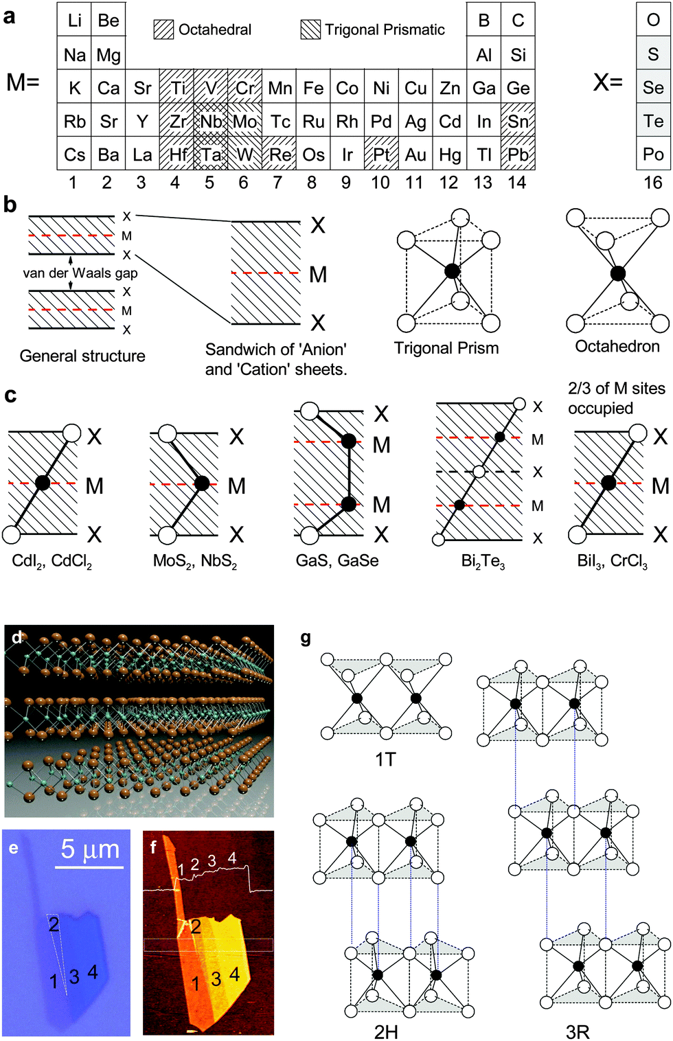 | ||
Fig. 1 (a) Element periodic table showing the metal and chalcogen elements that form the MX2 type van der Waals crystals. The shadows indicate the structure coordination of the crystals (octahedral or trigonal prismatic). Reproduced with permission from ref. 1, copyright 1978, Elsevier Ltd. (b) The two basic trigonal prismatic and octahedral coordination units for MX2 crystals. (c) Cross-sectional (along the 11![[2 with combining macron]](https://www.rsc.org/images/entities/char_0032_0304.gif) 0 plane) atomic coordination for MX2 chalcogenides and other typical van der Waals crystals. Panels (b) and (c) are reproduced with permission from ref. 8, copyright 1969, Taylor & Francis Ltd. (d) Three-dimensional schematic representation of a typical 2H-MX2 structure with the chalcogen atom X in yellow and the metal atom M in cyan. (e and f) Show optical and corresponding AFM images for a MoS2 flake with consecutive thickness values from 1 to 4 layers. Panels (e and f) are reproduced with permission from ref. 134, copyright 2012, American Chemical Society. (g) Schematic arrangements of sandwich units for the typical three phases of MoS2 crystals: 1T (tetragonal symmetry, one layer per repeat unit, octahedral coordination), 2H (hexagonal symmetry, two layers per repeat unit, trigonal prismatic coordination), and 3R (rhombohedral symmetry, three layers per repeat unit, trigonal prismatic coordination). The dotted vertical lines indicate the alignments of interlayer M and X atoms. 0 plane) atomic coordination for MX2 chalcogenides and other typical van der Waals crystals. Panels (b) and (c) are reproduced with permission from ref. 8, copyright 1969, Taylor & Francis Ltd. (d) Three-dimensional schematic representation of a typical 2H-MX2 structure with the chalcogen atom X in yellow and the metal atom M in cyan. (e and f) Show optical and corresponding AFM images for a MoS2 flake with consecutive thickness values from 1 to 4 layers. Panels (e and f) are reproduced with permission from ref. 134, copyright 2012, American Chemical Society. (g) Schematic arrangements of sandwich units for the typical three phases of MoS2 crystals: 1T (tetragonal symmetry, one layer per repeat unit, octahedral coordination), 2H (hexagonal symmetry, two layers per repeat unit, trigonal prismatic coordination), and 3R (rhombohedral symmetry, three layers per repeat unit, trigonal prismatic coordination). The dotted vertical lines indicate the alignments of interlayer M and X atoms. | ||
Due to compositional variation, the MX2 family covers a wide range of electronic properties, spanning from those of an insulator like HfS2, to semiconductors like MoS2 and semi-metals like WTe2 and TeS2, way down to true metals like NbS2 and VSe2.8 In this review article we focus our attention on semiconductors with a bandgap at around 1–2 eV. As a prototype MX2 semiconductor, we will especially concentrate on the structure and properties of MoS2 layers. Fig. 1d shows the atomic structure for typical 2H-phased MoS2. It exists in nature as the mineral molybdenite and can be easily mechanically exfoliated into few-layer flakes. Fig. 1e and f illustrate the optical and atomic force images for an exfoliated MoS2 flake with consecutive numbers of layers (NL, N is an integer) from 1 to 4. In fact, MoS2 has three different structural phases: 1T (tetragonal symmetry), 2H (hexagonal symmetry) and 3R (rhombohedral symmetry), as illustrated in Fig. 1g. Among them, the 2H and 3R phases are semiconducting while the 1T phase is metallic. Phase change can occur under external stimuli135,136 or chemical treatment,137–139 for example, by soaking in n-butyl lithium MoS2 can undergo phase change from semiconducting 2H to metallic 1T phase. The phase change induced property change has been employed to reduce the contact resistance, as will be discussed in Section 5.
2.2 Lattice phonon modes
In elastic materials the lattice phonon is a collective atom displacement with atoms vibrating around their equilibrium positions. Such a displacement can modify the carrier pathway in two ways: (1) deformation of the local lattice potential and (2) formation of electric fields due to polarizability and piezoelectricity of lattices. These two scattering mechanisms will be discussed in Section 4.2. Lattice phonons have a thermal origin and exist at non-zero temperatures; hence, unlike other scattering centers phonon is an intrinsic scattering factor.The phonon modes of bulk MX2 vdW crystals have been fully investigated in the 1970–1980s. Related information such as symmetry representation, vibration mode, and optical activity are well documented in the literature.141–151 Taking advantage of the capacity to reduce the thickness of the crystal, new information such as frequency shift152 and excitation of new phonon modes153,154 has been acquired in recent years.
According to the frequency–momentum (ω–k) dispersion relations, phonons are categorized into two types: acoustic (ω ∝ k at k ≈ 0) and optical (ω ≈ constant), which represent the relative motion phase for adjacent atoms. A simple rule to discern the phonon feature, for instance in a 1D diatomic chain, is that the optical modes are produced when two adjacent atoms move against each other (out-of-phase), while the acoustic modes are produced when they move together (in-phase). Fig. 2a and b show the calculated dispersion relations for the MX2 monolayer and bulk, respectively. Specifically, for the monolayer MX2 one unit cell comprises one X–M–X sandwich with 3 atoms and thus there are 9 phonon modes (3 acoustic and 6 optical modes). The number of atoms in the unit cell increases to 6 for bulk and, accordingly, the number of optical modes increases to 15.
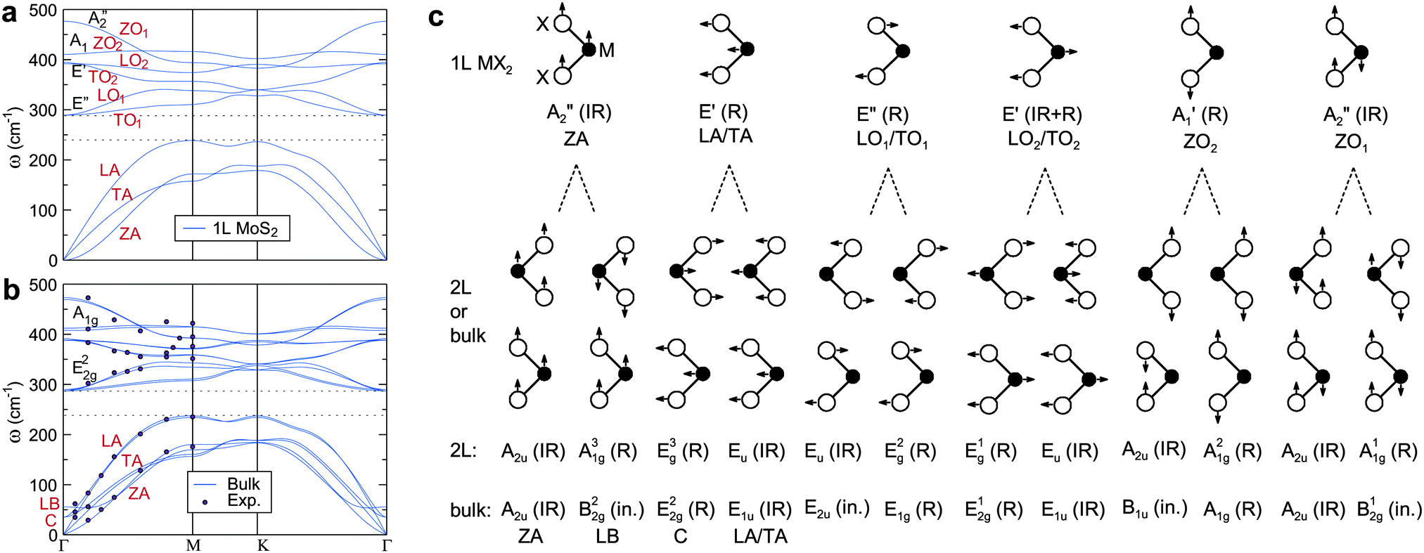 | ||
| Fig. 2 Calculated phonon dispersion curves for (a) 1L and (b) bulk MoS2. The dots in (b) are the data from inelastic neutron scattering experiments. Panels (a) and (b) are reproduced with permission from ref. 140, copyright 2011, American Physical Society. (c) Vibration modes, symmetry representation, and optical activities (Raman: R; Infrared: IR; inactive: in.) of the lattice phonons for 1L, 2L and bulk MX2. There are 6 optical and 3 acoustic branches in the 1L flake while the numbers of optical branches increase to 3 × 6 − 3 = 15 for 2L and bulk samples, due to the doubling of the numbers of atoms in unit cells. Note that the low-frequency LB and C modes are of optical characteristics although they share quite close dispersion behavior to the 3 acoustic modes at high wavenumbers. Reproduced with permission from ref. 35, copyright 2015, Royal Society of Chemistry. | ||
Fig. 2c illustrates the schematic atomic vibration modes, optical activities (Raman, infrared, or inactive, abbreviated here as R, IR and in., respectively), and acoustic/optical features for the monolayer (1L), bilayer (2L) and bulk MoS2. Lattice vibration modes are normally classified according to the irreducible representation of the crystal symmetry. For few-layer flakes, the symmetries differ if the flakes have an odd or even number of layers. The odd numbered flakes have a point group symmetry of D3h owing to the presence of the horizontal reflection plane (σh) that passes through the transition metal atom (M). The corresponding representation is Γ = 2A2′′ + A1′ + 2E′ + E′′,155,156 where one A2′′ and one E′ are acoustic modes, another A2′′ is IR active, A1′ and E′′ are R active, and another E′ is both R and IR active, as shown in Fig. 2a. In contrast, due to the presence of the inversion symmetry, the symmetry of the even numbered flakes is D3d with the representation: Γ = 3A1g + 3A2u + 3Eg + 3Eu,157,158 where one A2u and one Eu are acoustic modes, the other A2u and Eu are IR active, and A1g and Eg are R active.
For bulk MX2, the point group symmetry is enhanced to D6h due to the gain of translational symmetry along the z axis.157 The lattice vibrations at Γ point is: Γ = A1g + 2A2u + 2B2g + B1u + E1g + 2E1u + 2E2g + E2u,141,156 where one A2u and one E1u are acoustic modes, A1g, E1g, and E2g are R active, another A2u and E1u are IR active, and B2g, B1u, and E2u are optically inactive. Here the modes denoted by the letter “E” are doubly degenerate in the xy plane. For the sake of clarity, Table 1 also lists the crystal symmetry, vibration mode, and Raman frequency for the 1L, 2L and bulk MoS2.
| D 3h | D 3d/D6h | Activity | Direction | Atoms | ω MoS2 (cm−1) | |
|---|---|---|---|---|---|---|
| A2′′ (IR) | A2u/A2u | IR | z axis | Mo + S | 0.0 | 0.0 |
| A31g/B22g | R/in. | 55.7 | ||||
| E′ (R) | E3g/E22g | R | xy plane | Mo + S | — | 35.2 |
| Eu/E1u | IR | — | ||||
| E′′ (R) | Eu/E1u | IR/in. | xy plane | S | 289.2 | 287.1 |
| E2g/E1g | R | 288.7 | ||||
| E′ (IR + R) | E1g/E12g | R | xy plane | Mo + S | 391.7 | 387.8 |
| Eu/E1u | IR (E⊥z) | 391.2 | ||||
| A1 (R) | A2u/B1u | IR/in. | z axis | S | 410.3 | 407.8 |
| A21g/A1g | R | 412.0 | ||||
| A2′′ (IR) | A2u/A2u | IR (E∥z) | z axis | Mo + S | 476.0 | 469.4 |
| A11g/B12g | R/in. | 473.2 | ||||
2.3 Band structure and electrical permittivity
When compared to bulk materials, the band structures of 2D materials are considerably modified due to the quantum confinement effect. The energy–momentum relation (of electrons) and even the positions of band edges can be altered that can lead to a fundamental change of physical properties such as carrier effective mass and dielectric constant, which requires a special attention when comparing the performances of the same material measured at different thicknesses.In particular, two aspects are closely related to the charge transport. First, the bandgap magnitude determines the height of the Schottky barrier at the semiconductor/electrode interface. For MoS2 carrier injection into the monolayer is more difficult than into bulk owing to a broader bandgap, whereas the trend is opposite for black phosphorus that has a narrower bandgap in monolayer. Second, the effective mass m* directly reflects the intrinsic mobility following the equation μ ∝ 1/m*. Kuc et al. calculated the band structures for MoS2 with different thickness values from 1L to bulk and systematically revealed the influence of thickness on the position of band edges as well as the size of the bandgap.159Fig. 3 shows the band structures of bulk, 2L and 1L MoS2, with the band edges of the valence and conduction bands indicated by arrows. For 2L and bulk MoS2 the conduction band minimum and the valence band maximum are located at the Γ point and a midpoint between K and Γ, respectively. Both of them shift to the K point for the 1L MoS2. The energy–momentum relations at different values of the momentum are not necessarily the same and thus the shift in the conduction band minimum may change the carrier effective mass and the intrinsic mobility. Table 2 lists the thickness modulated carrier effective mass values in MoS2 calculated by Yun et al.160 Evidently, the electron effective mass is reduced from 0.551 to 0.483 me as MoS2 is thinned from bulk to 1L, where me is the electron mass. The slight reduction of carrier effective mass is favorable to achieving high mobility.
 | ||
| Fig. 3 Band structures of bulk, bilayer, and monolayer MoS2. The top of the valence band and the bottom of the conduction band are highlighted in green. The red arrows indicate the smallest value of the bandgap (direct or indirect) for a given thickness. Adapted with permission from ref. 159, copyright 2011, American Physical Society. | ||
| Type | Symmetry point | Bulk | 2L | 1L |
|---|---|---|---|---|
| Hole | Γ | 0.711 | 1.168 | 3.524 |
| K | 0.625 | 0.628 | 0.637 | |
| Electron | Midpoint of Γ–K | 0.551 | 0.579 | 0.569 |
| K | 0.821 | 0.542 | 0.483 |
Also, reducing thickness by exfoliating the top layers changes the electrostatic surroundings of the remaining low lying layers and, consequently, may alter the carrier screening and electrical permittivity (dielectric constant, ε), forming a third way to modify charge transport. Fig. 4 summarizes theoretical and experimental values of dielectric constants for MoS2 at different thicknesses. In theoretical studies, monotonic thickness dependence of ε is generally traced. Using first-principles calculation, Kumar et al. theoretically studied the influence of thickness on the dielectric properties (in-plane ε∥ and out-of-plane dielectric constant, ε⊥) of Mo and W based chalcogenides.161 In their calculation, both ε∥ and ε⊥ decrease as thickness reduces. For instance, ε⊥ of MoS2 is reduced from 12.8 to 4.8 when thinned from bulk to the monolayer. However, it should be noted that even for a specific sample large discrepancies still exist among different theoretical research groups, which results in tremendous variation in adopting the ε value when calculating the field-effect mobility. Taking the 1L MoS2 as an example, Yoon et al. use 3.3 in their non-equilibrium Green's function calculation,162 while Li et al. adopt 17.8 following the value of bulk,131 and Ma et al. employ 7.6.132 Therefore, more accurate measurements or techniques that can lead to more reliable permittivity information need to be developed.
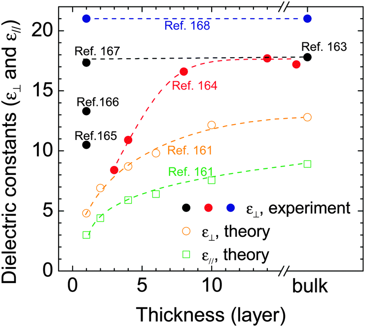 | ||
| Fig. 4 Theoretical and experimental values of dielectric constants for MoS2 at different thicknesses. While most theoretical calculations favor the increasing trend of dielectric constant with increasing thickness, there are controversies in experiments on the trend of dielectric constant with thickness. | ||
The electrical permittivity can be determined experimentally by optical absorption and reflection techniques.163–168 Several groups have measured the ε in thick MoS2 with different thicknesses. The data from Yim et al.164 seem to support the reducing trend of ε upon reducing thickness as predicted theoretically by Kumar et al., but the magnitudes are generally higher. On the other hand, owing to the influence of surface adsorbate layers on the ultrathin samples (e.g. water and chemical residues on substrates), inconsistent experimental results were reported for the monolayer MoS2, with the real part of static ε varying from 10.5 to 21.164–168 Among them, Li et al. measured a ε⊥ value of 17.3 in monolayer MoS2,167 being quite close to the bulk value of 17.8 reported by Hughes et al.163 If these values are reliable, it would imply no variation of the dielectric permittivity with reducing thickness. This conclusion is further supported by the optical reflectance measurements from Heinz et al. where they observed nearly similar ε⊥ between bulk and the monolayer in all the visible regime for four types of MX2 (MoS2, MoSe2, WS2, and WSe2).168 As it will be discussed in Section 4, ε determines the polarization function as well as the frequency and the coupling intensity of the surface polar phonon, which is an essential parameter for studying the carrier scattering mechanisms. Reliable information on electrical permittivity is instrumental to gain more accurate understanding on the electronic transport behavior.
3 Electronic performance at early times (with slight or without mobility engineering)
For 2D chalcogenides, their charge transport behavior is more susceptible to lattice defects and external surroundings (e.g. gaseous adsorbates from air and trapped charges in substrates) due to the fact that the surface and bulk coincide. In experiment, a wide distribution of carrier mobility exists as a result of varied sample quality and measurement conditions. Table 3 lists typical carrier mobility values of MX2 chalcogenides reported in recent years. In order to find out the relationship between carrier mobility and extrinsic factors (contact quality, densities of charged impurities and structural defects), a detailed device information, when available, is also outlined in the table, including preparation methods (exfoliated or synthesized), channel thickness, contact metals, thermal annealing conditions (in situ or ex situ, gas environment, temperature, and duration), interface surroundings, and measurement environment.| Channel material | Channel thickness | Contact and doping | Thermal annealing | Dielectric and encapsulation | Measurement pressure | μ near RT cm2 V−1 s−1 | μ at LT cm2 V−1 s−1 | γ value near RT | Ref. |
|---|---|---|---|---|---|---|---|---|---|
| Abbreviations and notes. C: chemical vapour deposition (CVD), A: atmospheric pressure CVD (APCVD), M: metal–organic CVD (MOCVD), S: sputtering. p: p-type conduction, NL: number of layers (N is an integer). ex.: ex situ, in.: in situ, vac.: vacuum, PPMS: physical property measurement system, RT: room temperature, LT: low temperature. BG: bottom gated, TG: top gated, DE: double-side encapsulated, BC: bottom contacted, IL: ionic liquid, IG: ionic gel, Gr.: graphene. + (annealing): in situ annealing is also used besides ex situ annealing. X → Y: experimental conditions (or mobility) change from X to Y. ?: mobility value deserves to be checked due to top/bottom gate coupling. 4W: 4-wire measurement. | |||||||||
| MoS2 | 1L | Au | TG:Al2O3 | 80 (?) | 93 | ||||
| MoS2 | 1L | Ti | in. 0.7 Pa 300 °C 1 h | TE:Si3N4 | Humidity | 71.8 (?) | 169 | ||
| MoS2 | 1L | Au | BG:SiO2 | 64 | 147 (6.5 K) | 170 | |||
| MoS2 | 1L | Au | ex. Ar/H2 200 °C 2 h | BG:SiO2 | ∼0.13 mPa | 594W | 171 | ||
| +in. 120 °C 12 h | 171 | ||||||||
| MoS2 | 1L | Ti | ex. Ar/H2 350 °C 3 h | BG:SiO2 | ∼0.13 mPa | ∼20Hall | 250 (4 K) | 1.7 | 172 |
| MoS2 | 1L | Au/IL | ex. 200 °C 2 h | TG:IG | vac. | 230 (10 K) | 1.22 | 173 | |
| MoS2 | 1L | Mo | 147 °C 2 h | BG:Al2O3 | 11–13 | 174 | |||
| MoS2 | 1L | Ti | ex. vac. 200 °C | BG:SiO2 → BN | 0.5 → 7.6–12 | 175 | |||
| MoS2 | 1L | Au | ex. N2 250 °C 1 h | BG:SiO2 | ∼1 | 176 | |||
| MoS2 | 1L | Au | ex. N2 250 °C 1 h | →BG:BN | →∼10 | 176 | |||
| MoS2 | 1L | Ti | BG:SiO2 | vac. | 1.1–10 | 169 | |||
| MoS2 | 1L | Cr | Suspended | ∼0.13 mPa | 0.9 | 177 | |||
| MoS2 | 1L | Cr | BG:SiO2 | ∼0.13 mPa | 0.1 | 177 | |||
| MoS2 | 1L | Cr | Suspended | 0.05 | 178 | ||||
| MoS2 | 2L | Ti | in. 120 °C 20 h | BG:SiO2 | ∼0.13 mPa | ∼80Hall | 375 (3 K) | 1.1 | 172 |
| MoS2 | 2L | Au | ex. 200 °C 2 h | TG:IG | vac. | 450 (2 K) | 1.9–2.9 | 173 | |
| MoS2 | 2L | Ti | No | BG:SiO2 | vac. | 35 | 179 | ||
| MoS2 | 2L | Au | ex. Ar/H2 200 °C 2 h | BG:SiO2 | ∼0.13 mPa | 334W | 171 | ||
| +in. 120 °C 12 h | 171 | ||||||||
| MoS2 | 2L | Au | ex. N2 250 °C 1 h | BG:BN | ∼27 | 176 | |||
| MoS2 | 2L | Au | TG:Al2O3 | 27 | 93 | ||||
| MoS2 | 2L | Ti | ex. vac. 200 °C | BG:SiO2 | ∼7 | 175 | |||
| MoS2 | 2L | Ti | ex. vac. 200 °C | →BG:BN | →24 | 175 | |||
| MoS2 | 2L | Mo | 147 °C 2 h | BG:Al2O3 | 11–14 | 174 | |||
| MoS2 | 2L | Au | ex. N2 250 °C 1 h | BG:SiO2 | ∼3.5 | 176 | |||
| MoS2 | 2L | Ti | in. vac. 77 °C | BG:SiO2 | ∼0.13 mPa | 4 | 180 | ||
| MoS2 | 2L | Ti | ex. Ar/H2 400 °C | BG:SiO2 | Air | 0.12 | 180 | ||
| MoS2 | 2–3L | Au → 1T | No | BG:SiO2 | Air | 19 → 46 | 137 | ||
| MoS2 | 2–3L | Au → 1T | No | TG:HfO2 | Air | 3.5 → 12.5 | 137 | ||
| MoS2 | 2 nm | Sc | BG:SiO2 | 26 | 181 | ||||
| MoS2 | 3L | Au | ex. 200 °C 2 h | TG:IG | vac. | 65–95 | 820 (2 K) | 1.9–2.4 | 173 |
| MoS2 | 3L | Ti | TG:IL | ∼0.13 mPa | 63 | 182 | |||
| MoS2 | 3L | Ti | ex. vac. 200 °C | BG:SiO2 | ∼9 | 175 | |||
| MoS2 | 3L | Ti | ex. vac. 200 °C | →BG:BN | →45 | 175 | |||
| MoS2 | 3L | Au | ex. Ar/H2 200 °C 2 h | BG:SiO2 | ∼0.13 mPa | 364W | 171 | ||
| +in. 120 °C 12 h | 171 | ||||||||
| MoS2 | 3L | Mo | 147 °C 2 h | BG:Al2O3 | ∼27 | 174 | |||
| MoS2 | 3L | Ni | TG:ZrO2 | 25 | 183 | ||||
| MoS2 | 3L | Permalloy | in. 87 °C 2 h | BG:SiO2 | vac. | ∼27 (200 K) | ∼54 (2 K) | ∼0.6 | 184 |
| MoS2 | 3L | Ni | TG:IG | 12 | 185 | ||||
| MoS2 | 3L | Au | TG:Al2O3 | 10 | 93 | ||||
| MoS2 | 3–5L | Cr | TG:Y2O3/HfO2 | 47.7 ± 11.9 | 186 | ||||
| MoS2 | 3–5L | Cr | TG:Al2O3/HfO2 | 37.4 ± 11.4 | 186 | ||||
| MoS2 | 3–5L | Cr | TG:MgO/HfO2 | 15.9 ± 7.2 | 186 | ||||
| MoS2 | 4L | Mo | 147 °C 2 h | BG:Al2O3 | 22–26 | 174 | |||
| MoS2 | 4L | Ti | ex. vac. 200 °C | BG:SiO2 | ∼5 | 175 | |||
| MoS2 | 4L | Ni | BG:SiO2 | vac. | 310 (1 K) | 187 | |||
| MoS2 | 5L | Mo | 147 °C 2 h | BG:Al2O3 | 25–26 | 174 | |||
| MoS2 | 5L | Ti | ex. vac. 200 °C | BG:SiO2 | ∼15 | 175 | |||
| MoS2 | 5L | Ti | BG:SiO2 | ∼0.13 mPa | ∼5 (295 K) | ∼0.3 (140 K) | 182 | ||
| MoS2 | 5L | Ti | TG:IL | ∼0.13 mPa | ∼100 (180 K) | ∼220 (77 K) | 1 | 182 | |
| MoS2 | 6L | Au | No | BG:SiO2 | vac. | 49 | 179 | ||
| MoS2 | 6L | Ti | No | BG:SiO2 | vac. | 42 | 179 | ||
| MoS2 | 5 nm/7L | Ti | BG:SiO2 | ∼0.13 mPa | ∼75 (295 K) | ∼180 (140 K) | 182 | ||
| MoS2 | 5 nm | Ni or Au | No | BG:SiO2 | 28 | 188 | |||
| MoS2 | 5–6 nm | Ni | BG:SiO2 | vac. | 24 | 187 | |||
| MoS2 | 8 nm | Ti | BG:SiO2 | ∼0.13 mPa | ∼40 (300 K) | ∼390 (77 K) | 1.7 | 182 | |
| MoS2 | 8 nm | Ti | TG:IL | ∼0.13 mPa | ∼160 (100 K) | ∼390 (77 K) | 1.2 | 182 | |
| MoS2 | ∼10 nm | Sc | BG:SiO2 | 184 | 181 | ||||
| MoS2 | ∼10 nm | Ti | BG:SiO2 | 125 | 181 | ||||
| MoS2 | ∼10 nm | Ni | BG:SiO2 | 36 | 181 | ||||
| MoS2 | ∼10 nm | Pt | BG:SiO2 | 21 | 181 | ||||
| MoS2 | 10 nm | BLG | in. 200 °C 3 h | TG:BN | 26, 33(no Rc) | 189 | |||
| MoS2 | 10 nm | Ti | TG:IL | 44Hall (220 K) | 190 | ||||
| MoS2:p | 86Hall (220 K) | 190 | |||||||
| MoS2 | 11 nm | Ti | BG:SiO2 | 8.4 | 191 | ||||
| MoS2 | 11 nm | Ti | TG:Al2O3 | 9.8 | 191 | ||||
| MoS2 | 1–17 nm | Cr | As-fabricated | Suspended | vac. | 0.01–46 | 192 | ||
| MoS2 | 1–17 nm | Cr | ex. Ar/H2 200 °C 1 h | Suspended | vac. | 0.5–105 | 192 | ||
| MoS2 | 12 nm | Ti | ex. Ar/H2 200 °C 2 h | BG:SiO2 | vac. (PPMS) | ∼1504W | 193 | ||
| MoS2 | 12 nm | Ti | ex. Ar/H2 200 °C 2 h | BG:SiO2 | vac. (PPMS) | 91 | 193 | ||
| MoS2 | 13 nm | Co → 1 nm TiO2 | BG:SiO2 | vac. | 12 → 76 | 194 | |||
| MoS2-M | 1L | Ti/Au | BG:SiO2 | AmbientRT | 3–37all | 90–110 (90 K) | 1.6 | 78 | |
| MoS2-M | 1L | Ti/Au | BG:SiO2 | vac.LT | 25–35best | 78 | |||
| MoS2-C | 1L | Ag | DE:Si3N4 | ∼0.13 mPa | 24 | 58 (77 K) | 0.65 | 195 | |
| TG:HfO2 | 195 | ||||||||
| MoS2-C | 1L | Ti | BG:–SH | <1.3 mPa | 13 | 196 | |||
| MoS2-C | 1L | Ti | 200 °C | TG:Al2O3 | 11 ± 3 | 197 | |||
| MoS2-S | 1L | Cr | BG:SiO2 | 7 (2–12) | 75 | ||||
| MoS2-C | 1L | Ti | TG:HfO2 | 6, 30band | 1.3, 13band (50 K) | 198 | |||
| MoS2-C | 1L | Ti | ex. Ar/H2 350 °C 2 h | BG:SiO2 | 3.6 | ∼3.6 (90 K) | 74 | ||
| MoS2-C | 1L | Ti | BG:–NH2 | <1.3 mPa | 3.6 | 196 | |||
| MoS2-C | 1L | Ti | BG:SiO2 | <1.3 mPa | 1.9 | 196 | |||
| MoS2-A | 1L | Ti | BG:SiO2 | ∼1.3 mPa | 1.2 | 52 | |||
| MoS2-C | 2L | Ti | ex. Ar/H2 350 °C 2 h | BG:SiO2 | 8.2 | ∼8.2 (90 K) | 74 | ||
| MoS2-C | 2–3L | 1T MoS2 | No | BG:SiO2 | Air | 24 → 56 | 138 | ||
| MoS2-C | 3L | Ti | ex. Ar/H2 350 °C 2 h | BG:SiO2 | 15.6 | ∼15.6 (90 K) | 74 | ||
| MoS2-C | 5.7 nm | Ti/Ni | BG:SiO2 | 9.9 | 199 | ||||
| MoS2-C | 70 nm | Ti/Ni | BG:SiO2 | 42 | 199 | ||||
| MoSe2-C | 1L | Ti | ex. vac. 120 °C 2 h | BG:SiO2 | 50 | 61 | |||
| MoSe2 | Few nm | Ni | BG:SiO2 | ∼13 μPa | ∼40 | 180 (78 K) | 2.1 | 200 | |
| MoSe2 | 7 nm | Ti | ex. Ar/H2 250 °C 2 h | BG:SiO2 | ∼200 (275 K) | 201 | |||
| MoSe2:p | 7 nm | Ti | +in. 120 °C 24 h | BG:SiO2 | ∼150 (275 K) | 201 | |||
| MoSe2 | 10–12 nm | Ti | BG:SiO2 | ∼0.13 mPa | ∼110 | 500 (100 K) | 1.2 | 202 | |
| MoSe2 | 20 nm | TiBC | ex. N2 400 °C 2 h | BG:SiO2 | ∼20 | 203 | |||
| MoSe2 | 5–14 nm | Ti | BG:SiO2 | ∼0.13 mPa | ∼50 | 600 (77 K) | 1.7 | 202 | |
| MoTe2:p | 2L | Ti | ex. Ar/H2 250 °C 2 h | BG:SiO2 | vac. (PPMS) | 11 | 204 | ||
| in. 120 °C 24 h | 204 | ||||||||
| MoTe2:p | 3L → 7L | Ti | ex. Ar/H2 250 °C 2 h | BG:SiO2 | vac. (PPMS) | 20 → 27 | 204 | ||
| +in. 120 °C 24 h | 204 | ||||||||
| MoTe2:p | 3L | Ti | BG:SiO2 | vac. | 0.3 | 205 | |||
| MoTe2 | 3L | Ti | BG:SiO2 | vac. | 0.03 | 205 | |||
| MoTe2 | 8 nm | Ti | TG:IL | vac. | 30 (270 K) | 206 | |||
| MoTe2:p | 8 nm | Ti | TG:IL | vac. | 5 (270 K) | 206 | |||
| MoTe2:p | 30L | Ti | ex. Ar/H2 300 °C 3 h | BG:SiO2 | vac. | 6.4 | 207 | ||
| WS2 | 1L | Au | ex. Ar/H2 200 °C 2 h | BG:SiO2 | vac. (PPMS) | ∼50 ± 7 | 140 (7 K) | 0.73 | 208 |
| +in. 120 °C 24 h | 208 | ||||||||
| WS2 | 1L | Au | ex. Ar/H2 200 °C 2 h | TG:IL | <0.13 mPa | 19 (240 K) | 209 | ||
| WS2:p | 1L | Au | ex. Ar/H2 200 °C 2 h | TG:IL | <0.13 mPa | 12 (240 K) | 209 | ||
| WS2 | 1L | Cr | in. current | BG:SiO2 | vac. | 0.23 | 210 | ||
| WS2 | 2L | Au | ex. Ar/H2 200 °C 2 h | BG:SiO2 | vac. (PPMS) | ∼30 | >300 (5 K) | 1.75 | 208 |
| +in. 120 °C 24 h | 208 | ||||||||
| WS2 | 2L | Au | ex. Ar/H2 200 °C 2 h | TG:IL | <0.13 mPa | 44 (230 K) | 209 | ||
| WS2:p | 2L | Au | ex. Ar/H2 200 °C 2 h | TG:IL | <0.13 mPa | 43 (230 K) | 209 | ||
| WS2 | 4L | Cr | in. current | BG:SiO2 | vac. | 17 | 210 | ||
| WS2 | 4L | Cr | in. current | BG:BN | vac. | 80 | 210 | ||
| WS2 | Few nm | Ti | BG:SiO2 | vac. | 16 | 92 | |||
| WS2 | ∼7 nm | Au | ex. Ar/H2 200 °C 2 h | BG:SiO2 | 80 | 250 (∼3.5 K) | 1.15 | 211 | |
| WS2:p | 20–60 nm | Ti | TG:IL | <0.13 mPa | 60–100 | 212 | |||
| WS2 | 20–60 nm | Ti | TG:IL | <0.13 mPa | 20–60 | 212 | |||
| WS2-C | 1L | Ti | ex. N2 200 °C 5 h | BG:SiO2 | vac. | 15–24 | 72 | ||
| WS2-M | 1L | Ti/Au | BG:SiO2 | Ambient | ∼5median | 78 | |||
| WS2-M | 1L | Ti/Au | BG:SiO2 | Ambient | 18best | 78 | |||
| WS2-A | 1L | Ti | BG:SiO2 | ∼1.3 mPa | 0.01 | 52 | |||
| WS2-C | 7.5 nm | Au | Ar/H2 200 °C 2 h | BG:SiO2 | 234 | 211 | |||
| WS2-C | 8 nm | Au | Ar/H2 200 °C 2 h | BG:SiO2 | ∼250 | ∼70 (3.5 K) | 1.15 | 211 | |
| WSe2:p | 1L | Ni | TG:IG | 90 | 59 | ||||
| WSe2 | 1L | Ni | TG:IG | 7 | 59 | ||||
| WSe2:p | 1L | Pd | in. vac. 80 °C | TG:IL | vac. | 180 (250 K) | 255 (4 K) | 213 | |
| WSe2 | 1L | Pd | in. vac. 80 °C | TG:IL | vac. | 30 (250 K) | 160 (4 K) | 213 | |
| WSe2 | 1L | Pd | in. vac. 80 °C | TG:IL | vac. | 30 (250 K) | 100Hall (4 K) | 213 | |
| WSe2:p | 2L | SLG | TG:BN | 45 | 214 | ||||
| WSe2 | 2L | SLG | TG:BN | 34 | 214 | ||||
| WSe2:p | 3L | Cr/Pd/IL | DE:BN | vac. | >600Hall (220 K) | 215 | |||
| WSe2 | 3L | Au | TG:ZrO2 | 110 | 183 | ||||
| WSe2 | Few nm | Au | BG:SiO2 | vac. | 82 | 92 | |||
| WSe2 | 6 nm | Gr./IL | TE:BN | ∼0.13 mPa | ∼200 (160 K) | ∼330 (77 K) | 216 | ||
| WSe2:p | 6 nm | Gr./IL | TE:BN | ∼0.13 mPa | ∼200 (160 K) | ∼270 (77 K) | 216 | ||
| WSe2 | 7 nm | Gr./IL | TE:Al2O3 | ∼0.13 mPa | ∼130 (77 K) | 216 | |||
| WSe2:p | 7 nm | Gr./IL | TE:Al2O3 | ∼0.13 mPa | ∼57 (77 K) | 216 | |||
| WSe2 | 8 nm | Gr./IL | TG:IL | ∼0.13 mPa | ∼250 (77 K) | 216 | |||
| WSe2:p | 8 nm | Gr./IL | TG:IL | ∼0.13 mPa | ∼110 (77 K) | 216 | |||
| WSe2:p | 8 nm/12L | Ti | ex. Ar/H2 200 °C 2 h | BG:SiO2 | vac. (PPMS) | 150 | 550 (<50 K) | 217 | |
| WSe2 | 8 nm/12L | Ti | ex. Ar/H2 200 °C 2 h | BG:SiO2 | vac. (PPMS) | 300 | 665 (100 K) | 217 | |
| SnS2 | 1L | Ti | TG:Al2O3 | ∼1.3 mPa | 50 | 218 | |||
| SnS2 | 15 nm | Cr | BG:SiO2 | 0.13–1.3 mPa | 0.8 | 0.1 (100 K) | 219 | ||
In spite of the mobility variation, some tendencies can still be singled out. First, the quality of the contact plays a crucial role. High mobility is often seen in samples with appropriate annealing and/or work function matching by suitable electrodes. It is worth noting that devices operated by high-capacitive ionic liquid/gel normally exhibit higher mobility than those gated by common oxide dielectrics. This behavior can be attributed to the improved carrier injection at high carrier density. Second, thicker samples (below ∼10 nm) normally show higher mobility, as a result of the protection effect of the outer layers to external scattering centers. Third, the electronic characteristics are temperature dependent, indicative of the important role played by lattice phonons and/or other thermally related scattering factors.
3.1 Thickness dependence
The trace of dependence of field-effect mobility on thickness was observed already in 2005 when MX2 monolayers were first prepared by mechanical exfoliation.220 A low mobility range from 0.5 to 3.0 cm2 V−1 s−1 was reported for MoS2 and NbSe2, showing about two orders of magnitude lower than the corresponding bulk materials. By collecting more data on a broad thickness range, an in-depth understanding of the charge transport mechanism was put forward. Fig. 5 shows a schematic measurement configuration in a bottom-gated FET and the values of carrier mobility at different semiconductor thicknesses.131,175 In scandium (Sc) contacted MoS2 samples, Appenzeller et al. first reported a parabolic-like mobility dependence on thickness, with the highest mobility of 180 cm2 V−1 s−1 obtained at around 10 nm.181 Later, Li et al. focused the attention to the few-layer regime (Fig. 5a and b) and reported mobility varying from 10 to 50 cm2 V−1 s−1 in Au or Ti contacted samples while the thickness changed from 1 to 5 layers (Fig. 5d).131 Similar monotonic decrease of mobility with reducing thickness was also confirmed by Hone et al. on samples supported by SiO2 and hexagonal boron nitride (hBN) dielectrics (Fig. 5e).175 The origin of the thickness dependence is rather complex. As will be discussed in Section 4.2.1, one of the main reasons is the interfacial Coulomb impurity,131 which is also an extrinsic scattering factor to be suppressed for achieving high channel mobility. | ||
| Fig. 5 (a and b) Optical images for as-transferred MoS2 flakes with consecutive numbers of layers from 2 to 6 and corresponding FETs with bottom SiO2 as gate dielectric. (c) Schematic diagram of the back-gated MoS2 FETs. (d and e) Dependence of carrier mobility on thickness in MoS2 FETs. Panels (a)–(d) are reproduced with permission from ref. 131, copyright 2013, American Chemical Society. Panel (e) is reproduced with permission from ref. 175, copyright 2013, American Chemical Society. | ||
3.2 Temperature dependence
Alongside the thickness dependence, temperature (T) is a powerful parameter whose tuning allows for exploring the intrinsic carrier scattering mechanisms due to lattice phonons, because the phonon number depends highly on temperature. In contrast, other scattering mechanisms such as Coulomb impurity and atomic vacancy possess a moderate or weak dependence on temperature where temperature mainly embodies its effect through tuning the carrier screening ability and the carrier distribution near the Fermi level.Several theoretical studies have been carried out to investigate the intrinsically phonon-dominated mobility dependence on temperature, which predict a power-law relation between mobility and temperature μ ∝ Tγ with γ being parameter dependent on the phonon type. In high-quality bulk, Fivaz and Mooser predicted γ values of ∼2.6, ∼1.6, and 1 for homopolar optical, polar optical and acoustic phonons, respectively.127 They determined that the homopolar optical phonons are the primary scattering centers in most MX2 chalcogenide crystals. For MoS2 monolayers, in contrast, Kaasbjerg et al. showed that the scattering around room temperature is co-dominated by the deformation potential of optical phonons (see LO2/TO2 and LO1/TO1 modes in Fig. 2a) and the Fröhlich interaction (polar optical phonons, see LO2/TO2 modes in Fig. 2a), which gives rise to γ ∼ 1.69.128 The acoustic phonons (γ = 1) become leading at temperatures lower than 100 K.
Experimentally, however, there have been no reports showing 2D vdW samples that can reach the intrinsic phonon-limited transport regime and exhibit the predicted γ values. As can been seen in Table 3, the measured γ values range broadly from 0.56 to 2.85 near room temperature, implying the existence of other scattering mechanisms that deviate the anticipated γ values from pure phonon scattering. In high-quality 1L MoS2 samples with a mobility of 60–70 cm2 V−1 s−1, Hersam et al. extracted a low γ value ∼0.62,221 being much smaller than 1.69. They attributed the deviation to the presence of remote phonons from underlying oxide substrates and the effect of contact resistance. A close result (γ = 0.72) was observed by Wang et al. in their high-quality vacancy healed 1L MoS2 samples.222 In another study on superclean hBN encapsulated MoS2, Hone et al. reported high γ values of 1.9 for 1L and 2.5 for 2L samples.223 All the experimental data indicate that at room temperature the charge transport in 2D vdW semiconductors is not dominated by lattice phonons.
This conclusion is further corroborated by the absolute magnitude of mobility. The theoretically predicted room-temperature mobility limited by phonons amounts to 410 cm2 V−1 s−1 for 1L MoS2. Fig. 6 shows the Hall mobility versus temperature for 1L (γ = 1.7) and 2L (γ = 1.1) MoS2 measured by Jarillo-Herrero et al. Although they observed γ = 1.7 in long-time in situ annealed 1L MoS2,172 appearing to match the theoretical prediction, the absolute value of mobility is only 20 cm2 V−1 s−1, i.e. it is much lower than the predicted value. Hitherto, this high theoretical value has never been reached experimentally (see Table 3), indicating that there is still large room for mobility improvement if the extrinsic scattering centers can be effectively suppressed or minimized.
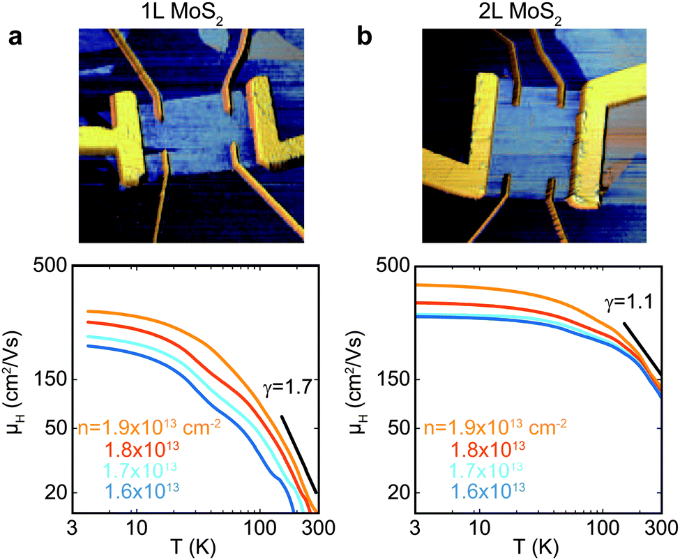 | ||
| Fig. 6 Dependence of Hall mobility (μH) on temperature for (a) monolayer and (b) bilayer MoS2 FETs after long-time thermal annealing at different carrier densities. Top panels are the color-enhanced AFM height images for the corresponding devices. Bottom panels are the mobility data and the power-law temperature fitting near room temperature. Reproduced with permission from ref. 172, copyright 2013, American Chemical Society. | ||
3.3 Dependence of the electronic phase on carrier density
The layered MX2 chalcogenides exhibit a rich phase diagram depending on carrier density (n2D) as a result of complicated electron–electron interaction. Fig. 7 shows the results on carrier density by Iwasa et al. who first investigated the electronic behavior of 20 nm thick MoS2 over a wide range of n2D through ionic liquid gating. With this, an extremely high n2D value up to 1014 cm−2 is reached such that the superconducting phase can be accessed. As shown in the phase diagram (Fig. 7b), the thick MoS2 flake exhibits a semiconducting (insulating) phase as n2D < 6.7 × 1012 cm−2, a metallic phase from 6.7 × 10¹² to 6.8 × 1013 cm−2, and a domelike superconducting phase as n2D > 6.8 × 1013 cm−2. The critical density for the insulator–metal transition n2D = 6.7 × 1012 cm−2 corresponds to a sheet resistance Rs = 21.7 kΩ per square (Fig. 7d), which is close to the quantum resistance h/e2 and is consistent with the metal–insulator transition found in other 2D systems.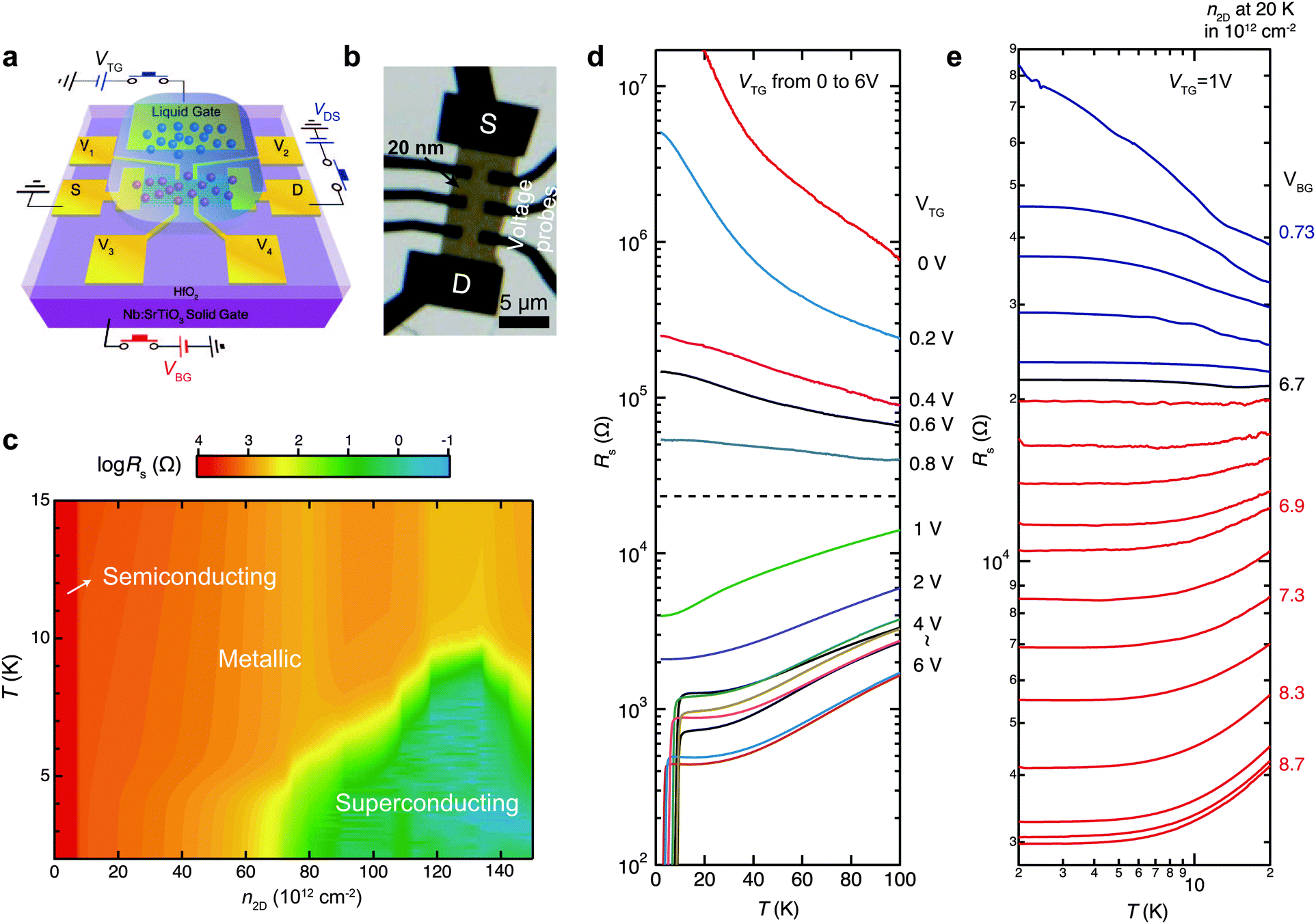 | ||
| Fig. 7 (a) Schematic and (b) optical images for an ionic liquid gated (TG) MoS2 FET. (c) Phase diagram showing the evolution of electronic phases as a function of carrier density n2D. (d) Temperature dependence of the channel sheet resistance Rs at different VTG gate biases ranging from 0 to 6 V (indicated on the right). (e) Temperature dependence of Rs at VTG = 1 V and different VBG showing a metal–insulator transition at n2D = 6.7 × 1012 cm−2. For each VBG, the corresponding n2D is determined by Hall measurement at 20 K. Reproduced with permission from ref. 224, copyright 2012, American Association for the Advancement of Science. | ||
The metal–insulator transition was soon confirmed in the monolayer MoS2 samples.82,172,173,222,225 However, the superconducting phase is absent,173,225 indicating the detrimental role played by the interfacial impurities that are strong enough to destroy the electrostatic surrounding required to form the superconducting cooper pairs.
The semiconducting regime with medium n2D is critical for FET applications. In this regime, the variation of carrier density has two opposite effects to the channel mobility. On the one hand, high n2D is beneficial for screening the interfacial impurity potential that increases mobility. On the other hand, high n2D also increases the carrier energy such that they are interacted with high-energy scattering centers, which may reduce mobility.131 Hence, there is normally an optimized carrier density for achieving the best carrier mobility.
In a very low n2D regime, some groups reported a hopping-like transport behavior,221,226,227 which was interpreted that most carriers are filled into the band tails where carriers are highly localized. Another possible explanation to this behavior is the presence of large contribution of the contact resistance, which becomes increasingly important at low temperature and produces the artificial behavior of ln![[thin space (1/6-em)]](https://www.rsc.org/images/entities/char_2009.gif) σ ∼ T−1/3 since most reports of hopping transport behavior are observed in two-terminal devices.221,222,226 No trace of hopping behavior was seen in the devices with a four-terminal measurement where the contact contribution is eliminated.82 Instead, only thermal activation behavior was observed in this regime.
σ ∼ T−1/3 since most reports of hopping transport behavior are observed in two-terminal devices.221,222,226 No trace of hopping behavior was seen in the devices with a four-terminal measurement where the contact contribution is eliminated.82 Instead, only thermal activation behavior was observed in this regime.
4 Factors related to electronic transport
The carrier mobility of bulk MX2 chalcogenides can reach ∼200 cm2 V−1 s−1 at room temperature.127 The last section showed that most 2D MX2 chalcogenides exhibit reduced mobility in comparison with their bulk phase. To develop technologically viable 2D semiconductors, especially for atomically-thin-body FETs, it is highly desired to unravel the origin of such adverse thickness dependence.It is well known that silicon shows thickness dependence below ∼4 nm with a power-law thickness scaling behavior (μ ∼ t−6),107,109 as a result of the inevitable compositional transition from the SiO2 dielectric to Si channel, i.e. the issue of surface roughness (SR). However, this factor can be confidently ruled out in case of 2D vdW semiconductors because of the atomically well-defined interlayer interfaces. Studies indicate that there are two aspects responsible for the thickness dependence in the 2D vdW semiconductor:228 (1) carrier injection at the electrode/channel contacts and (2) carrier scattering within the conduction channels from the interfacial Coulomb impurities.
4.1 Electrode/semiconductor contacts
Contact issue is ubiquitous at all metal/semiconductor interfaces due to the formation of interfacial Schottky barriers which blocks efficient carrier transfer. Fig. 8 shows related studies on the contact resistance for MoS2. Strictly speaking, the contact does not affect the intrinsic carrier mobility in semiconductors; this unfavorable effect can be ruled out by employing a transfer-line method or four-terminal measurement (Fig. 8a). However, the practical FETs collect current with two electrodes (source and drain). In most cases, the field-effect mobility μFE, defined as the derivative of drain current to gate bias, is used to evaluate the channel performance. Normally the contact resistance does not depend on gate bias as strongly as channel resistance, the presence of contact resistance thus leads to underestimation of semiconductor performance when adopting μFE as the evaluation criteria.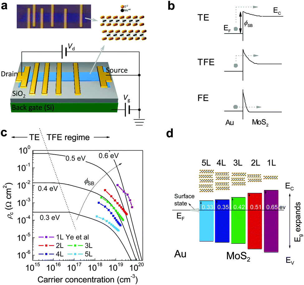 | ||
| Fig. 8 (a) Schematic diagram and real optical image for the geometry of transfer line measurement. The inset shows the atomic structure of MoS2. (b) Schematic band alignments between the Au electrode and channel MoS2 and the evolution of the three carrier injection mechanisms from low to extremely high carrier densities: thermal emission (TE), thermal field emission (TFE), and field emission (FE). The difference among the three injection mechanisms lies in the width of an interfacial barrier which changes with the carrier density in channels. (c) Comparison of the room temperature contact resistivity (solid dots) with theoretical calculation of TE and TFE conduction mechanisms to extract injection barrier height (ϕSB). (d) Evolution of energy level alignment at the Au/MoS2 interfaces as MoS2 thickness reduces from 5 to 1 layer. Adapted with permission from ref. 229, copyright 2014, American Chemical Society. | ||
However, the actual injection barrier height is also governed by the effect of Fermi level pinning due to the presence of interface states of semiconductors. The pinning effect is more pronounced when the channels become atomically thick because the density of interface states enhances considerably. The barrier height ϕSB is proportional to the potential difference of the energy levels Δu between semiconductors and electrodes, expressed as ϕSB = βΔu with β a coefficient between 0 and 1, representing the strong and weak pinning limits, respectively.230
It is widely accepted that the electrode/semiconductor contacts play a crucial role in the overall device performance. In early times, the variation of barrier width upon applying gate bias has ever been suggested as the current switching mechanism in FETs with nanostructured channels (e.g. carbon nanotube FETs).231 Transistors operated under this switching mechanism are termed as ‘Schottky barrier transistors’. At low carrier density the injection is dominated by a thermal emission process, while the injection becomes thermal-field emission (thermally assisted tunneling) or even field-emission (direct tunneling) at high carrier density, as shown in Fig. 8b.
Such a switching mechanism has also been proposed on monolayer MoS2 FETs where a faster variation is observed in contact resistance than channel resistance in the sub-linear conduction regime.232 It is found later, however, that the influence of contact resistance also depends highly on channel thickness and channel length. The contact may not dominate in FETs with a long channel length. In another report on mechanically exfoliated bilayer and hexalayer MoS2 samples, Chen et al. reported that the contact resistance comprises only 5–20% of the total channel resistance,179 indicating that the heights of contact barriers are smaller in thick flakes.
Furthermore, for the few-layer thick 2D semiconductors, the contact barrier height can be modified by the quantum confinement effect through the change in the semiconductor bandgap.233 To address this issue, Li et al. performed a systematic thickness scaling study on Au/2D MoS2 contacts using the transfer line method to extract the area normalized contact resistivity (ρc) for each MoS2 layer.229 For MoS2 thinner than 5 layers, the contact resistivity sharply increases with reducing MoS2 thickness, as a consequence of bandgap expansion (Fig. 8c). Fig. 8d plots a full evolution diagram of energy level alignment to elucidate the thickness scaling effect. The interfacial potential barrier is varied from 0.3 to 0.6 eV with merely reducing MoS2 thickness. The thickness-dependent barrier height for charge injection is one of the reasons responsible for the field-effect mobility degradation in the ultrathin flakes. Hence, optimizing the contact quality is crucial for improving the mobility of the two-terminal FETs with 2D semiconductor channels.
For 2D channels, the vertical current injection path at the electrode/channel interface and the lateral current distribution in the channels can be analytically solved via a resistor network model,234 in which the electrode/channel stack is divided into infinite resistor and conductor elements. Fig. 9a shows the schematic distribution of the impedance elements at the contact interface dG = ρc−1wdx and in the channel dR = Rsw−1dx, where Rs, ρc, w, and x denote the channel square resistivity, area contact resistivity, channel width, and channel coordinate, respectively. It has been derived that the lateral channel current i(x), vertical interface potential u(x), and vertical injection density j(x) satisfy the relations below234
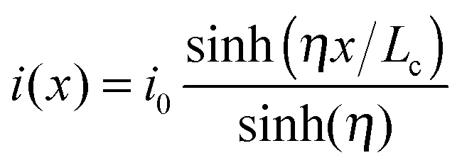 | (1) |
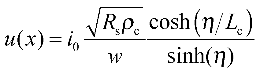 | (2) |
| j(x) = u(x)/ρc | (3) |
 is the transfer length, which is a characteristic length for current injection phenomena. In particular, Rc, Rs, and ρc are linked by
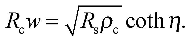 | (4) |
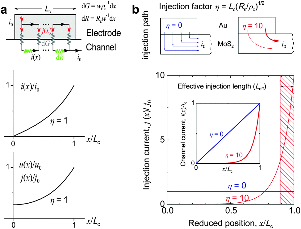 | ||
| Fig. 9 (a) Resistor network model for analysing the distributions of injection current along a probe/channel stack. Top: Current injection path and distribution of impedance elements at the probe/channel interface (modeled as dG) and in the channel (modeled as dR). Bottom: Plots of lateral channel current i(x), vertical interfacial potential u(x) and injection current density j(x) at η = 1. (b) Comparison of two extreme cases of η = 0 and 10. Reproduced with permission from ref. 229, copyright 2014, American Chemical Society. | ||
According to eqn (1)–(3), the carrier injection at contact is governed by the η factor which is a function of Lc, ρc, and Rs. Fig. 9a depicts an illustrative distribution of i(x), u(x), and j(x) at η = 1. Apparently, the injection is rather asymmetric along the x axis. To deepen our understanding, Fig. 9b plots two extreme cases for η = 0 and 10. As η = 0 (e.g. in the presence of a superconducting channel with Rs = 0 or a bad contact with ρc → ∞), the current is uniformly injected along the entire channel. At η = 10 (e.g. in case of a wide electrode with large Lc or small ρc), the crowding behavior is aggravated and half of the current is injected from ∼10% portion from the side. For typical MoS2 devices η is in the range of 2–5 depending on gate bias.
In device physics, one can use the transfer length  to estimate the minimum electrode length (few times of LT) that enables efficient current injection. For Ti contacted 1L MoS2, Ye et al. estimated LT is 1.26 μm at 0 V gate bias and drops to 0.63 μm at high gate biases.232 They suggested that the contact length should be at least 1 μm (1.5LT) to guarantee good contact at device on state. In contrast to the shrinking tendency with increasing gate bias, Chen et al. observed an LT behavior increasing with elevating gate bias in their few-layer samples.179 It increases from 20 to 80 nm for Ti/2L MoS2 contact, from 50 to 180 nm for Ti/6L MoS2, and from 30 to 200 nm for Au/6L MoS2. Independently, Li et al. extracted LT from 200–400 nm for thermally annealed Au contacted few-layer MoS2 (2–9L).229 It seems that the contact length depends highly on the semiconductor thickness and whether the samples have undergone annealing treatment. For most appropriate annealed devices, the contact length would not be a limit to MoS2 performance since most devices employ electrodes longer than 500 nm (limited by lithographic resolution).
4.2 Carrier scattering mechanisms
In this subsection, we give a fundamental introduction to the main scattering mechanisms in semiconductors, including Coulomb impurities, lattice phonons and remote interfacial phonons. Fig. 10 schematically depicts the carrier scattering processes where the orange balls and dashed arrows represent the carriers and their transport paths, respectively. The change in the direction of the carrier path results in a scattering event. The common method to calculate the scattering rates for each mechanism is to solve the Boltzmann transport equation within the relaxation-time approximation. To this end, one has to derive the scattering matrix elements M2D, electron polarization function for the 2D channels ε2D, and configurative form factor Φ(q,t) according to the device configuration. Here, we will summarize the main theoretical results and show the derived calculating formulae without dealing with the derivation. For detailed theoretical analyses, we recommend the readers to refer to related literature.235–238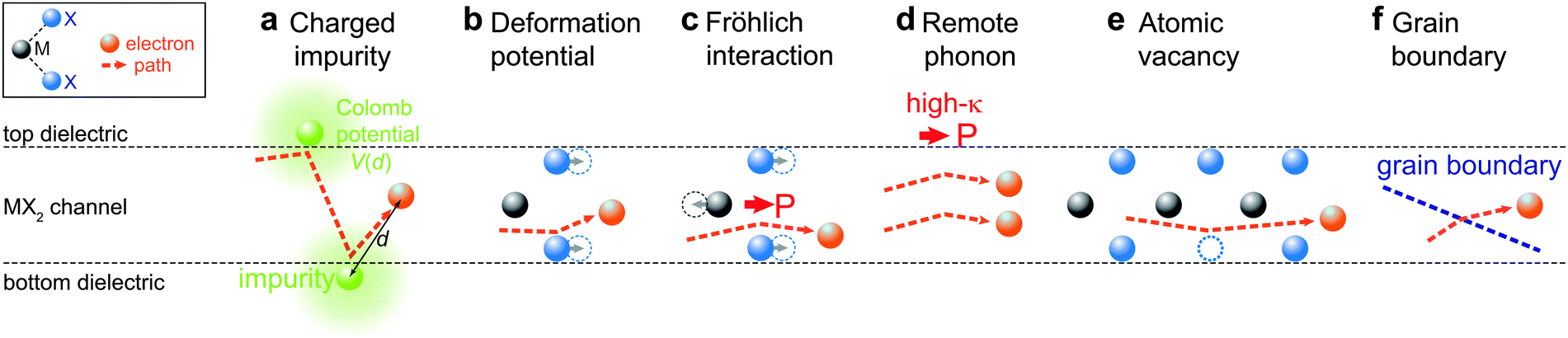 | ||
| Fig. 10 Schematic diagrams of leading carrier scattering mechanisms in 2D MX2 channels. The black and blue balls denote the M and X atoms, respectively. The orange balls and corresponding arrows denote the electrons and their paths in the channels. (a) Charged interfacial impurities at both the top and bottom channel surfaces. The green balls and the outer surroundings denote the impurities and corresponding scattering potential V(d). (b) Deformation potential of phonons due to atom vibration. (c) Fröhlich interaction due to polar optical phonons. The red arrow denotes the oscillating polar electric field induced by the polar optical phonon. (d) Remote interface phonon from dielectric. The red arrow denotes the polar phonon in the top dielectric. (e) Atomic vacancies (dashed circle) which tend to form in both natural and synthetic chalcogenides. (f) Grain boundaries (dashed line) which are typically present in synthetic chalcogenides. | ||
While the theoretical calculations on various symmetric systems (i.e. superlattices, graphene, and silicon FETs) have been performed, the calculation on a generalized asymmetric system remains invalid. As mentioned, the challenging parts are the derivations of the scattering matrix element M2D, configurative form factor Φ(q,t), and carrier polarization function ε2D according to the exact device configurative parameters (i.e., carrier distribution, symmetry of dielectric surroundings, and channel thickness). In most symmetric systems, the three terms can be analytically expressed,109,238–241 while they are only numerically solvable for complex systems.130
Fig. 11 depicts the difference for four device configurations. Here we use εi (i = 1, 2, 3) to denote the dielectric constants for different layers of channel and dielectrics. For superlattice with a periodic structure of two semiconductor layers (Fig. 11c), one often adopts a symmetric carrier distribution (trigonometric) and a symmetric dielectric environment (ε2 = ε3). For graphene (Fig. 11b), the thickness of the channel (0.35 nm) is negligible which enables the use of a pulse-like δ function to represent the carrier distribution. In general, the high symmetries exhibited enable analytic expression for the three factors of M2D, ε2D, and Φ(q,t). The situation is difficult in the case of silicon FETs (Fig. 11a) because it involves many configurative asymmetries. Upon adopting an empirical form of carrier distribution, analytic forms for the three items can still be reached.238 Nevertheless, none of the three device configurations is suitable for the generalized MoS2 FET since it possesses a finite channel thickness (non-negligible thickness), asymmetric dielectric environments (i.e., ε2 ≠ ε3), and lopsided carrier distribution (close to the gated dielectric). Compared to silicon, the MoS2 FET has one more top dielectric needed to be considered.
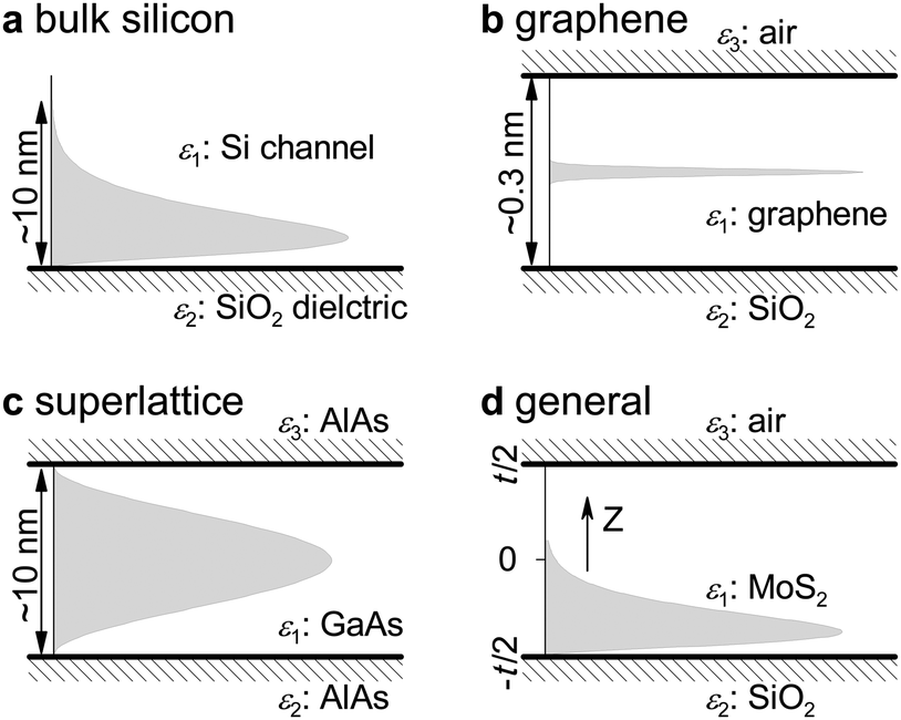 | ||
| Fig. 11 Schematic diagrams of dielectric environments and carrier distributions for different FET configurations. (a) Bulk silicon: one boundary which produces only one image charge.238 (b) Graphene: negligible thickness in the middle channel (t ∼ 0.3 nm) that enables the approximation of a simple pulse-like carrier distribution.239,240 (c) Superlattice: symmetric dielectrics and trigonometric carrier wavefunction.109,241 (d) A general FET with complicated device configuration: (1) two channel boundaries which can produce infinite image charges when considering charge–charge interaction; (2) a lopsided carrier distribution which leads to complicated configurative form factors Φ(q,t) in scattering matrix elements M2D and electron polarization function ε2D. Reproduced with permission from ref. 131, copyright 2013, American Chemical Society. | ||
Jena et al. are the first to calculate the scattering of charged impurities in 2D MoS2 FETs.130 They achieved the carrier distribution in multilayer MoS2 by numerically solving the Schrödinger–Poisson equation. Such a treatment, albeit accurate, requires a case-by-case calculation for each channel thickness or gate bias because any variation in them would change the carrier distribution. Later on, they did an analogue simplification to graphene in calculating the monolayer MoS2 by adopting zero channel thickness and symmetric carrier distribution.132
To combine accuracy and convenience, Li et al. employed a phenomenological method by adopting the carrier distribution from silicon FETs.131 In their calculation they strictly considered the configurative parameters of devices, including non-zero channel thickness, asymmetric surroundings, and positions of interfacial impurities. This method allowed them, for the first time, to shed light on the dependence of mobility over the full range thickness. In their calculation, the impurity scattering rate can be expressed as a linear combination of the contributions from the top and bottom channel surfaces as
| τCI−1 = αbot(t)nbot + αtop(t)ntop | (5) |
Two major pieces of information can be understood. First, the impurity scattering from the interface of gated dielectric is stronger than the ungated interface as a result of lopsidedness of carrier distribution upon applying gate bias. For the monolayer MoS2, the scattering from charged impurity would outperform that from phonons if the gated interface had impurity density higher than ∼2 × 1012 cm−1. Second, the impurity scattering is considerably enhanced in extremely thinned channels, resulting from the reduction of interaction distance (dNL) between impurities and carriers. As an example, Fig. 12c shows the carrier distribution and the interaction distance d1L and d3L for the back-gated 1L and 3L FET channels, respectively. The carriers in the thinner 1L channel are located closer to the gated bottom dielectric due to electrostatic equilibrium, resulting in a smaller d1L than d3L. Since scattering potential V(d) ∝ d−1, the scattering intensity on the thin channels is stronger than on the thick ones. Therefore, the variation of interaction distance with channel thickness is the direct origin for the dependence of carrier mobility on thickness.131Fig. 12d compares the experiment and calculation of the mobility values at different thicknesses. Reasonable agreement is reached in terms of the thickness dependence.
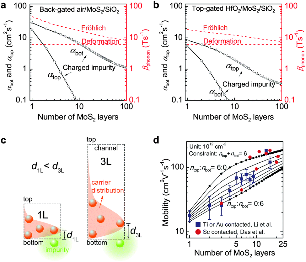 | ||
| Fig. 12 (a and b) Calculated Coulomb impurity scattering coefficients at the top and bottom channel surfaces (αtop and αbot) for different channel thicknesses. For comparison, the scattering rates of phonon deformation and Fröhlich interaction (βphonon) are also plotted on the right longitudinal axis in red. (a) is for back-gated air/MoS2/SiO2 and (b) for top-gated HfO2/MoS2/SiO2 FETs. (c) Schematic diagram of the origin of dependence of impurity scattering intensity on channel thickness. The underlying nature is the variation of interaction distance (dNL) between the impurities and the channel carriers as channel thickness changes. For instance, for the 1L and 3L MoS2 samples d3L > d1L and hence the scattering rate is lower in the 3L sample (i.e., carrier mobility is higher). (d) Comparison between the experiment and calculation based on impurity and phonon scattering. Reproduced with permission from ref. 131, copyright 2013, American Chemical Society. | ||
Based on the above results, a general conclusion can be drawn that it is crucial to achieve clean channel interfaces in order to realize high mobility in extremely thinner 2D semiconductors. Specific strategies will be discussed in Section 5.2.
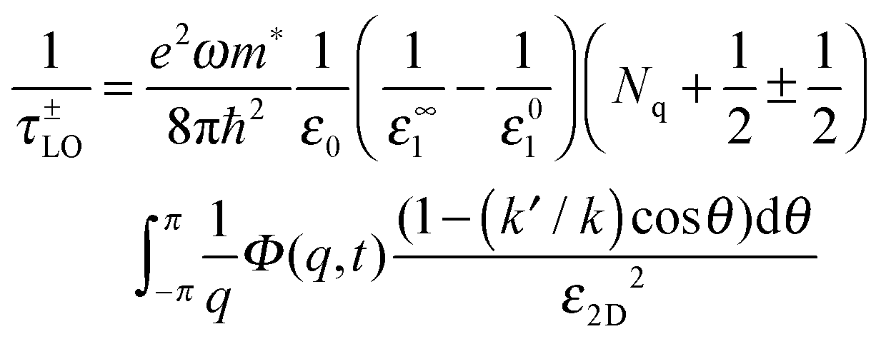
Phonon scattering depends highly on temperature because the number of phonons follows the Bose–Einstein distribution Nq = 1/[exp(ℏω/kBT) − 1], where ℏω is the phonon energy. The expressions of phonon scattering rates and related physical parameters for the monolayer MoS2 have been derived by Kaasbjerg et al.128,129Table 4 summarizes the phonon parameters required in the calculation. To account for the screening effect, Jena et al. included the electron polarization function ε2D in the calculation. Hence the scattering rate due to the deformation potential of the acoustic phonon is written as132
 | (6) |
 | (7) |
 | (8) |
 | (9) |
] is the step function, Ek is the carrier energy at momentum k, ω is the phonon frequency, and q = 2k·sin(θ/2) is the scattering vector. The superscript + and − represent scattering processes with absorbing and releasing a phonon, respectively. The subscript ν = 0 and 1 denoting the zeroth- and first-order optical deformation potential, respectively.
| Parameter | Symbol | Value |
|---|---|---|
| Lattice constant | a | 3.14 Å |
| Ion mass density | ρ | 3.1 × 10⁻⁷ g cm−2 |
| Effective electron mass | m* | 0.48 me |
| Valley degeneracy | g v | 2 |
| Effective layer thickness | σ | 5.41 Å |
| Piezoelectric constant | e 11 | 3.0 × 10⁻¹¹ C m−1 |
| Transverse sound velocity | c TA | 4.2 × 10³ m s−1 |
| Longitudinal sound velocity | c LA | 6.7 × 10³ m s−1 |
| Acoustic deformation potentials | ||
| TA | Ξ TA | 1.5 eV |
| LA | Ξ LA | 2.4 eV |
| Optical deformation potentials | ||
| TA | D 1 K,TA | 5.9 eV |
| LA | D 1 K,LA | 3.9 eV |
| TO | D 1 Γ,TO | 4.0 eV |
| TO | D 1 K,TO | 1.9 eV |
| LO | D 0 K,LO | 2.6 × 10⁸ eV cm−1 |
| Homopolar | D 0 Γ,HP | 4.1 × 10⁸ eV cm−1 |
| Phonon energies | ||
| TA | ℏω K,TA | 23 meV |
| LA | ℏω K,LA | 29 meV |
| TO | ℏω Γ,TO | 48 meV |
| ℏω K,TO | 47 meV | |
| LO | ℏω Γ,LO | 48 meV |
| ℏω K,LO | 41 meV | |
| Homopolar | ℏω HP | 50 meV |
The scattering rate for Fröhlich interaction is given by132,242
 | (10) |
Kaasbjerg et al. derived the scattering matrix element for the piezoelectric interaction in 2D MoS2,129
| |MqλPE| = e11eq/ε0 × erfc(qσ/2)|Aλ(q)| | (11) |
) is the complementary error function, σ is an effective width of the electron wave functions, and Aλ(q) is the anisotropy factor that accounts for the anisotropic angular dependence of the piezoelectric interaction. Within the long-wavelength approximation, the high-temperature relaxation time for piezoelectric scattering can be calculated together with the acoustic phonon scattering as129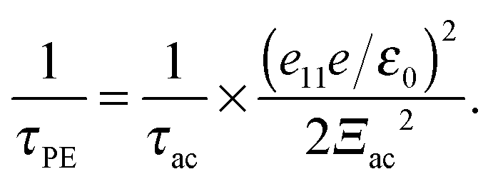 | (12) |
| Dielectric | ε 0ox | ε ∞ox | ω 1RIP | ω 2RIP |
|---|---|---|---|---|
| SiO2 | 3.9 | 2.5 | 55.6 | 138 |
| BN | 5.1 | 4.1 | 93.1 | 179 |
| AlN | 9.1 | 4.8 | 81.4 | 88.5 |
| Al2O3 | 12.5 | 3.2 | 48.2 | 71.4 |
| HfO2 | 22 | 5.0 | 12.4 | 48.4 |
| ZrO2 | 24 | 4.0 | 16.7 | 57.7 |
On the assumptions of zero thickness for 2D channels and semi-infinite for dielectrics, the electron-RIP coupling parameter is
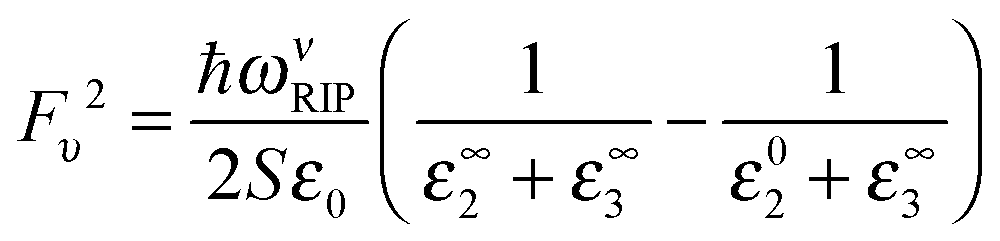 | (13) |
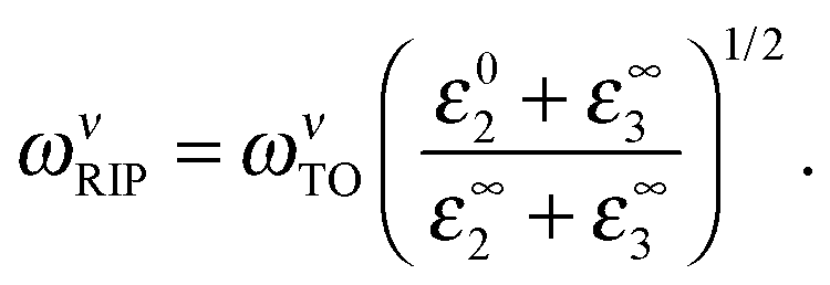 | (14) |
 | (15) |
The significant room-temperature RIP scattering rate for high-κ dielectric in monolayer MoS2 FETs poses a challenge to the dielectric screening engineering advocated,81,241 which is oriented to enhance carrier mobility. We will elaborate this issue in Section 5.3.
The defect scattering is normally not considered in high-quality superlattices and silicon FETs,238 because the very low density causes negligible scattering rates relative to other mechanisms. However, the defect density is by no means low in the 2D vdW crystals. Fig. 13 shows the structures and corresponding formation energies of different atomic defects in MoS2. The sulfur vacancies have a rather low formation energy of ∼1.6 eV, hence the anion vacancies tend to form in chalcogenides, just like in oxides (e.g. ZnO), which is presumably a strong scattering source when the sample quality is not sufficiently high.
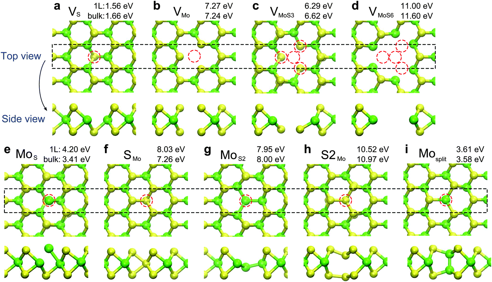 | ||
| Fig. 13 Optimized atomic structures and formation energies for different defects in the MoS2 monolayer (1L) and bulk. (a)–(d) Vacancies, (e)–(h) antisites, and (i) Mo–Mo split interstitial defect. Dashed circles (red) denote the position of the defect. Owing to a rather low formation energy of ∼1.6 eV, sulfur vacancies tend to form in MoS2. Reproduced with permission from ref. 269, copyright 2015, American Physical Society. | ||
High-resolution TEM experiments revealed the presence of large amounts of point defects and grain boundaries in natural and synthesized MoS2.227,262,270,271 It is found that the structures of dominant defects correlate closely with material growth methods. For samples prepared by mechanical exfoliation and chemical vapor deposition (CVD), sulfur vacancy defects with one (denoted as VS, Fig. 13a) or two (VS2) S atoms absent are frequently observed, while the dominant defects for the physical vapor deposited (PVD) samples are antisite defects with one Mo atom replacing one (MoS, Fig. 13e) or two (MoS2, Fig. 13g) S atoms.271 The density of sulfur vacancy can reach (1.2 ± 0.4) × 1013 cm−2 in exfoliated and CVD samples, corresponding to a surprisingly high atomic percentages of 0.4%. Undoubtedly, atomic defects would play an important role in carrier scattering, if such high-level defects are present in device channels.
Wang et al. attributed the presence of sulfur vacancies as the reason for the hopping transport behavior observed in the low carrier density regime.227 The short-range vacancy scattering is also proposed as one of the scattering mechanisms in the CVD MoS2 flakes by Eda et al.225 With long-time in situ thermal annealing to minimize contact resistance, they estimated a high extrinsic room-temperature mobility of 45 cm2 V−1 s−1 and an intrinsic mobility of 58 cm2 V−1 s−1 after deducting the effect of short-range vacancy scattering. Since the anion vacancies could be the leading scattering centers, vacancy repair is expected to improve device performance.
Hitherto, there has been no theoretical work on the vacancy scattering in 2D vdW semiconductors. However, one can quickly grasp their basic characteristics by looking through previous studies on their bulk272,273 and 2D analogue graphene.274,275 Unlike Coulomb impurity scattering, vacancy scattering is a kind of short-range interaction with the interaction range comparable to the lattice spacing (Fig. 10e). In this case, the scattering potential can be treated as a δ function.275 The scattering matrix in the low-energy regime becomes dispersionless on energy for 2D semiconductors because the Fourier transformation of the real space δ potential is a constant in the reciprocal momentum space, which results in a constant scattering matrix. Hence, the scattering rate of atomic vacancies is independent on carrier density, manifested itself as a resistivity background as in graphene.274 In addition the vacancy scattering in 2D systems should be weakly dependent on temperature or channel thickness because the defect density is independent on these two parameters. It would reduce the temperature dependence of mobility and the temperature exponent γ, once vacancy scattering becomes important. In this sense, the low γ values (∼0.7) observed in clean samples221,222 is likely indicative of the emergent dominance of vacancy scattering. Overall, it is expected that defect scattering would become paramount in very clean samples or at low temperature when Coulomb impurity and phonon scattering rates are low.223
Grain boundary is another typical form of defect commonly present in synthesized samples. Fig. 14a–f show two types of grain boundaries (the mirror and title type), as seen by optical microscopy and photoluminescent mapping.270,276,277 An important question for device applications is whether these grain boundaries disrupt or modify electronic transport. Hone et al. compared the electronic transport properties of exfoliated and synthesized MoS2 flakes with room temperature mobilities from 1 to 8 cm2 V−1 s−1.270 They found that device performance strongly depends on the boundary type as well as current flow direction. The mirror twin boundary has little effect on channel conductivity when current is perpendicular to boundary and, surprisingly, it slightly increases the on-state conductivity when current flows in parallel (Fig. 14g). This observation suggests that the few-atom-wide twin boundaries, although still semiconducting, have similar conductivity of pristine MoS2. In contrast, the tilt boundary generally degrades the device performances to a large extent in any current direction (Fig. 14h). A wide variation of the conductance (5–80%) is observed among devices, implying a complicated dependence of the electronic structure at boundaries on the tilt angle and the atomic structure.278
 | ||
| Fig. 14 Optical and electronic properties of mirror and tilt boundaries in synthesized MoS2 flakes. (a–c) Optical measurements of a MoS2 flake containing a mirror twin boundary. (d–f) Corresponding measurements of a MoS2 flake containing a tilt boundary. Panels (a) and (d) are optical images; panels (b), (c), (e) and (f) are colour plots of photoluminescence. Panels (g) and (h) show the transfer curves of four FETs fabricated from the MoS2 flakes with mirror and tilt boundaries in the insets. Reproduced with permission from ref. 270, copyright 2013, Nature Publishing Group. | ||
5 Mobility engineering strategies and state-of-the-art performance
5.1 Contact optimization
It is well known that the presence of contact resistance strongly limits the current carrying capacity in FETs. The contact resistance for 2D chalcogenides ranges from 10–100 kΩ μm at Au/MoS2 contacts229 to ∼1 kΩ μm at graphene/2L WSe2 contacts.214 These values are at least 1–2 orders higher than the requirement of the deep-nanometer technological node in the semiconductor industry. Hence, optimizing the electrode/channel contacts is highly desired.Fig. 15 summarizes the mobility engineering strategies devised for contact optimization. Thermal annealing is traditionally used to reduce contact resistance. This technique is particularly necessary and effective for 2D chalcogenide FETs. Jarillo-Herrero et al. found that a large contact resistance is the main reason for the low field-effect mobility in thermally untreated 2D FETs.172 A huge drop in contact resistance, with 2 orders of magnitude in monolayer and more than 1 order of magnitude in bilayer MoS2 devices, was observed after long-time (12 h), low-temperature (120 °C) in situ thermal annealing (Fig. 15b). Remarkably high room temperature mobility values of 20–50 and 80–150 cm2 V−1 s−1 were observed in monolayer and bilayer MoS2, respectively. In their experiment, low annealing temperature was used likely because of the safety limitation of test cables and cryostat, which, however, favorably prevents the decomposition of MoS2 during annealing and the creation of sulfur vacancies, a kind of short-range carrier scattering center. The similar behavior has been observed in CVD MoS2 samples by Eda et al.225 and 1L WS2 samples by Kis et al.208 (Fig. 15a). Fig. 15c shows the real-time monitor of the mobility evolution with annealing time for the 1L WS2 sample under both two-terminal and four-terminal measurements. After a long annealing time of 150 h, the mobility extracted by the four-terminal method remains 2-fold higher than that extracted by the two-terminal method, suggesting that the contact issue, though largely reduced, cannot be completely eliminated by thermal annealing.
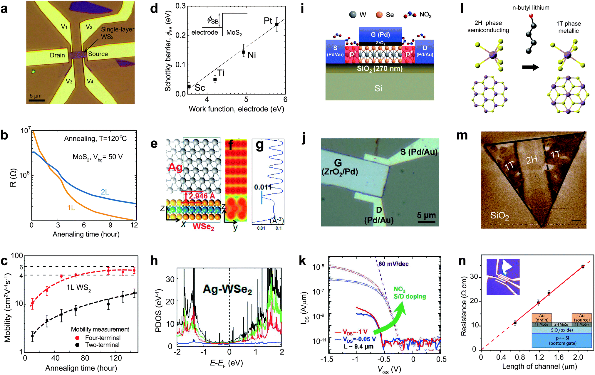 | ||
| Fig. 15 Mobility engineering for contact optimization. (a–c) Thermal annealing. (a) Optical image of 1L WS2 four-terminal measurement geometry which can be used to estimate the contact quality. (b) Evolution of contact resistance at the Ti/MoS2 interface under low-temperature (120 °C) and long-time thermal annealing up to 12 h. (c) Mobility comparison for 1L WS2 under different wiring methods (two-terminal and four-terminal), showing that the contact resistance is difficult to be eliminated since the difference of mobility values under the two wiring methods exists all the time (up to 150 h annealing). (d) Energy level matching, which shows that electrodes with low work functions in general lead to low contact barrier to n-type semiconductors. Adapted with permission from ref. 181, copyright 2013, American Chemical Society. (e–h) Orbit hybridizing engineering. (e) Side view of the relaxed contact regions at the WS2/Ag(111) interface. (f and g) Show the contour plot of the spatial electron density and the average line electron density, respectively. (h) Partial density of states (PDOS) of the Ag–WS2 system. Hybridization states occur at the contacts which are beneficial for carrier transfer. (i–k) Contact doping engineering. (i) Schematic diagram for using NO2 gas to dope the channel edges in vicinity of contacts. (j) Optical device image with top ZrO2/Pd gate stacks. (k) Comparison of channel current before and after NO2 doping. (l–n) Phase change engineering. (l) Atomic phase change of MoS2 from 2H to 1T structure after soaking in n-butyl lithium. (m) Electrostatic force microscopy phase image of a 1L MoS2 nanosheet showing the difference between locally patterned 2H (bright colour) and 1T (dark colour) phases. The scale bar is 1 μm. (n) Transfer line plot for the 1T phase contacted MoS2 channels. The intercept is close to zero, indicating the contact resistance is very small. Panels (a) and (c) are reproduced with permission from ref. 208, copyright 2014, American Chemical Society. Panel (b) is reproduced with permission from ref. 172, copyright 2013, American Chemical Society. Panels (e)–(h) are reproduced with permission from ref. 279, copyright 2013, American Chemical Society. Panels (i)–(k) are reproduced with permission from ref. 280, copyright 2012, American Chemical Society. Panels (l)–(n) are reproduced with permission from ref. 137, copyright 2014, Nature Publishing Group. | ||
Energy level matching between electrodes and semiconductors was also employed to improve the field-effect mobility. The height of the contact barrier is highly related to the work function of metal electrodes, as shown in the inset of Fig. 15d. The metal Sc, with a low work function of 3.5 eV which is close to the electron affinity of MoS2 ∼4.0 eV, is found to form an electrically transparent interface with thick MoS2.181 The mobility reaches 180 cm2 V−1 s−1 in ∼10 nm MoS2 devices. The pinning coefficient is estimated to be 0.1, as compared with ∼0.3 in bulk silicon, suggesting the presence of an extremely strong pining effect in 2D semiconductors due to the full exposure of channel surfaces. Nevertheless, the energy level matching with the Sc electrode seems an effective way to improve mobility for thick channels but to be much less influential for ultrathin samples. The carrier mobility was found to sharply drop to 25 cm2 V−1 s−1 in ∼2 nm MoS2, indicating a more complicated behavior in the ultrathin regime. This can be ascribed to the expansions of the bandgap and hence the contact barrier due to quantum confinement (Fig. 8d). Owing to the upshift of the conduction band in the few-layer MoS2, electrodes with lower work functions are required to match the high-lying conduction band.
Graphene is also explored as a contact material to chalcogenides because it is a unique Dirac metal whose work function can be broadly tuned upon applying gate voltage.216,223,281,282 In particular, graphene contacted MoS2 shows extremely high low-temperature mobility when encapsulated by clean BN.223,282 The devices with graphene contacts will be discussed in Section 5.5.
Besides the empirical strategy, band structure calculation is also used to understand the interface physics to facilitate contact design between the metal and monolayer WSe2 (Fig. 8e–g). Calculations based on ab initio density functional theory (DFT) indicate that using d-orbital electron abundant transition metals as contacts like Ag and Ti are beneficial to form better electron injection into WSe2 because the d-orbitals in these metals can hybridize with the d-orbitals in the Se and W atoms (Fig. 8h).279 A considerably high carrier mobility of 142 cm2 V−1 s−1 is measured in thermally annealed Ag contacted monolayer WSe2 samples in a vacuum environment.
Apart from the rational choice of contact metals, contact doping by gas molecules or alkali metals is also developed as a chemical strategy to optimize contact quality.183,280 By introducing highly active electron donor NO2 to form heavily doped contact areas (Fig. 15i), Javey et al. observed a high mobility of 250 cm2 V−1 s−1 in top ZrO2 gated, Pd contacted p-type monolayer WSe2 FETs (Fig. 15j).280 They carefully compared the device current before and after NO2 doping and about 3 orders of magnitude enhancement in device current was observed (Fig. 15k), indicating the critical role of contact in achieving high device performance. Additionally, they observed a high mobility of >110 cm2 V−1 s−1 in a potassium doped 3L WSe2 FET.183
For the same reason, ionic liquid gating is used for contact engineering.215,216 This is because the injection of charges is assisted by high carrier density in channels near the metal/semiconductor contacts, which largely decreases the width of the injection barrier. As a result, carrier injection from the source/drain contacts is controlled by tunneling instead of by the over-the-barrier thermal activation process (Fig. 8b). Zhou et al. reported a high electron and hole mobility of ∼200 cm2 V−1 s−1 at 160 K and at ∼300 cm2 V−1 s−1 at 77 K in 6 nm WSe2.216 Similarly, Jarillo-Herrero et al. achieved a low contact resistance of <330 Ω μm and a high mobility of ∼600 cm2 V−1 s−1 at 220 K in 3L WSe2.215
Artificial engineered phase change has also been developed to increase contact quality.136–138 For chalcogenides, different atomic structures and phases may exhibit distinct electronic properties. Typically, the 2H phase of MoS2 is metallic while the 1T phase is semiconducting. After replacing the 2H phase with the 1T phase, Chhowalla et al. observed a ∼5-fold decrease of contact resistance from 1.1 to 0.2 kΩ μm at zero gate bias,137 a value comparable to the source/drain parasitic resistance in silicon FETs (290 Ω μm and 405 Ω μm for planar and SOI CMOS, respectively). As a result, the carrier mobility increases from 19 to 46 cm2 V−1 s−1. Direct doping and metallization at contacts is a promising way to achieve technologically viable 2D FETs.
5.2 Reduction of impurity scattering
Before discussing the technical routes, we first remark on the origin of the Coulomb impurities and corresponding experimental evidence, which may help to understand the nature behind. Fig. 16a schematically displays the sources of Coulomb impurities at the both interfaces of the FET channels, including gaseous adsorbates (e.g. humidity and oxygen molecules), unsaturated chemical bonds/groups at the dielectric surface, and chemical residues during device fabrication. It has been pointed out that the device current is higher in a vacuum than in an ambient measurement environment (Fig. 16b).180,221 The gaseous adsorbate such as humidity and oxygen molecules169,180,283 which results in charge transfer to the channel are believed to be an important Coulomb impurity source. The second impurity source can be attributed to chemical residues introduced during device fabrication, as evidenced by the increase in channel current in both exfoliated and CVD devices after performing long-time thermal annealing under ultrahigh vacuum.172,225 The dangling bonds, hydroxyl groups and charged ions in the surface of dielectric284 are believed to be the third type of impurity source since a remarkable current increase is observed in suspended MoS2 channels by etching out the underlying SiO2 dielectric (Fig. 16c).177,178,192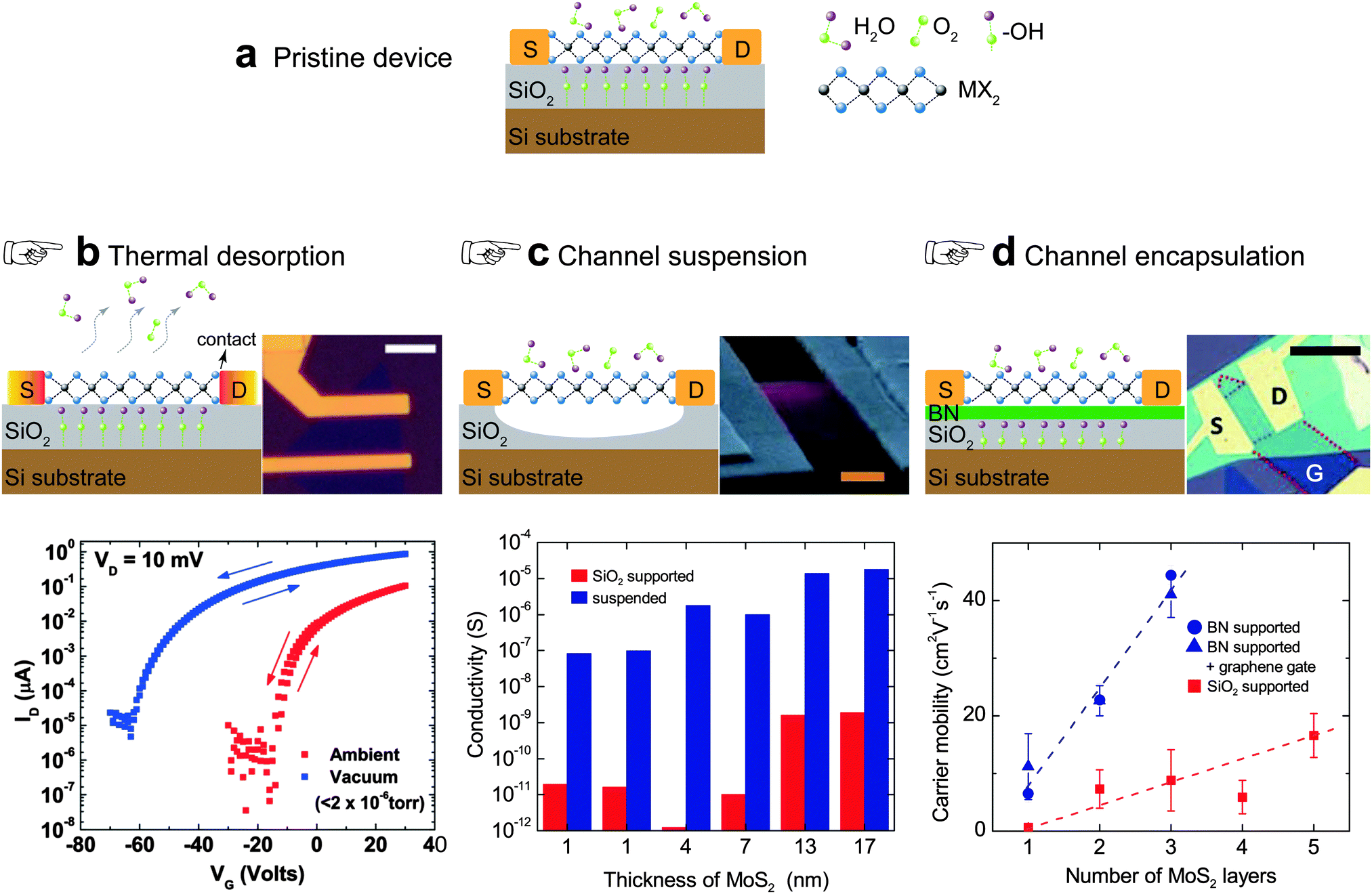 | ||
| Fig. 16 Mobility engineering for interfacial impurity suppression. (a) Schematic diagram of a pristine SiO2 back-gated FET consisting of a 2D MX2 channel. The main Coulomb impurities arise from the molecular absorbates on the top channel surface and the dangling bonds and the hydroxyl group (–OH) on the bottom channel surface (i.e. channel/dielectric interface). Three techniques are developed to suppress the impurity sources: (b) thermal desorption at ultrahigh vacuum, (c) channel suspension to remove the bottom impurities, and (d) channel encapsulation by clean dielectrics such as boron nitride or polymers (e.g. PMMA). In each panel from (b) to (d), the schematic techniques, typical device images, and corresponding effects on performance are illustrated. Panel (b) is reproduced with permission from ref. 221, copyright 2013, American Institute of Physics. Panel (c) is reproduced with permission from ref. 192, copyright 2015, Institute of Physics, UK. Panel (d) is reproduced with permission from ref. 175, copyright 2013, American Chemical Society. | ||
Fig. 16b–d show the main three schemes developed to suppress the Coulomb impurity sources including (1) thermal desorption at ultrahigh vacuum (Fig. 16b), (2) channel suspension to remove the bottom impurities (Fig. 16c), and (3) channel encapsulation by clean dielectrics such as the vdW dielectric hexagonal boron nitride (hBN) and hydrophobic polymers (e.g. PMMA) (Fig. 16d, only encapsulation at the bottom side is shown).
Thermal desorption is proven to be one of the most effective methods to improve mobility in chalcogenide. In the high vacuum measurement (2 × 10⁻⁶ Torr), Hersam et al. observed the highest room-temperature mobility of 60–70 cm2 V−1 s−1 for pristine (neither encapsulated nor suspended), two-terminal (mobility underestimation due to contact resistance) 1L MoS2,221 demonstrating that the gaseous adsorbates are one of the leading scattering centers. Here, it deserves to note the different roles played by the annealing surroundings. Annealing ex situ can only influence the contact quality while in situ vacuum annealing can further remove gaseous adsorbates. In addition, an ultrahigh vacuum and long-time treatment is particularly critical to complete the adsorbate desorption.172,208
Among the three schemes to suppress interfacial impurities, the first and third are technologically viable but the second one is only of scientific interest since a suspended channel would cause severe issues in mechanical stability. Besides, the channel suspension scheme on 2D chalcogenides seems not as successful as graphene. Naively, one expects suspended devices to have higher mobility, due to the removal of substrates that introduce trapped charges and other scattering centers. However, the electronic performance of most suspended 1L MX2 flakes fabricated to date remains much lower than SiO2 supported samples.177,178,192 One possible explanation is the higher chemical activity of MX2 chalcogenides than graphene in the substrate etchant which produces new scattering sites on channels after dielectric etching treatment.192 Additionally, the general worse contact in chalcogenide devices could be another factor in limiting the performance of suspended MX2 flakes. Recently, Lau et al. investigated the effect of thermal annealing conditions on the suspended MoS2 samples and they showed remarkable increase in mobility from 46 to 105 cm2 V−1 s−1 for a 17 nm thick sample.192
Channel encapsulation is always a challenging task due to either the incompatibility of encapsulation materials to processing (e.g. PMMA) or the complexity in fabrication (e.g. hBN). Nonetheless, interface engineering via channel encapsulation has been applied to fabricate high-performance MoS2 FETs. By placing multiple MoS2 flakes on PMMA dielectric and using four-terminal measurements, Fuhrer et al. demonstrated a high mobility value of ∼500 cm2 V−1 s−1 in ∼50 nm MoS2.285 With a similar dielectric material, Hu et al. observed a room-temperature mobility of 1055 cm2 V−1 s−1 in back-gated multilayer InSe,286 being an extremely high value comparable to silicon.
The atomically flat vdW dielectric hBN, which is free of dangling bonds and thus is in principle free of trapped charges, has proven to be beneficial for graphene electronics.287–289 It is naturally introduced into the chalcogenide devices. Kim et al. first adopted hBN as a dielectric layer in MoS2 FETs.175 An order of magnitude enhancement in field-effect mobility, from 0.5 to 7.6 cm2 V−1 s−1, is observed in the hBN supported monolayer MoS2 FETs, as compared with the conventional SiO2 supported devices. A high mobility of ∼45 cm2 V−1 s−1 is measured in a trilayer device. By comparing the mobility trend versus channel thickness, the authors pointed out that there is likely a remarkable contribution from the electrode/channel contacts that limit the mobility because contact resistance decreases with increasing channel thickness. Independently, Tsukagoshi et al. also fabricated hBN supported MoS2 FETs and observed similar behavior of mobility enhancement and thickness dependence.176 Moreover, they studied the temperature dependence and revealed that the clean hBN dielectric can suppress the carrier traps at the channel/dielectric interface, which converts the carrier transport in the monolayer MoS2 from hopping to the thermal activation mode. Besides MoS2, other MX2 chalcogenides were also explored. The mobility enhancement from 17 to 80 cm2 V−1 s−1 is observed in 4L WS2 after replacing the underlying dielectric from SiO2 to clean hBN.210
5.3 Dielectric screening versus RIP scattering
Since Coulomb impurity is one of the main scattering mechanisms in FETs, a dielectric engineering, i.e., employing high κ dielectrics, was proposed to be a strategy to reduce the Coulomb impurity scattering to carriers for the reason that the elevated permittivity of dielectrics is expected to enhance the screening ability to the adverse scattering potentials from internal and external Coulomb impurities.241 This strategy would be justifiable, if the adopted high κ dielectrics do not bring remote interfacial phonons, and appears working on 2D chalcogenides with low initial mobility. A noticeable performance enhancement was observed in monolayer MoS2 and SnS2 flakes,81,218 with carrier mobility increasing from few to ∼50 cm2 V−1 s−1.In fact, there is a growing controversy on the exact role of the dielectric environment in suppressing carrier scattering. Early on, it was found that high-κ dielectrics lead to low carrier mobility in FETs made of silicon and organic materials because of the carrier scattering of polar phonon at the channel/dielectric interfaces.243–247 In high-quality graphene, Geim et al. also pointed out that screening of Coulomb impurities by high-κ dielectrics has little effect on mobility.290 The same is also true in chalcogenides. Several groups confirmed that the introduction of high-κ dielectrics deteriorates, rather than improving, the mobility of high-quality chalcogenide devices.137,216 In MoS2 FETs with high initial mobility, Liao et al. recently observed a mobility degradation of 30–50% in top HfO2 gated MoS2, as compared with back SiO2 gated devices.291 Conversely, when dielectrics without available RIP modes are used such as polymer parylene, 2–3 fold enhancement in mobility, from ∼50 to 100–150 cm2 V−1 s−1, was observed in 10 nm MoSe2 samples.202 All the experimental observations can be well explained by taking into account the adverse RIP scattering accompanied by the use of high-κ dielectrics. Ma and Jena found that a FET can gain additional mobility enhancement from dielectric screening when the average permittivity of the top and bottom dielectrics is smaller than a critical value of 10.132 The adverse RIP scattering would outperform and degrade mobility once the average permittivity is higher than the critical value.
In this sense, the early observation of mobility enhancement after high-κ dielectric deposition in devices with low initial mobility is likely due to the facts mentioned below: (1) improvement of device contact by thermal annealing during the time-consuming atomic layer deposition (ALD) process for high κ dielectrics; (2) reaction and cleaning effect on the surface gaseous adsorbates (humidity and oxygen, which are one of the main Coulomb impurity sources) with the ALD precursors; and (3) encapsulation of the conduction channels and consequent insulation from external surroundings.
5.4 Atomic vacancy healing
Apart from the long-range charged impurities, short-range scattering factors such as anion vacancy in chalcogenides is also likely one of the leading carrier scattering mechanisms. Hence, it is desired to repair them with a chemical approach based on interface and molecular engineering when contact optimization and impurity scattering are already well addressed.Fig. 17 show a typical vacancy healing scheme assisted by interface engineering on dielectric and/or semiconductor with designed functional molecules. Due to the full exposure of sulfur planes, a post molecular surface modification and healing becomes realistic. By introducing a long-chain molecule with a chemical group at one end attaching to SiO2 and the other end modifying the MoS2 channel, one can form a self-assembly monolayer (SAM) at the surface of ‘dirty’ SiO2 dielectric (Fig. 17a). Lou et al. intentionally modified the chemical surroundings of the conduction channels in FETs with a series of designed SAMs.196 The higher mobility of ∼18 cm2 V−1 s−1 was observed in the thiol group (–SH) contacted MoS2 channels than those contacted by other groups of –OH, –SiO2, –CF3, –CH3 and –NH2 (Fig. 17b), due partially to the vacancy repair effect. They concluded that the mobility improvement is a combined effect of interface-related effects of charge transfer, built-in molecular polarities, varied densities of defects, and remote interfacial phonons.
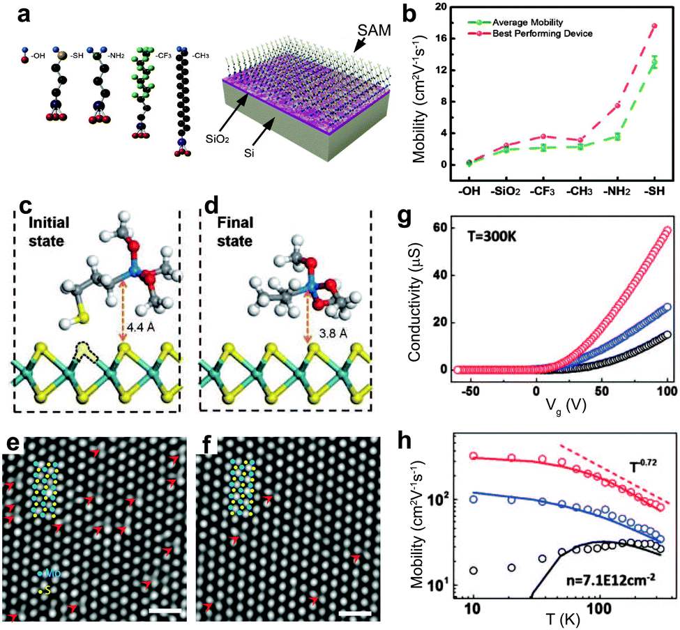 | ||
| Fig. 17 Mobility engineering for atomic vacancy healing. (a) Schematic molecules which can form a self-assembly monolayer (SAM) onto SiO2 substrates. (b) Comparison on the MoS2 mobility modified by different surficial chemical groups present at the SiO2 dielectric after SAM modification. Panels (a and b) are reproduced with permission from ref. 196, copyright 2014, American Chemical Society. (c and d) Calculated molecular reaction and layout before and after sulfur vacancy healing. (e) and (f) Corresponding high-resolution TEM images for (c) and (d) to evaluate the effect of vacancy healing. (g) Comparison of room-temperature conductivity of samples under different healing conditions. Black: pristine, blue: one-sided vacancy healing, and red: double-sided vacancy healing. (h) Temperature dependence of mobility for corresponding samples shown in (g). Panels (c)–(h) are reproduced with permission from ref. 222, copyright 2014, Nature Publishing Group. | ||
Later on, with a double-side encapsulation of MoS2 channels by thiol group ended (3-mercaptopropy)trimethoxysilane molecules and appropriate thermal healing, Wang et al. achieved a record high room-temperature mobility of 80 cm2 V−1 s−1 in the monolayer MoS2.222 By comparing the high-resolution TEM images for the healed and untreated samples (Fig. 17e and f), they revealed that that the density of sulfur vacancies is largely reduced in the healed samples. Meanwhile, a remarkable enhancement in the room-temperature and low-temperature mobility is achieved in the double-side treated samples when compared with the single-side treated or untreated samples. Based on the observation and theoretical calculation, they attributed the large performance improvement as the healing effect on sulfur vacancy by the thiol group during thermal treatment. It worth noting that the above result is not merely a simple vacancy healing effect for the reasons below. Large suppression of Coulomb impurities and trap densities are simultaneously seen in their analysis, indicating the existence of the cleaning effect on the channel interfaces after applying the SAM. In other words, the SAM layers can act the same role as hBN encapsulation to isolate the external Coulomb impurity scattering. It would be more reasonable to ascribe the mobility enhancement to the synergetic effects of the interface cleaning and the vacancy healing. Anyway, the proposed molecular healing strategy is a very promising technique to propel the 2D vdW semiconductors to their performance limit.
Apart from the iso-elemental repair technique, Sow et al. also proposed a novel healing technique of surface laser passivation by using a hetero-element of oxygen.292 The basic concept is to passivate the chalcogen vacancies by adsorbed oxygen atoms which can, meanwhile, suppress the midgap states and repair the material electronic structure. They demonstrated that this technique can enhance the conductivity of monolayer WS2 by 400 times and the photoconductivity by 150 times.
5.5 State-of-the-art performance
We have showed that the optimization of an individual aspect leads to improved mobility. The highest device performance is attained when multiple schemes are employed. Very recently, Hone et al. carefully tackled both the issues of interfacial impurity and channel/electrode contact with a combined ‘hBN encapsulation + graphene contact’ scheme, as shown in Fig. 18. A superclean interfacial condition is achieved by using a dry transfer method where the MoS2 channel is encapsulated by high-quality vdW hBN dielectrics that act as an excellent channel isolator to external Coulomb impurity sources. Furthermore, graphene is used as the contact to channels, which reduces contact considerably. Hall geometry is adopted in the characterization to further eliminate contact issues. With the delicate experimental design, they observed a record high low temperature (<5 K) mobility from 1000 to 34000 cm2 V−1 s−1 for 1L–6L MoS2.223 A high room temperature mobility from 45 to 120 cm2 V−1 s−1 is also achieved. They conclude that the interfacial scattering centers, including both long-range Coulomb impurities and short-range defects are the limiting scattering mechanisms in the high-quality 2D samples, rather than the scattering centers within the bulk. A ultralow interfacial impurity density of 6 × 109 cm−2 is fitted for their superclean samples.
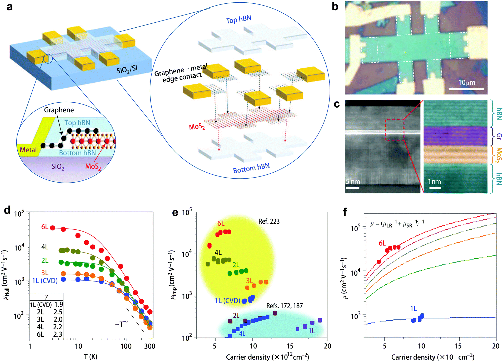 | ||
| Fig. 18 A typical case with combined schemes of mobility engineering. (a) Schematic of the hBN-encapsulated MoS2 multi-terminal device. The exploded view shows the individual components that constitute the heterostructure stack. Bottom: Zoom-in cross-sectional schematic of the metal–graphene–MoS2 contact region. (b) Optical microscope image of a fabricated device. Graphene contact regions are outlined by dashed lines. (c) Cross-sectional TEM image of the fabricated device. The zoom-in false-colour image clearly shows the ultra-sharp interfaces between different layers (graphene, 5L; MoS2, 3L; top hBN, 8 nm; bottom hBN, 19 nm). (d) Hall mobility of hBN-encapsulated MoS2 devices (with different numbers of layers of MoS2) as a function of temperature. The solid fitting lines are drawn by a combined phonon and impurity scattering model. As a visual guide, the dashed line shows the power law μ ∼ T−γ, and fitted values of γ for each device are listed in the inset table. (e) Impurity-limited mobility (μimp) as a function of the MoS2 carrier density. For comparison, previously reported values from MoS2 on SiO2 substrates (ref. 172 and 187) are plotted. (f) The solid lines show the theoretically calculated mobility including both long-range (LR) impurity scattering and short-range (SR) defect scattering based on Matthiessen's rule, μ−1 = μLR−1 + μSR−1, as a function of carrier density for 1L to 6L MoS2. Experimental data are shown as solid circles. Reproduced with permission from ref. 223, copyright 2015, Nature Publishing Group. | ||
While the above results are extracted from the four-terminal measurement, Duan et al. recently confirmed the presence of high performance in the two-terminal measurement, i.e. in the practical FET device configuration, with the similar ‘hBN encapsulation + graphene contact’ scheme. They reported a record high RT mobility of ∼100 cm2 V−1 s−1 and low-T mobility of >300 cm2 V−1 s−1 in hBN sandwiched monolayer MoS2.282 Impressively, extremely high low-temperature two-terminal field-effect mobility of 1300 cm2 V−1 s−1 was observed in multilayer samples.
So far, the highest room temperature mobility that has been achieved in 1L MX2 chalcogenides is in WSe2 with a value of 250 cm2 V−1 s−1. In this case, synergetic engineering on contact optimization by NO2 doping and channel encapsulation by ZrO2 top dielectric was employed. To gain a quick update on the state-of-the-art carrier mobility results achieved to date, Table 6 summarizes the studies with notably high mobility. Apparently, multiple schemes of mobility engineering are used for most of them, pointing out a clear direction for performance optimization and device design.
| Channel material | Channel thickness | Contact and doping | Thermal annealing | Dielectric and encapsulation | Measurement pressure | μ near RT cm2 V−1 s−1 | μ at LT cm2 V−1 s−1 | γ value near RT | Ref. |
|---|---|---|---|---|---|---|---|---|---|
| Abbreviations and notes are the same as Table 3 | |||||||||
| MoS2 | 1L | Gr. | No | DE:BN | vac. | ∼100 | 328 (1.9 K) | 1.2 | 282 |
| MoS2 | 1L | Ti/Pd | ex. 350 °C | DE:SAM | ∼1.3 mPa | 81 | >300 (10 K) | 0.72 | 222 |
| MoS2 | 1L | Ti/Pd | in. 77 °C | DE:SAM | ∼1.3 mPa | 81 | >300 (10 K) | 0.72 | 222 |
| MoS2 | 1L | Au | No | BG:SiO2 | <0.3 mPa | 60–70 | ∼110 (∼5 K) | 0.62 | 221 |
| MoS2-C | 1L | Gr. | DE:BN | vac. | ∼50 | 1020 (∼4 K) | 1.9 | 223 | |
| MoS2-C | 1L | Au | in. 120 °C | BG:SiO2 | vac. (PPMS) | 45 | ∼500 (10 K) | 0.62 | 225 |
| MoS2 | 2L | Gr. | DE:BN | vac. | ∼40 | ∼4000 (∼4 K) | 2.5 | 223 | |
| MoS2 | 3L | Gr. | DE:BN | vac. | ∼40 | ∼2000 (∼4 K) | 2 | 223 | |
| MoS2 | 4L | Gr. | DE:BN | vac. | ∼55 | ∼7000 (∼4 K) | 2.2 | 223 | |
| MoS2 | 5L | Gr. | No | DE:BN | vac. | <100 | 1300 (∼10 K) | N.A. | 282 |
| MoS2 | 6L | Gr. | DE:BN | vac. | ∼120 | 34000 (∼4 K) |
2.3 | 223 | |
| WSe2 | 1L | Ag | in. 170 °C | BG:SiO2 | <0.1 mPa | 140 | N.A. | N.A. | 279 |
| WSe2:p | 1L | Pd + NO2 | N.A. | TG:ZrO2 | <0.1 mPa | 250 | N.A. | N.A. | 280 |
6 Experimental traps and standards
Modern sciences are highly developed and involve interdisciplinary research activities. As for the research field of 2D vdW crystals, numerous chemists, physicists and materials scientists participated into this extremely active subject and stimulated inspirations. However, the lack of solid training on a specific field tends to cause low-level mistakes. Here we would like to point out some apparent ‘traps’ and emphasize some basic experimental standards one should follow.6.1 Mobility overestimation in a dual-gated structure
A common trap in early times is the mobility overestimation in a dual-gated FET structure, pointed out by Fuhrer and Hone.126Fig. 19a illustrates the layout of capacitance for a dual-gated FET geometry. The capacitive coupling between the back and top gates through the large measurement pads of the top gate can lead to a significant deviation of the back-gate capacitance from its nominal parallel-plate value. In a typical device with a thin (few tens nm) high-κ top-gate dielectric, 300 nm bottom gate dielectric, and ∼(100 μm)2 measurement pads, Cpad ≫ CTG ≫ CBG. If the device is characterized by sweeping the back gate with floating the top-gate electrode, then the effective back-gate capacitance C = CBG + (CTG−1 + Cpad−1)−1 ≈ CTG. Neglecting this coupling would lead to a mobility overestimation by a factor of around CTG/CBG. This hidden trap has led to mobility overestimation in several early reports.81,106,181,293 As suggested by Fuhrer and Hone,126 the correct measurement method for the dual-gated FET structure is to sweep one gate while grounding the other one such that removing the capacitive coupling effect. | ||
| Fig. 19 (a) Layout of capacitance distribution in a dual-gate FET. Reproduced with permission from ref. 126, copyright 2013, Nature Publishing Group. (b) A typical four-terminal geometry with a comparable edge distance (Ledge) to the width of voltage probe (Wp), which may cause large overestimation in mobility due to the current crowding effect in the inner voltage probes. (c) A standard four-wire geometry in which Ledge > 10 Wp such that the measurement error can be controlled less than 10%. (d) Extraction barrier height ϕSB under the flat band condition. Reproduced with permission from ref. 181, copyright 2013, American Chemical Society. | ||
6.2 Four-terminal measurement
It is often to adopt the four-terminal geometry in electronic characterization to rule out the contact issue, which may also produce experimental artifacts in some cases. The size of the exfoliated 2D vdW flakes is typically small, which often restricts one to define a long enough distance between the inner voltage collection probes. Fig. 19b shows a typical four-terminal layout used in experiment with comparable probe width and probe distance, which would cause a large experimental error. Normally one defines the channel length by calculating the distance between the midpoints (Lmid) rather than between the near edges (Ledge) of the voltage probes. As will be seen, (Ledge) is slightly shorter but more close to the realistic channel length in most cases. Large mobility overestimation (∼2 folds) would arise if the probe width (Wp) is comparable to Ledge, as shown in Fig. 18b.193,223Taking into account the current crowding effect discussed in Section 4.1.2, the real channel length should be Ledge + 2LT, where LT is the transfer length. LT is typically in the range of about 20–600 nm (dependent on channel thickness and gate bias) for the Au or Ti contacted MoS2179,232 and it is expected to be much smaller if considering the smaller ρc for the graphene/MoS2 contacts.223 Since LT < Ledge, a more accurate channel length should be Ledge rather than the normally used Lmid (∼2Ledge if Wp ∼ Ledge). In a standard four-terminal measurement, the ratio of Ledge to Wp should be greater than 10 to guarantee an experimental error within 10%, as shown in Fig. 6a and 19c.
6.3 Barrier height extraction by thermionic emission
It is frequent to estimate the contact barrier height by using the thermionic emission theory | (16) |
IDS = ln(AT2) + q(ϕSB − VDS)/(kBT) to extract the barrier height at large VDS. For the two-terminal FETs, the basic assumptions which validate the use of the Arrhenius plot to extract barrier height are: (1) contact dominates the overall device current; and (2) thermally assisted tunneling current is negligible. The verification of the two assumptions has been neglected in a large number of reports. For instance, the derivation of a negative barrier height of −5.7 meV at the permalloy/MoS2 contacts contradicts the first assumption and thus is unreliable.184 It is well known that the barrier is effective for carrier blocking only when it is higher than 3kBT. If the extracted barrier height is smaller than 3kBT, ∼80 meV at RT, one has to consider the validity of the original assumptions.
It has been shown that for general long-channel MX2 devices the contact resistance comprises 10–20% of the total resistance,179 indicating the inapplicability to apply this method in most devices. To make the first assumption valid, one has to use an ultrashort channel (e.g. 50 nm long) such that the contact resistance exceeds the channel resistance. Another way to avoid the first assumption is to directly use the net contact results extracted from the four-terminal223,294 or transfer-line measurement (Fig. 8a).229
In addition, the current injection is controlled by two components: thermionic and tunneling. The ratio between them varies with the carrier density (i.e. gate bias). At high carrier density, the channel current actually comprises a high ratio of the tunneling current, which would lead to underestimation of the barrier height by using the Arrhenius plot. One may also notice that the extracted barrier value highly depends on gate bias, a signature of the involvement of tunneling current (since it is gate-bias dependent). In this sense, the extracted barrier value at the high current regime can at most be viewed as an effective parameter.
In order to suppress the tunneling component, one has to tune the device to the flat band condition. Fig. 19d shows the extracted barrier height versus gate bias. Apparently, the presence of tunneling current results in underestimation of the barrier height. As suggested by Appenzeller et al.,181 a more accurate way is to plot the effective barrier height versus gate voltage and extract the turning point between the sublinear and linear regime. The value at the turning point can be more reliably adopted as the barrier height than those extracted in the conventional way.
7 Summary and outlook
The last few years have witnessed the significant progress on the electronic performance of 2D vdW semiconductors. With fundamental understanding in the transport physics and developing delicate mobility engineering strategies, their room temperature mobility increases rapidly from few to few 100 cm2 V−1 s−1. While most mobility engineering efforts are devoted to device fabrication that rely on physical methods (i.e., thermal annealing, energy level matching, hBN encapsulation, and graphene contact), the chemical strategies concerning interfacial and molecular engineering remains highly unexplored.Interface modification by growing self-assembled monolayers (SAMs) on dielectric supports196,222 is a very promising method to create structurally well-defined surfaces with controlled chemical and physical properties like composition, surface energy, hydrophobicity, etc. The use of silane chemistry allows to chemisorb alkyl substituted molecules on SiO2 or other oxide dielectrics and to have an atomically smooth SAM surfaces as ad hoc support for the 2D channels in the interelectrodic channel, which is expected to minimize the density of interfacial impurities and thus the extrinsic impurity scattering. Besides, by virtue of the molecular design and engineering, more advanced functional molecules and convenient defect healing techniques are to be exploited, in order to repair the high-density chalcogen vacancies in the channels. The importance of molecular engineering is also reflected by the requirement for degenerate doping at the contact area. A long-term stable doping onto the ultrathin channels is the key for realizing practical high-performance devices. In the framework of holistic mobility engineering strategies, we expect that the electronic performance of 2D vdW semiconductors will be further propelled to the level of their intrinsic behavior. In this regard, the molecular and interfacial chemistry is a key direction to be exploited for realizing the atomic electronics.
We then remark on the potential of 2D chalcogenides in the atomic electronics in terms of the electronic performance. In deeply downscaled bulk silicon FETs, the channels are heavily doped to reduce the depletion length and thus the channel mobility degrades accordingly due to the scattering from high-density dopants inside. The hole and electron mobility is only about 200–300 cm2 V−1 s−1.295 In FETs made of ultrathin 2D channels, they operate in a fully depleted mode and only light doping is required. No considerable mobility degradation is expected to occur. From the engineering point of view, any 2D semiconductor could be electronically favorable in constructing FETs if the mobility is higher than or approaches the value of heavily doped silicon FETs. Recently a high hole mobility of 250 cm2 V−1 s−1 has been reached in monolayer WSe2 at room temperature,280 indicating that 2D semiconductors are electronically promising for next-generation microelectronics.
Apart from the applications in integrated circuits, the constant improvement on mobility would also benefit the 2D vdW semiconductors for other applications where the thickness of the monolayer is not necessarily required, such as for the radio frequency circuits and the driving FET arrays in flat-panel displays.130 For instance, from multilayer MoS2 flakes it is easy to achieve a high mobility of 100 cm2 V−1 s−1 that is generally higher than the prevailing amorphous silicon, InGaZnO,296–299 and actively developed organic materials.
Furthermore, the elevated electronic performance would be favorable for broad potential applications in optoelectronics such as monolayer light emitting diodes, photodetectors and gas sensors. In general, higher mobility would allow for higher operating current and device performance. In particular if molecules with self-assembly ability on the vdW semiconductors can be developed, novel superlattices with periodic molecule/vdW material structure and designed functions would be possible. In this sense, the mobility engineering can extend the application fields of 2D vdW semiconductors. With constant mobility and molecular engineering, we believe that 2D vdW semiconductors would generate numerous novel applications in near future.
In conclusion, we reviewed recent progress on the charge transport properties of FETs based on 2D chalcogenide semiconductors, in particular by unraveling the role of thickness on their carrier mobility. We discussed the physical origins and strategies devised for mobility engineering, with the ultimate goal of developing device with performance beyond the state-of-the-art. Specifically, various Coulomb impurities including gaseous adsorbates, dangling bonds/chemical groups of dielectric and other surficial residues are the main scattering centers. Contact quality also plays a role as crucial as Coulomb impurities that affects mobility. Besides, vacancy healing could be used as an additional strategy to further improve device performance when both the contact and interface surroundings are optimized. The synergistic improvement of fundamental physico-chemical properties of 2D chalcogenides (chemical composition, spatial distribution and nature of structural and electronic defects) and their interfacing with chemically optimized dielectric supports and functionalized electrodes (to suppress scattering centers, to tailor their environment, and to optimize contact resistance via lowering injection barrier), is the best solution to improve carrier mobility. We conclude that all the above adverse transport factors have to be optimized or suppressed in order to achieve technologically viable atomically thin body FETs and other novel (opto)electronic devices. The review sheds an in-depth light on the charge transport behavior of the 2D semiconductors and would guide future performance optimization and device design.
Acknowledgements
We acknowledge financial support from the European Commission through the Graphene Flagship (GA-604391), the FET project UPGRADE (No. 309056), the Agence Nationale de la Recherche through the LabEx project Nanostructures in Interaction with their Environment (ANR-11-LABX-0058_NIE), the Japan Society for the Promotion of Science (JSPS) through the Grant-in-Aid for Scientific Research (Kakenhi No. 25107004), and the International Center for Frontier Research in Chemistry (icFRC).References
- M. Whittingham, Prog. Solid State Chem., 1978, 12, 41–99 CrossRef CAS.
- M. Whittingham, Chem. Rev., 2004, 104, 4271–4301 CrossRef CAS PubMed.
- K. Novoselov, A. Geim, S. Morozov, D. Jiang, Y. Zhang, S. Dubonos, I. Grigorieva and A. Firsov, Science, 2004, 306, 666–669 CrossRef CAS PubMed.
- K. Novoselov, A. Geim, S. Morozov, D. Jiang, M. Katsnelson, I. Grigorieva, S. Dubonos and A. Firsov, Nature, 2005, 438, 197–200 CrossRef CAS PubMed.
- Y. Zhang, Y. Tan, H. Stormer and P. Kim, Nature, 2005, 438, 201–204 CrossRef CAS PubMed.
- A. K. Geim and K. S. Novoselov, Nat. Mater., 2007, 6, 183–191 CrossRef CAS PubMed.
- A. K. Geim, Science, 2009, 324, 1530–1534 CrossRef CAS PubMed.
- J. A. Wilson and A. D. Yoffe, Adv. Phys., 1969, 18, 193–335 CrossRef CAS.
- A. Yoffe, Adv. Phys., 2002, 51, 799–890 CrossRef.
- R. Mas-Balleste, C. Gomez-Navarro, J. Gomez-Herrero and F. Zamora, Nanoscale, 2011, 3, 20–30 RSC.
- A. H. C. Neto and K. Novoselov, Rep. Prog. Phys., 2011, 74, 082501 CrossRef.
- D. Hewak, Nat. Photonics, 2011, 5, 474 CrossRef.
- Q. H. Wang, K. Kalantar-Zadeh, A. Kis, J. N. Coleman and M. S. Strano, Nat. Nanotechnol., 2012, 7, 699–712 CrossRef CAS PubMed.
- S. Z. Butler, S. M. Hollen, L. Cao, Y. Cui, J. A. Gupta, H. R. Gutiérrez, T. F. Heinz, S. S. Hong, J. Huang, A. F. Ismach, E. Johnston-Halperin, M. Kuno, V. V. Plashnitsa, R. D. Robinson, R. S. Ruoff, S. Salahuddin, J. Shan, L. Shi, M. G. Spencer, M. Terrones, W. Windl and J. E. Goldberger, ACS Nano, 2013, 7, 2898–2926 CrossRef CAS PubMed.
- M. Xu, T. Liang, M. Shi and H. Chen, Chem. Rev., 2013, 113, 3766–3798 CrossRef CAS PubMed.
- M. Chhowalla, H. S. Shin, G. Eda, L.-J. Li, K. P. Loh and H. Zhang, Nat. Chem., 2013, 5, 263–275 CrossRef PubMed.
- J. Pu, L.-J. Li and T. Takenobu, Phys. Chem. Chem. Phys., 2014, 16, 14996–15006 RSC.
- A. B. Kaul, J. Mater. Res., 2014, 29, 348–361 CrossRef CAS.
- G. Fiori, F. Bonaccorso, G. Iannaccone, T. Palacios, D. Neumaier, A. Seabaugh, S. K. Banerjee and L. Colombo, Nat. Nanotechnol., 2014, 9, 768–779 CrossRef CAS PubMed.
- M. Pumera, Z. Sofer and A. Ambrosi, J. Mater. Chem. A, 2014, 2, 8981–8987 CAS.
- D. Jariwala, V. K. Sangwan, L. J. Lauhon, T. J. Marks and M. C. Hersam, ACS Nano, 2014, 8, 1102–1120 CrossRef CAS PubMed.
- R. Ganatra and Q. Zhang, ACS Nano, 2014, 8, 4074–4099 CrossRef CAS PubMed.
- F. Schwierz, J. Pezoldt and R. Granzner, Nanoscale, 2015, 7, 8261–8283 RSC.
- X. Duan, C. Wang, A. Pan, R. Yu and X. Duan, Chem. Soc. Rev., 2015 10.1039/C5CS00507H.
- S. Najmaei, J. Yuan, J. Zhang, P. Ajayan and J. Lou, Acc. Chem. Res., 2015, 48, 31–40 CrossRef CAS PubMed.
- D. Lembke, S. Bertolazzi and A. Kis, Acc. Chem. Res., 2015, 48, 100–110 CrossRef CAS PubMed.
- Y. Shi, H. Li and L.-J. Li, Chem. Soc. Rev., 2015, 44, 2744–2756 RSC.
- Q. Ji, Y. Zhang, Y. Zhang and Z. Liu, Chem. Soc. Rev., 2015, 44, 2587–2602 RSC.
- H. Wang, H. Yuan, S. Sae Hong, Y. Li and Y. Cui, Chem. Soc. Rev., 2015, 44, 2664–2680 RSC.
- F. Wang, Z. X. Wang, Q. S. Wang, F. M. Wang, L. Yin, K. Xu, Y. Huang and J. He, Nanotechnology, 2015, 26, 292001 CrossRef PubMed.
- A. C. Ferrari, F. Bonaccorso, V. Fal'ko, K. S. Novoselov, S. Roche, P. Boggild, S. Borini, F. H. L. Koppens, V. Palermo, N. Pugno, J. A. Garrido, R. Sordan, A. Bianco, L. Ballerini, M. Prato, E. Lidorikis, J. Kivioja, C. Marinelli, T. Ryhanen, A. Morpurgo, J. N. Coleman, V. Nicolosi, L. Colombo, A. Fert, M. Garcia-Hernandez, A. Bachtold, G. F. Schneider, F. Guinea, C. Dekker, M. Barbone, Z. Sun, C. Galiotis, A. N. Grigorenko, G. Konstantatos, A. Kis, M. Katsnelson, L. Vandersypen, A. Loiseau, V. Morandi, D. Neumaier, E. Treossi, V. Pellegrini, M. Polini, A. Tredicucci, G. M. Williams, B. Hee Hong, J.-H. Ahn, J. Min Kim, H. Zirath, B. J. van Wees, H. van der Zant, L. Occhipinti, A. Di Matteo, I. A. Kinloch, T. Seyller, E. Quesnel, X. Feng, K. Teo, N. Rupesinghe, P. Hakonen, S. R. T. Neil, Q. Tannock, T. Lofwander and J. Kinaret, Nanoscale, 2015, 7, 4598–4810 RSC.
- H. Schmidt, F. Giustiniano and G. Eda, Chem. Soc. Rev., 2015, 44, 7715–7736 RSC.
- B. Peng, P. K. Ang and K. P. Loh, Nano Today, 2015, 10, 128–137 CrossRef CAS.
- H. Zeng and X. Cui, Chem. Soc. Rev., 2015, 44, 2629–2642 RSC.
- X. Zhang, X.-F. Qiao, W. Shi, J.-B. Wu, D.-S. Jiang and P.-H. Tan, Chem. Soc. Rev., 2015, 44, 2757–2785 RSC.
- M. Buscema, J. O. Island, D. J. Groenendijk, S. I. Blanter, G. A. Steele, H. S. J. van der Zant and A. Castellanos-Gomez, Chem. Soc. Rev., 2015, 44, 3691–3718 RSC.
- F. Al-Alamy and A. Balchin, J. Cryst. Growth, 1977, 38, 221–232 CrossRef CAS.
- Y. Feldman, E. Wasserman, D. J. Srolovitz and R. Tenne, Science, 1995, 267, 222–225 CrossRef CAS PubMed.
- I. Jen-La Plante, T. W. Zeid, P. Yang and T. Mokari, J. Mater. Chem., 2010, 20, 6612–6617 RSC.
- D. Kim, D. Sun, W. Lu, Z. Cheng, Y. Zhu, D. Le, T. S. Rahman and L. Bartels, Langmuir, 2011, 27, 11650–11653 CrossRef CAS PubMed.
- H. Jin, D. Cheng, J. Li, X. Cao, B. Li, X. Wang, X. Liu and X. Zhao, Solid State Sci., 2011, 13, 1166–1171 CrossRef CAS.
- K.-K. Liu, W. Zhang, Y.-H. Lee, Y.-C. Lin, M.-T. Chang, C. Su, C.-S. Chang, H. Li, Y. Shi, H. Zhang, C.-S. Lai and L.-J. Li, Nano Lett., 2012, 12, 1538–1544 CrossRef CAS PubMed.
- Y. Shi, W. Zhou, A.-Y. Lu, W. Fang, Y.-H. Lee, A. L. Hsu, S. M. Kim, K. K. Kim, H. Y. Yang, L.-J. Li, J.-C. Idrobo and J. Kong, Nano Lett., 2012, 12, 2784–2791 CrossRef CAS PubMed.
- S. Balendhran, J. Z. Ou, M. Bhaskaran, S. Sriram, S. Ippolito, Z. Vasic, E. Kats, S. Bhargava, S. Zhuiykov and K. Kalantar-zadeh, Nanoscale, 2012, 4, 461–466 RSC.
- S. Ding, D. Zhang, J. S. Chen and X. W. D. Lou, Nanoscale, 2012, 4, 95–98 RSC.
- Y. Zhan, Z. Liu, S. Najmaei, P. M. Ajayan and J. Lou, Small, 2012, 8, 966–971 CrossRef CAS PubMed.
- Y.-H. Lee, X.-Q. Zhang, W. Zhang, M.-T. Chang, C.-T. Lin, K.-D. Chang, Y.-C. Yu, J. T.-W. Wang, C.-S. Chang, L.-J. Li and T.-W. Lin, Adv. Mater., 2012, 24, 2320–2325 CrossRef CAS PubMed.
- X. Wang, H. Feng, Y. Wu and L. Jiao, J. Am. Chem. Soc., 2013, 135, 5304–5307 CrossRef CAS PubMed.
- W. Wu, D. De, S.-C. Chang, Y. Wang, H. Peng, J. Bao and S.-S. Pei, Appl. Phys. Lett., 2013, 102, 142106 CrossRef.
- S. Lei, L. Ge, Z. Liu, S. Najmaei, G. Shi, G. You, J. Lou, R. Vajtai and P. M. Ajayan, Nano Lett., 2013, 13, 2777–2781 CrossRef CAS PubMed.
- S. Wu, C. Huang, G. Aivazian, J. S. Ross, D. H. Cobden and X. Xu, ACS Nano, 2013, 7, 2768–2772 CrossRef CAS PubMed.
- Y.-H. Lee, L. Yu, H. Wang, W. Fang, X. Ling, Y. Shi, C.-T. Lin, J.-K. Huang, M.-T. Chang, C.-S. Chang, M. Dresselhaus, T. Palacios, L.-J. Li and J. Kong, Nano Lett., 2013, 13, 1852–1857 CAS.
- L. Huang, Y. Yu, C. Li and L. Cao, J. Phys. Chem. C, 2013, 117, 6469–6475 CAS.
- Y. Yu, C. Li, Y. Liu, L. Su, Y. Zhang and L. Cao, Sci. Rep., 2013, 3, 1866 Search PubMed.
- X. Lu, M. I. B. Utama, J. Lin, X. Gong, J. Zhang, Y. Zhao, S. T. Pantelides, J. Wang, Z. Dong, Z. Liu, W. Zhou and Q. Xiong, Nano Lett., 2014, 14, 2419–2425 CrossRef CAS PubMed.
- Q. Ma, M. Isarraraz, C. S. Wang, E. Preciado, V. Klee, S. Bobek, K. Yamaguchi, E. Li, P. M. Odenthal, A. Nguyen, D. Barroso, D. Sun, G. von Son Palacio, M. Gomez, A. Nguyen, D. Le, G. Pawin, J. Mann, T. F. Heinz, T. S. Rahman and L. Bartels, ACS Nano, 2014, 8, 4672–4677 CrossRef CAS PubMed.
- J. Mann, Q. Ma, P. M. Odenthal, M. Isarraraz, D. Le, E. Preciado, D. Barroso, K. Yamaguchi, G. von Son Palacio, A. Nguyen, T. Tran, M. Wurch, A. Nguyen, V. Klee, S. Bobek, D. Sun, T. F. Heinz, T. S. Rahman, R. Kawakami and L. Bartels, Adv. Mater., 2014, 26, 1399–1404 CrossRef CAS PubMed.
- H. Li, X. Duan, X. Wu, X. Zhuang, H. Zhou, Q. Zhang, X. Zhu, W. Hu, P. Ren, P. Guo, L. Ma, X. Fan, X. Wang, J. Xu, A. Pan and X. Duan, J. Am. Chem. Soc., 2014, 136, 3756–3759 CrossRef CAS PubMed.
- J.-K. Huang, J. Pu, C.-L. Hsu, M.-H. Chiu, Z.-Y. Juang, Y.-H. Chang, W.-H. Chang, Y. Iwasa, T. Takenobu and L.-J. Li, ACS Nano, 2014, 8, 923–930 CrossRef CAS PubMed.
- A. S. George, Z. Mutlu, R. Ionescu, R. J. Wu, J. S. Jeong, H. H. Bay, Y. Chai, K. A. Mkhoyan, M. Ozkan and C. S. Ozkan, Adv. Funct. Mater., 2014, 24, 7461–7466 CrossRef CAS.
- X. Wang, Y. Gong, G. Shi, W. L. Chow, K. Keyshar, G. Ye, R. Vajtai, J. Lou, Z. Liu, E. Ringe, B. K. Tay and P. M. Ajayan, ACS Nano, 2014, 8, 5125–5131 CrossRef CAS PubMed.
- Y.-C. Lin, N. Lu, N. Perea-Lopez, J. Li, Z. Lin, X. Peng, C. H. Lee, C. Sun, L. Calderin, P. N. Browning, M. S. Bresnehan, M. J. Kim, T. S. Mayer, M. Terrones and J. A. Robinson, ACS Nano, 2014, 8, 3715–3723 CrossRef CAS PubMed.
- C. M. Orofeo, S. Suzuki, Y. Sekine and H. Hibino, Appl. Phys. Lett., 2014, 105, 083112 CrossRef.
- Y. Gong, Z. Liu, A. R. Lupini, G. Shi, J. Lin, S. Najmaei, Z. Lin, A. L. Elias, A. Berkdemir, G. You, H. Terrones, M. Terrones, R. Vajtai, S. T. Pantelides, S. J. Pennycook, J. Lou, W. Zhou and P. M. Ajayan, Nano Lett., 2014, 14, 442–449 CrossRef CAS PubMed.
- C.-C. Huang, F. Al-Saab, Y. Wang, J.-Y. Ou, J. C. Walker, S. Wang, B. Gholipour, R. E. Simpson and D. W. Hewak, Nanoscale, 2014, 6, 12792–12797 RSC.
- J. Zhang, H. Yu, W. Chen, X. Tian, D. Liu, M. Cheng, G. Xie, W. Yang, R. Yang, X. Bai, D. Shi and G. Zhang, ACS Nano, 2014, 8, 6024–6030 CrossRef CAS PubMed.
- X. Ling, Y.-H. Lee, Y. Lin, W. Fang, L. Yu, M. S. Dresselhaus and J. Kong, Nano Lett., 2014, 14, 464–472 CrossRef CAS PubMed.
- Y. Lee, J. Lee, H. Bark, I.-K. Oh, G. H. Ryu, Z. Lee, H. Kim, J. H. Cho, J.-H. Ahn and C. Lee, Nanoscale, 2014, 6, 2821–2826 RSC.
- A. Tarasov, P. M. Campbell, M.-Y. Tsai, Z. R. Hesabi, J. Feirer, S. Graham, W. J. Ready and E. M. Vogel, Adv. Funct. Mater., 2014, 24, 6389–6400 CrossRef CAS.
- M. Zhang, J. Wu, Y. Zhu, D. O. Dumcenco, J. Hong, N. Mao, S. Deng, Y. Chen, Y. Yang, C. Jin, S. H. Chaki, Y.-S. Huang, J. Zhang and L. Xie, ACS Nano, 2014, 8, 7130–7137 CrossRef CAS PubMed.
- G. H. Han, N. J. Kybert, C. H. Naylor, B. S. Lee, J. Ping, J. H. Park, J. Kang, S. Y. Lee, Y. H. Lee, R. Agarwal and A. T. C. Johnson, Nat. Commun., 2015, 6, 6128 CrossRef CAS PubMed.
- S. J. Yun, S. H. Chae, H. Kim, J. C. Park, J.-H. Park, G. H. Han, J. S. Lee, S. M. Kim, H. M. Oh, J. Seok, M. S. Jeong, K. K. Kim and Y. H. Lee, ACS Nano, 2015, 9, 5510–5519 CrossRef CAS PubMed.
- A. Pisoni, J. Jacimovic, O. S. Barisic, A. Walter, B. Nafradi, P. Bugnon, A. Magrez, H. Berger, Z. Revay and L. Forro, J. Phys. Chem. C, 2015, 119, 3918–3922 CAS.
- J. Jeon, S. K. Jang, S. M. Jeon, G. Yoo, Y. H. Jang, J.-H. Park and S. Lee, Nanoscale, 2015, 7, 1688–1695 RSC.
- J. Tao, J. Chai, X. Lu, L. M. Wong, T. I. Wong, J. Pan, Q. Xiong, D. Chi and S. Wang, Nanoscale, 2015, 7, 2497–2503 RSC.
- J. Park, N. Choudhary, J. Smith, G. Lee, M. Kim and W. Choi, Appl. Phys. Lett., 2015, 106, 012104 CrossRef.
- V. K. Kumar, S. Dhar, T. H. Choudhury, S. A. Shivashankar and S. Raghavan, Nanoscale, 2015, 7, 7802–7810 RSC.
- K. Kang, S. Xie, L. Huang, Y. Han, P. Y. Huang, K. F. Mak, C.-J. Kim, D. Muller and J. Park, Nature, 2015, 520, 656–660 CrossRef CAS PubMed.
- L. Britnell, R. V. Gorbachev, R. Jalil, B. D. Belle, F. Schedin, A. Mishchenko, T. Georgiou, M. I. Katsnelson, L. Eaves, S. V. Morozov, N. M. R. Peres, J. Leist, A. K. Geim, K. S. Novoselov and L. A. Ponomarenko, Science, 2012, 335, 947–950 CrossRef CAS PubMed.
- T. Georgiou, R. Jalil, B. D. Belle, L. Britnell, R. V. Gorbachev, S. V. Morozov, Y.-J. Kim, A. Gholinia, S. J. Haigh, O. Makarovsky, L. Eaves, L. A. Ponomarenko, A. K. Geim, K. S. Novoselov and A. Mishchenko, Nat. Nanotechnol., 2013, 8, 100–103 CrossRef CAS PubMed.
- B. Radisavljevic, A. Radenovic, J. Brivio, V. Giacometti and A. Kis, Nat. Nanotechnol., 2011, 6, 147–150 CrossRef CAS PubMed.
- B. Radisavljevic and A. Kis, Nat. Mater., 2013, 12, 815–820 CrossRef CAS PubMed.
- A. K. Geim and I. V. Grigorieva, Nature, 2013, 499, 419–425 CrossRef CAS PubMed.
- T. Cao, G. Wang, W. Han, H. Ye, C. Zhu, J. Shi, Q. Niu, P. Tan, E. Wang, B. Liu and J. Feng, Nat. Commun., 2012, 3, 887 CrossRef PubMed.
- Z. Gong, G.-B. Liu, H. Yu, D. Xiao, X. Cui, X. Xu and W. Yao, Nat. Commun., 2013, 4, 2053 Search PubMed.
- A. M. Jones, H. Yu, N. J. Ghimire, S. Wu, G. Aivazian, J. S. Ross, B. Zhao, J. Yan, D. G. Mandrus, D. Xiao, W. Yao and X. Xu, Nat. Nanotechnol., 2013, 8, 634–638 CrossRef CAS PubMed.
- K. F. Mak, K. He, J. Shan and T. F. Heinz, Nat. Nanotechnol., 2012, 7, 494–498 CrossRef CAS PubMed.
- R. Suzuki, M. Sakano, Y. J. Zhang, R. Akashi, D. Morikawa, A. Harasawa, K. Yaji, K. Kuroda, K. Miyamoto, T. Okuda, K. Ishizaka, R. Arita and Y. Iwasa, Nat. Nanotechnol., 2014, 9, 611–617 CrossRef CAS PubMed.
- H. Zeng, J. Dai, W. Yao, D. Xiao and X. Cui, Nat. Nanotechnol., 2012, 7, 490–493 CrossRef CAS PubMed.
- D. Akinwande, N. Petrone and J. Hone, Nat. Commun., 2014, 5, 5678 CrossRef CAS PubMed.
- W. J. Yu, Y. Liu, H. Zhou, A. Yin, Z. Li, Y. Huang and X. Duan, Nat. Nanotechnol., 2013, 8, 952–958 CrossRef CAS PubMed.
- X. Duan, C. Wang, J. C. Shaw, R. Cheng, Y. Chen, H. Li, X. Wu, Y. Tang, Q. Zhang, A. Pan, J. Jiang, R. Yu, Y. Huang and X. Duan, Nat. Nanotechnol., 2014, 9, 1024–1030 CrossRef CAS PubMed.
- H. S. Lee, S.-W. Min, Y.-G. Chang, M. K. Park, T. Nam, H. Kim, J. H. Kim, S. Ryu and S. Im, Nano Lett., 2012, 12, 3695–3700 CrossRef CAS PubMed.
- O. Lopez-Sanchez, D. Lembke, M. Kayci, A. Radenovic and A. Kis, Nat. Nanotechnol., 2013, 8, 497–501 CrossRef CAS PubMed.
- D. Jariwala, V. K. Sangwan, C.-C. Wu, P. L. Prabhumirashi, M. L. Geier, T. J. Marks, L. J. Lauhon and M. C. Hersam, Proc. Natl. Acad. Sci. U. S. A., 2013, 110, 18076–18080 CrossRef CAS PubMed.
- L. Britnell, R. M. Ribeiro, A. Eckmann, R. Jalil, B. D. Belle, A. Mishchenko, Y.-J. Kim, R. V. Gorbachev, T. Georgiou, S. V. Morozov, A. N. Grigorenko, A. K. Geim, C. Casiraghi, A. H. C. Neto and K. S. Novoselov, Science, 2013, 340, 1311–1314 CrossRef CAS PubMed.
- M. Bernardi, M. Palummo and J. C. Grossman, Nano Lett., 2013, 13, 3664–3670 CrossRef CAS PubMed.
- F. Xia, H. Wang, D. Xiao, M. Dubey and A. Ramasubramaniam, Nat. Photonics, 2014, 8, 899–907 CrossRef CAS.
- F. H. L. Koppens, T. Mueller, P. Avouris, A. C. Ferrari, M. S. Vitiello and M. Polini, Nat. Nanotechnol., 2014, 9, 780–793 CrossRef CAS PubMed.
- R.-H. Yan, A. Ourmazd and K. Lee, IEEE Trans. Electron Devices, 1992, 39, 1704–1710 CrossRef CAS.
- L. L. Chang, Y. K. Choi, D. W. Ha, P. Ranade, S. Y. Xiong, J. Bokor, C. M. Hu and T. J. King, Proc. IEEE, 2003, 91, 1860–1873 CrossRef CAS.
- M. Ieong, B. Doris, J. Kedzierski, K. Rim and M. Yang, Science, 2004, 306, 2057–2060 CrossRef CAS PubMed.
- E. M. Vogel, Nat. Nanotechnol., 2007, 2, 25–32 CrossRef CAS PubMed.
- ITRS2013, The International Technology Roadmap for Semiconductors, Semiconductor industry association technical report, 2013.
- F. Schwierz, Nat. Nanotechnol., 2010, 5, 487–496 CrossRef CAS PubMed.
- H. Wang, L. Yu, Y.-H. Lee, Y. Shi, A. Hsu, M. L. Chin, L.-J. Li, M. Dubey, J. Kong and T. Palacios, Nano Lett., 2012, 12, 4674–4680 CrossRef CAS PubMed.
- L. Gomez, I. Aberg and J. L. Hoyt, IEEE Electron Device Lett., 2007, 28, 285–287 CrossRef CAS.
- H. Sakaki, T. Noda, K. Hirakawa, M. Tanaka and T. Matsusue, Appl. Phys. Lett., 1987, 51, 1934–1936 CrossRef CAS.
- A. Gold, Phys. Rev. B: Condens. Matter Mater. Phys., 1987, 35, 723–733 CrossRef CAS.
- L. Tao, E. Cinquanta, D. Chiappe, C. Grazianetti, M. Fanciulli, M. Dubey, A. Molle and D. Akinwande, Nat. Nanotechnol., 2015, 10, 227–231 CrossRef CAS PubMed.
- A. Ayari, E. Cobas, O. Ogundadegbe and M. S. Fuhrer, J. Appl. Phys., 2007, 101, 014507 CrossRef.
- R. Sordan, F. Traversi and V. Russo, Appl. Phys. Lett., 2009, 94, 073305 CrossRef.
- F. Traversi, V. Russo and R. Sordan, Appl. Phys. Lett., 2009, 94, 223312 CrossRef.
- S.-L. Li, H. Miyazaki, A. Kumatani, A. Kanda and K. Tsukagoshi, Nano Lett., 2010, 10, 2357–2362 CrossRef CAS PubMed.
- N. Harada, K. Yagi, S. Sato and N. Yokoyama, Appl. Phys. Lett., 2010, 96, 012102 CrossRef.
- S.-L. Li, H. Miyazaki, H. Hiura, C. Liu and K. Tsukagoshi, ACS Nano, 2011, 5, 500–506 CrossRef CAS PubMed.
- L. G. Rizzi, M. Bianchi, A. Behnam, E. Carrion, E. Guerriero, L. Polloni, E. Pop and R. Sordan, Nano Lett., 2012, 12, 3948–3953 CrossRef CAS PubMed.
- E. Guerriero, L. Polloni, M. Bianchi, A. Behnam, E. Carrion, L. G. Rizzi, E. Pop and R. Sordan, ACS Nano, 2013, 7, 5588–5594 CrossRef CAS PubMed.
- S.-L. Li, H. Miyazaki, M. V. Lee, C. Liu, A. Kanda and K. Tsukagoshi, Small, 2011, 7, 1552–1556 CrossRef CAS PubMed.
- H. Miyazaki, S. Li, A. Kanda and K. Tsukagoshi, Semicond. Sci. Technol., 2010, 25, 034008 CrossRef.
- S. Nakaharai, T. Iijima, S. Ogawa, S. Suzuki, S.-L. Li, K. Tsukagoshi, S. Sato and N. Yokoyama, ACS Nano, 2013, 7, 5694–5700 CrossRef CAS PubMed.
- A. Aparecido-Ferreira, H. Miyazaki, S.-L. Li, K. Komatsu, S. Nakaharai and K. Tsukagoshi, Nanoscale, 2012, 4, 7842–7846 RSC.
- H. Miyazaki, S.-L. Li, S. Nakaharai and K. Tsukagoshi, Appl. Phys. Lett., 2012, 100, 163115 CrossRef.
- S. Nakaharai, T. Iijima, S. Ogawa, S. L. Li, K. Tsukagoshi, S. Sato and N. Yokoyama, IEEE Trans. Nanotechnol., 2014, 13, 1039–1043 CrossRef.
- S. Nakaharai, T. Iijima, S. Ogawa, H. Miyazaki, S. Li, K. Tsukagoshi, S. Sato and N. Yokoyama, Appl. Phys. Express, 2012, 5, 015101 CrossRef.
- M. S. Fuhrer and J. Hone, Nat. Nanotechnol., 2013, 8, 146–147 CrossRef CAS PubMed.
- R. Fivaz and E. Mooser, Phys. Rev., 1967, 163, 743–755 CrossRef CAS.
- K. Kaasbjerg, K. S. Thygesen and K. W. Jacobsen, Phys. Rev. B: Condens. Matter Mater. Phys., 2012, 85, 115317 CrossRef.
- K. Kaasbjerg, K. S. Thygesen and A. P. Jauho, Phys. Rev. B: Condens. Matter Mater. Phys., 2013, 87, 235312 CrossRef.
- S. Kim, A. Konar, W.-S. Hwang, J. H. Lee, J. Lee, J. Yang, C. Jung, H. Kim, J.-B. Yoo, J.-Y. Choi, Y. W. Jin, S. Y. Lee, D. Jena, W. Choi and K. Kim, Nat. Commun., 2012, 3, 1011 CrossRef PubMed.
- S.-L. Li, K. Wakabayashi, Y. Xu, S. Nakaharai, K. Komatsu, W.-W. Li, Y.-F. Lin, A. Aparecido-Ferreira and K. Tsukagoshi, Nano Lett., 2013, 13, 3546–3552 CrossRef CAS PubMed.
- N. Ma and D. Jena, Phys. Rev. X, 2014, 4, 011043 Search PubMed.
- M. Bouroushian, Electrochemistry of metal chalcogenides, Springer, Berlin, Heidelberg, 2010 Search PubMed.
- S.-L. Li, H. Miyazaki, H. Song, H. Kuramochi, S. Nakaharai and K. Tsukagoshi, ACS Nano, 2012, 6, 7381–7388 CrossRef PubMed.
- Y.-C. Lin, D. O. Dumcenco, Y.-S. Huang and K. Suenaga, Nat. Nanotechnol., 2014, 9, 391–396 CrossRef CAS PubMed.
- S. Cho, S. Kim, J. H. Kim, J. Zhao, J. Seok, D. H. Keum, J. Baik, D.-H. Choe, K. J. Chang, K. Suenaga, S. W. Kim, Y. H. Lee and H. Yang, Science, 2015, 349, 625 CrossRef CAS PubMed.
- R. Kappera, D. Voiry, S. E. Yalcin, B. Branch, G. Gupta, A. D. Mohite and M. Chhowalla, Nat. Mater., 2014, 13, 1128–1134 CrossRef CAS PubMed.
- R. Kappera, D. Voiry, S. E. Yalcin, W. Jen, M. Acerce, S. Torrel, B. Branch, S. Lei, W. Chen, S. Najmaei, J. Lou, P. M. Ajayan, G. Gupta, A. D. Mohite and M. Chhowalla, APL Mater., 2014, 2, 092516 CrossRef.
- D. Voiry, A. Mohite and M. Chhowalla, Chem. Soc. Rev., 2015, 44, 2702–2712 RSC.
- A. Molina-Sanchez and L. Wirtz, Phys. Rev. B: Condens. Matter Mater. Phys., 2011, 84, 155413 CrossRef.
- J. L. Verble and T. J. Wieting, Phys. Rev. Lett., 1970, 25, 362–365 CrossRef CAS.
- T. J. Wieting and J. L. Verble, Phys. Rev. B: Solid State, 1971, 3, 4286–4292 CrossRef.
- O. P. Agnihotr and H. K. Sehgal, Philos. Mag., 1972, 26, 753 CrossRef.
- O. P. Agnihotr, H. K. Sehgal and A. K. Garg, Solid State Commun., 1973, 12, 135–138 CrossRef.
- T. Sekine, M. Izumi, T. Nakashizu, K. Uchinokura and E. Matsuura, J. Phys. Soc. Jpn., 1980, 49, 1069–1077 CrossRef CAS.
- S. Sugai and T. Ueda, Phys. Rev. B: Condens. Matter Mater. Phys., 1982, 26, 6554–6558 CrossRef CAS.
- T. Sekine, K. Uchinokura, T. Nakashizu, E. Matsuura and R. Yoshizaki, J. Phys. Soc. Jpn., 1984, 53, 811–818 CrossRef CAS.
- T. Wieting, A. Grisel and F. Levy, Phys. B, 1980, 99, 337–342 CrossRef CAS.
- T. Sekine, T. Nakashizu, K. Toyoda, K. Uchinokura and E. Matsuura, Solid State Commun., 1980, 35, 371–373 CrossRef CAS.
- C. Sourisseau, F. Cruege, M. Fouassier and M. Alba, Chem. Phys., 1991, 150, 281–293 CrossRef CAS.
- G. Frey, R. Tenne, M. Matthews, M. Dresselhaus and G. Dresselhaus, J. Mater. Res., 1998, 13, 2412–2417 CrossRef CAS.
- C. Lee, H. Yan, L. E. Brus, T. F. Heinz, J. Hone and S. Ryu, ACS Nano, 2010, 4, 2695–2700 CrossRef CAS PubMed.
- H. Terrones, E. D. Corro, S. Feng, J. M. Poumirol, D. Rhodes, D. Smirnov, N. R. Pradhan, Z. Lin, M. A. T. Nguyen, A. L. Elias, T. E. Mallouk, L. Balicas, M. A. Pimenta and M. Terrones, Sci. Rep., 2014, 4, 4215 CAS.
- M. Yamamoto, S. T. Wang, M. Ni, Y.-F. Lin, S.-L. Li, S. Aikawa, W.-B. Jian, K. Ueno, K. Wakabayashi and K. Tsukagoshi, ACS Nano, 2014, 8, 3895–3903 CrossRef CAS PubMed.
- S. Jiménez Sandoval, D. Yang, R. F. Frindt and J. C. Irwin, Phys. Rev. B: Condens. Matter Mater. Phys., 1991, 44, 3955–3962 CrossRef.
- C. Ataca, M. Topsakal, E. Akturk and S. Ciraci, J. Phys. Chem. C, 2011, 115, 16354–16361 CAS.
- J. Ribeiro-Soares, R. M. Almeida, E. B. Barros, P. T. Araujo, M. S. Dresselhaus, L. G. Cançado and A. Jorio, Phys. Rev. B: Condens. Matter Mater. Phys., 2014, 90, 115438 CrossRef.
- Y. Zhao, X. Luo, H. Li, J. Zhang, P. T. Araujo, C. K. Gan, J. Wu, H. Zhang, S. Y. Quek, M. S. Dresselhaus and Q. Xiong, Nano Lett., 2013, 13, 1007–1015 CrossRef CAS PubMed.
- A. Kuc, N. Zibouche and T. Heine, Phys. Rev. B: Condens. Matter Mater. Phys., 2011, 83, 245213 CrossRef.
- W. S. Yun, S. W. Han, S. C. Hong, I. G. Kim and J. D. Lee, Phys. Rev. B: Condens. Matter Mater. Phys., 2012, 85, 033305 CrossRef.
- A. Kumar and P. K. Ahluwalia, Phys. B, 2012, 407, 4627–4634 CrossRef CAS.
- Y. Yoon, K. Ganapathi and S. Salahuddin, Nano Lett., 2011, 11, 3768–3773 CrossRef CAS PubMed.
- A. R. Beal and H. P. Hughes, J. Phys. C: Solid State Phys., 1979, 12, 881 CrossRef CAS.
- C. Yim, M. O'Brien, N. McEvoy, S. Winters, I. Mirza, J. G. Lunney and G. S. Duesberg, Appl. Phys. Lett., 2014, 104, 103114 CrossRef.
- H. Zhang, Y. Ma, Y. Wan, X. Rong, Z. Xie, W. Wang and L. Dai, Sci. Rep., 2015, 5, 8440 CrossRef CAS PubMed.
- B. Mukherjee, F. Tseng, D. Gunlycke, K. K. Amara, G. Eda and E. Simsek, Opt. Mater. Express, 2015, 5, 447–455 CrossRef.
- H.-L. Liu, C.-C. Shen, S.-H. Su, C.-L. Hsu, M.-Y. Li and L.-J. Li, Appl. Phys. Lett., 2014, 105, 201905 CrossRef.
- Y. Li, A. Chernikov, X. Zhang, A. Rigosi, H. M. Hill, A. M. van der Zande, D. A. Chenet, E.-M. Shih, J. Hone and T. F. Heinz, Phys. Rev. B: Condens. Matter Mater. Phys., 2014, 90, 205422 CrossRef.
- D. J. Late, B. Liu, H. S. S. R. Matte, V. P. Dravid and C. N. R. Rao, ACS Nano, 2012, 6, 5635–5641 CrossRef CAS PubMed.
- V. K. Sangwan, H. N. Arnold, D. Jariwala, T. J. Marks, L. J. Lauhon and M. C. Hersam, Nano Lett., 2013, 13, 4351–4355 CrossRef CAS PubMed.
- D. Lembke, A. Allain and A. Kis, Nanoscale, 2015, 7, 6255–6260 RSC.
- B. W. H. Baugher, H. O. H. Churchill, Y. Yang and P. Jarillo-Herrero, Nano Lett., 2013, 13, 4212–4216 CrossRef CAS PubMed.
- L. Chu, H. Schmidt, J. Pu, S. Wang, B. Özyilmaz, T. Takenobu and G. Eda, Sci. Rep., 2014, 4, 7293 CrossRef CAS PubMed.
- J. Kang, W. Liu and K. Banerjee, Appl. Phys. Lett., 2014, 104, 093106 CrossRef.
- G.-H. Lee, Y.-J. Yu, X. Cui, N. Petrone, C.-H. Lee, M. S. Choi, D.-Y. Lee, C. Lee, W. J. Yoo, K. Watanabe, T. Taniguchi, C. Nuckolls, P. Kim and J. Hone, ACS Nano, 2013, 7, 7931–7936 CrossRef CAS PubMed.
- M. Y. Chan, K. Komatsu, S.-L. Li, Y. Xu, P. Darmawan, H. Kuramochi, S. Nakaharai, A. Aparecido-Ferreira, K. Watanabe, T. Taniguchi and K. Tsukagoshi, Nanoscale, 2013, 5, 9572–9576 RSC.
- T. Jin, J. Kang, E. S. Kim, S. Lee and C. Lee, J. Appl. Phys., 2013, 114, 164509 CrossRef.
- A. R. Klots, A. K. M. Newaz, B. Wang, D. Prasai, H. Krzyzanowska, J. Lin, D. Caudel, N. J. Ghimire, J. Yan, B. L. Ivanov, K. A. Velizhanin, A. Burger, D. G. Mandrus, N. H. Tolk, S. T. Pantelides and K. I. Bolotin, Sci. Rep., 2014, 4, 6608 CrossRef CAS PubMed.
- Y. Guo, Y. Han, J. Li, A. Xiang, X. Wei, S. Gao and Q. Chen, ACS Nano, 2014, 8, 7771–7779 CrossRef CAS PubMed.
- H. Qiu, L. Pan, Z. Yao, J. Li, Y. Shi and X. Wang, Appl. Phys. Lett., 2012, 100, 123104 CrossRef.
- S. Das, H.-Y. Chen, A. V. Penumatcha and J. Appenzeller, Nano Lett., 2013, 13, 100–105 CrossRef CAS PubMed.
- M. M. Perera, M.-W. Lin, H.-J. Chuang, B. P. Chamlagain, C. Wang, X. Tan, M. M.-C. Cheng, D. Tománek and Z. Zhou, ACS Nano, 2013, 7, 4449–4458 CrossRef CAS PubMed.
- H. Fang, M. Tosun, G. Seol, T. C. Chang, K. Takei, J. Guo and A. Javey, Nano Lett., 2013, 13, 1991–1995 CrossRef CAS PubMed.
- W. Wang, Y. Liu, L. Tang, Y. Jin, T. Zhao and F. Xiu, Sci. Rep., 2014, 4, 6928 CrossRef CAS PubMed.
- J. Pu, Y. Yomogida, K.-K. Liu, L.-J. Li, Y. Iwasa and T. Takenobu, Nano Lett., 2012, 12, 4013–4017 CrossRef CAS PubMed.
- X. Zou, J. Wang, C.-H. Chiu, Y. Wu, X. Xiao, C. Jiang, W.-W. Wu, L. Mai, T. Chen, J. Li, J. C. Ho and L. Liao, Adv. Mater., 2014, 26, 6255–6261 CrossRef CAS PubMed.
- A. T. Neal, H. Liu, J. Gu and P. D. Ye, ACS Nano, 2013, 7, 7077–7082 CrossRef CAS PubMed.
- H. Liu, A. T. Neal and P. D. Ye, ACS Nano, 2012, 6, 8563–8569 CrossRef CAS PubMed.
- T. Roy, M. Tosun, J. S. Kang, A. B. Sachid, S. B. Desai, M. Hettick, C. C. Hu and A. Javey, ACS Nano, 2014, 8, 6259–6264 CrossRef CAS PubMed.
- Y. Zhang, J. T. Ye, Y. Matsuhashi and Y. Iwasa, Nano Lett., 2012, 12, 1136–1140 CrossRef CAS PubMed.
- J. Na, M.-K. Joo, M. Shin, J. Huh, J.-S. Kim, M. Piao, J.-E. Jin, H.-K. Jang, H. J. Choi, J. H. Shim and G.-T. Kim, Nanoscale, 2014, 6, 433–441 RSC.
- F. Wang, P. Stepanov, M. Gray and C. N. Lau, Nanotechnology, 2015, 26, 105709 CrossRef PubMed.
- N. R. Pradhan, D. Rhodes, Q. Zhang, S. Talapatra, M. Terrones, P. M. Ajayan and L. Balicas, Appl. Phys. Lett., 2013, 102, 123105 CrossRef.
- A. Dankert, L. Langouche, M. V. Kamalakar and S. P. Dash, ACS Nano, 2014, 8, 476–482 CrossRef CAS PubMed.
- A. Sanne, R. Ghosh, A. Rai, H. C. P. Movva, A. Sharma, R. Rao, L. Mathew and S. K. Banerjee, Appl. Phys. Lett., 2015, 106, 062101 CrossRef.
- S. Najmaei, X. Zou, D. Er, J. Li, Z. Jin, W. Gao, Q. Zhang, S. Park, L. Ge, S. Lei, J. Kono, V. B. Shenoy, B. I. Yakobson, A. George, P. M. Ajayan and J. Lou, Nano Lett., 2014, 14, 1354–1361 CrossRef CAS PubMed.
- H. Liu, M. Si, S. Najmaei, A. T. Neal, Y. Du, P. M. Ajayan, J. Lou and P. D. Ye, Nano Lett., 2013, 13, 2640–2646 CrossRef CAS PubMed.
- W. Zhu, T. Low, Y.-H. Lee, H. Wang, D. B. Farmer, J. Kong, F. Xia and P. Avouris, Nat. Commun., 2014, 5, 3087 Search PubMed.
- R. Yang, Z. Wang and P. X. L. Feng, Nanoscale, 2014, 6, 12383–12390 RSC.
- S. Larentis, B. Fallahazad and E. Tutuc, Appl. Phys. Lett., 2012, 101, 223104 CrossRef.
- N. R. Pradhan, D. Rhodes, Y. Xin, S. Memaran, L. Bhaskaran, M. Siddiq, S. Hill, P. M. Ajayan and L. Balicas, ACS Nano, 2014, 8, 7923–7929 CrossRef CAS PubMed.
- B. Chamlagain, Q. Li, N. J. Ghimire, H.-J. Chuang, M. M. Perera, H. Tu, Y. Xu, M. Pan, D. Xaio, J. Yan, D. Mandrus and Z. Zhou, ACS Nano, 2014, 8, 5079–5088 CrossRef CAS PubMed.
- A. Abderrahmane, P. J. Ko, T. V. Thu, S. Ishizawa, T. Takamura and A. Sandhu, Nanotechnology, 2014, 25, 365202 CrossRef CAS PubMed.
- N. R. Pradhan, D. Rhodes, S. Feng, Y. Xin, S. Memaran, B.-H. Moon, H. Terrones, M. Terrones and L. Balicas, ACS Nano, 2014, 8, 5911–5920 CrossRef CAS PubMed.
- Y.-F. Lin, Y. Xu, S.-T. Wang, S.-L. Li, M. Yamamoto, A. Aparecido-Ferreira, W. Li, H. Sun, S. Nakaharai, W.-B. Jian, K. Ueno and K. Tsukagoshi, Adv. Mater., 2014, 26, 3263–3269 CrossRef CAS PubMed.
- I. G. Lezama, A. Ubaldini, M. Longobardi, E. Giannini, C. Renner, A. B. Kuzmenko and A. F. Morpurgo, 2D Mater., 2014, 1, 021002 CrossRef.
- S. Fathipour, N. Ma, W. S. Hwang, V. Protasenko, S. Vishwanath, H. G. Xing, H. Xu, D. Jena, J. Appenzeller and A. Seabaugh, Appl. Phys. Lett., 2014, 105, 192101 CrossRef.
- D. Ovchinnikov, A. Allain, Y.-S. Huang, D. Dumcenco and A. Kis, ACS Nano, 2014, 8, 8174–8181 CrossRef CAS PubMed.
- S. Jo, N. Ubrig, H. Berger, A. B. Kuzmenko and A. F. Morpurgo, Nano Lett., 2014, 14, 2019–2025 CrossRef CAS PubMed.
- F. Withers, T. H. Bointon, D. C. Hudson, M. F. Craciun and S. Russo, Sci. Rep., 2014, 4, 4967 CAS.
- X. Liu, J. Hu, C. Yue, N. Della Fera, Y. Ling, Z. Mao and J. Wei, ACS Nano, 2014, 8, 10396–10402 CrossRef CAS PubMed.
- D. Braga, I. Gutiérrez Lezama, H. Berger and A. F. Morpurgo, Nano Lett., 2012, 12, 5218–5223 CrossRef CAS PubMed.
- A. Allain and A. Kis, ACS Nano, 2014, 8, 7180–7185 CrossRef CAS PubMed.
- S. Das, R. Gulotty, A. V. Sumant and A. Roelofs, Nano Lett., 2014, 14, 2861–2866 CrossRef CAS PubMed.
- J. I.-J. Wang, Y. Yang, Y.-A. Chen, K. Watanabe, T. Taniguchi, H. O. H. Churchill and P. Jarillo-Herrero, Nano Lett., 2015, 15, 1898–1903 CrossRef CAS PubMed.
- H.-J. Chuang, X. Tan, N. J. Ghimire, M. M. Perera, B. Chamlagain, M. M.-C. Cheng, J. Yan, D. Mandrus, D. Tománek and Z. Zhou, Nano Lett., 2014, 14, 3594–3601 CrossRef CAS PubMed.
- N. R. Pradhan, D. Rhodes, S. Memaran, J. M. Poumirol, D. Smirnov, S. Talapatra, S. Feng, N. Perea-Lopez, A. L. Elias, M. Terrones, P. M. Ajayan and L. Balicas, Sci. Rep., 2015, 5, 8979 CrossRef CAS PubMed.
- H. S. Song, S. L. Li, L. Gao, Y. Xu, K. Ueno, Y. B. Cheng and K. Tsukagoshi, Nanoscale, 2013, 5, 9666–9670 RSC.
- D. De, J. Manongdo, S. See, V. Zhang, A. Guloy and H. Peng, Nanotechnology, 2013, 24, 025202 CrossRef PubMed.
- K. S. Novoselov, D. Jiang, F. Schedin, T. J. Booth, V. V. Khotkevich, S. V. Morozov and A. K. Geim, Proc. Natl. Acad. Sci. U. S. A., 2005, 102, 10451–10453 CrossRef CAS PubMed.
- D. Jariwala, V. K. Sangwan, D. J. Late, J. E. Johns, V. P. Dravid, T. J. Marks, L. J. Lauhon and M. C. Hersam, Appl. Phys. Lett., 2013, 102, 173107 CrossRef.
- Z. Yu, Y. Pan, Y. Shen, Z. Wang, Z.-Y. Ong, T. Xu, R. Xin, L. Pan, B. Wang, L. Sun, J. Wang, G. Zhang, Y. W. Zhang, Y. Shi and X. Wang, Nat. Commun., 2014, 5, 5290 CrossRef CAS PubMed.
- X. Cui, G.-H. Lee, Y. D. Kim, G. Arefe, P. Y. Huang, C.-H. Lee, D. A. Chenet, X. Zhang, L. Wang, F. Ye, F. Pizzocchero, B. S. Jessen, K. Watanabe, T. Taniguchi, D. A. Muller, T. Low, P. Kim and J. Hone, Nat. Nanotechnol., 2015, 10, 534–540 CrossRef CAS PubMed.
- J. T. Ye, Y. J. Zhang, R. Akashi, M. S. Bahramy, R. Arita and Y. Iwasa, Science, 2012, 338, 1193–1196 CrossRef CAS PubMed.
- H. Schmidt, S. Wang, L. Chu, M. Toh, R. Kumar, W. Zhao, A. H. C. Neto, J. Martin, S. Adam, B. Oezyilmaz and G. Eda, Nano Lett., 2014, 14, 1909–1913 CrossRef CAS PubMed.
- S. Ghatak, A. N. Pal and A. Ghosh, ACS Nano, 2011, 5, 7707–7712 CrossRef CAS PubMed.
- H. Qiu, T. Xu, Z. Wang, W. Ren, H. Nan, Z. Ni, Q. Chen, S. Yuan, F. Miao, F. Song, G. Long, Y. Shi, L. Sun, J. Wang and X. Wang, Nat. Commun., 2013, 4, 2642 Search PubMed.
- S.-L. Li and K. Tsukagoshi, J. Phys. Soc. Jpn., 2015, 84, 121011 CrossRef.
- S.-L. Li, K. Komatsu, S. Nakaharai, Y.-F. Lin, M. Yamamoto, X. Duan and K. Tsukagoshi, ACS Nano, 2014, 8, 12836–12842 CrossRef CAS PubMed.
- S. M. Sze and K. K. Ng, Physics of Semiconductor Devices, John Wiley & Sons, New Jersey, 3rd edn, 2007 Search PubMed.
- S. Heinze, J. Tersoff, R. Martel, V. Derycke, J. Appenzeller and P. Avouris, Phys. Rev. Lett., 2002, 89, 106801 CrossRef CAS PubMed.
- H. Liu, M. Si, Y. Deng, A. T. Neal, Y. Du, S. Najmaei, P. M. Ajayan, J. Lou and P. D. Ye, ACS Nano, 2014, 8, 1031–1038 CrossRef CAS PubMed.
- Z. Chen, J. Appenzeller, J. Knoch, Y. Lin and P. Avouris, Nano Lett., 2005, 5, 1497–1502 CrossRef CAS PubMed.
- H. Murrmann and D. Widmann, IEEE Trans. Electron Devices, 1969, 16, 1022–1024 CrossRef.
- S. S. Li, Semiconductor Physical Electronics, Springer, New York, 2006 Search PubMed.
- B. K. Ridley, Electrons and Phonons in Semiconductor Multilayers, Cambridge University Press, 1997 Search PubMed.
- M. Lundstrom, Fundamentals of Carrier Transport, Cambridge University Press, 2nd edn, 2000 Search PubMed.
- T. Ando, A. B. Fowler and F. Stern, Rev. Mod. Phys., 1982, 54, 437–672 CrossRef CAS.
- T. Ando, J. Phys. Soc. Jpn., 2006, 75, 074716 CrossRef.
- S. Das Sarma, S. Adam, E. H. Hwang and E. Rossi, Rev. Mod. Phys., 2011, 83, 407–470 CrossRef CAS.
- D. Jena and A. Konar, Phys. Rev. Lett., 2007, 98, 136805 CrossRef PubMed.
- B. L. Gelmont, M. Shur and M. Stroscio, J. Appl. Phys., 1995, 77, 657–660 CrossRef CAS.
- B. T. Moore and D. K. Ferry, J. Appl. Phys., 1980, 51, 2603–2605 CrossRef CAS.
- M. V. Fischetti, D. A. Neumayer and E. A. Cartier, J. Appl. Phys., 2001, 90, 4587–4608 CrossRef CAS.
- A. F. Stassen, R. W. I. de Boer, N. N. Iosad and A. F. Morpurgo, Appl. Phys. Lett., 2004, 85, 3899–3901 CrossRef CAS.
- J. Veres, S. Ogier, S. Leeming, D. Cupertino and S. Mohialdin Khaffaf, Adv. Funct. Mater., 2003, 13, 199–204 CrossRef CAS.
- I. N. Hulea, S. Fratini, H. Xie, C. L. Mulder, N. N. Iossad, G. Rastelli, S. Ciuchi and A. F. Morpurgo, Nat. Mater., 2006, 5, 982–986 CrossRef CAS PubMed.
- J.-H. Chen, C. Jang, S. Xiao, M. Ishigami and M. S. Fuhrer, Nat. Nanotechnol., 2008, 3, 206–209 CrossRef CAS PubMed.
- S. Fratini and F. Guinea, Phys. Rev. B: Condens. Matter Mater. Phys., 2008, 77, 195415 CrossRef.
- J. Sabio, C. Seoanez, S. Fratini, F. Guinea, A. H. Castro Neto and F. Sols, Phys. Rev. B: Condens. Matter Mater. Phys., 2008, 77, 195409 CrossRef.
- A. Konar, T. Fang and D. Jena, Phys. Rev. B: Condens. Matter Mater. Phys., 2010, 82, 115452 CrossRef.
- K. Zou, X. Hong, D. Keefer and J. Zhu, Phys. Rev. Lett., 2010, 105, 126601 CrossRef CAS PubMed.
- A. M. DaSilva, K. Zou, J. K. Jain and J. Zhu, Phys. Rev. Lett., 2010, 104, 236601 CrossRef PubMed.
- J. C. Caulfield and A. J. Fisher, J. Phys.: Condens. Matter, 1997, 9, 3671–3686 CrossRef CAS.
- L.-P. Feng, J. Su, S. Chen and Z.-T. Liu, Mater. Chem. Phys., 2014, 148, 5–9 CrossRef CAS.
- L.-P. Feng, J. Su and Z.-T. Liu, J. Alloys Compd., 2014, 613, 122–127 CrossRef CAS.
- Y. Gan and H. Zhao, Phys. Lett. A, 2014, 378, 2910–2914 CrossRef CAS.
- T. Heine, Acc. Chem. Res., 2015, 48, 65–72 CrossRef CAS PubMed.
- K. C. Santosh, R. C. Longo, R. Addou, R. M. Wallace and K. Cho, Nanotechnology, 2014, 25, 375703 CrossRef PubMed.
- J. A. Spirko, M. L. Neiman, A. M. Oelker and K. Klier, Surf. Sci., 2004, 572, 191–205 CrossRef CAS.
- L. Tianmin, W. Shengbao, Z. Yuming, L. Jiajia, J. Haiqing and Z. Zhiyong, Rare Met. Mater. Eng., 2015, 44, 608–611 Search PubMed.
- H.-P. Komsa, J. Kotakoski, S. Kurasch, O. Lehtinen, U. Kaiser and A. V. Krasheninnikov, Phys. Rev. Lett., 2012, 109, 035503 CrossRef PubMed.
- P. G. Moses, B. Hinnemann, H. Topsoe and J. K. Norskov, J. Catal., 2007, 248, 188–203 CrossRef CAS.
- J. F. Paul and E. Payen, J. Phys. Chem. B, 2003, 107, 4057–4064 CrossRef CAS.
- C. G. Morales-Guio and X. Hu, Acc. Chem. Res., 2014, 47, 2671–2681 CrossRef CAS PubMed.
- J. Kibsgaard, Z. Chen, B. N. Reinecke and T. F. Jaramillo, Nat. Mater., 2012, 11, 963–969 CrossRef CAS PubMed.
- D. Voiry, H. Yamaguchi, J. Li, R. Silva, D. C. B. Alves, T. Fujita, M. Chen, T. Asefa, V. B. Shenoy, G. Eda and M. Chhowalla, Nat. Mater., 2013, 12, 850–855 CrossRef CAS PubMed.
- H. I. Karunadasa, E. Montalvo, Y. Sun, M. Majda, J. R. Long and C. J. Chang, Science, 2012, 335, 698–702 CrossRef CAS PubMed.
- H.-P. Komsa and A. V. Krasheninnikov, Phys. Rev. B: Condens. Matter Mater. Phys., 2015, 91, 125304 CrossRef.
- A. M. van der Zande, P. Y. Huang, D. A. Chenet, T. C. Berkelbach, Y. You, G.-H. Lee, T. F. Heinz, D. R. Reichman, D. A. Muller and J. C. Hone, Nat. Mater., 2013, 12, 554–561 CrossRef CAS PubMed.
- J. Hong, Z. Hu, M. Probert, K. Li, D. Lv, X. Yang, L. Gu, N. Mao, Q. Feng, L. Xie, J. Zhang, D. Wu, Z. Zhang, C. Jin, W. Ji, X. Zhang, J. Yuan and Z. Zhang, Nat. Commun., 2015, 6, 6293 CrossRef CAS PubMed.
- Y. I. Ravich, B. A. Efimova and V. I. Tamarchenko, Phys. Status Solidi B, 1971, 43, 11–33 CrossRef CAS.
- D. Zayachuk, Semiconductors, 1997, 31, 173–176 CrossRef.
- E. H. Hwang, S. Adam and S. Das Sarma, Phys. Rev. Lett., 2007, 98, 186806 CrossRef CAS PubMed.
- E. H. Hwang and S. Das Sarma, Phys. Rev. B: Condens. Matter Mater. Phys., 2008, 77, 195412 CrossRef.
- S. Najmaei, Z. Liu, W. Zhou, X. Zou, G. Shi, S. Lei, B. I. Yakobson, J.-C. Idrobo, P. M. Ajayan and J. Lou, Nat. Mater., 2013, 12, 754–759 CrossRef CAS PubMed.
- Y. Zhang, Y. Zhang, Q. Ji, J. Ju, H. Yuan, J. Shi, T. Gao, D. Ma, M. Liu, Y. Chen, X. Song, H. Y. Hwang, Y. Cui and Z. Liu, ACS Nano, 2013, 7, 8963–8971 CrossRef CAS PubMed.
- X. Zou, Y. Liu and B. I. Yakobson, Nano Lett., 2013, 13, 253–258 CrossRef CAS PubMed.
- W. Liu, J. Kang, D. Sarkar, Y. Khatami, D. Jena and K. Banerjee, Nano Lett., 2013, 13, 1983–1990 CrossRef CAS PubMed.
- H. Fang, S. Chuang, T. C. Chang, K. Takei, T. Takahashi and A. Javey, Nano Lett., 2012, 12, 3788–3792 CrossRef CAS PubMed.
- J. Y. Kwak, J. Hwang, B. Calderon, H. Alsalman, N. Munoz, B. Schutter and M. G. Spencer, Nano Lett., 2014, 14, 4511–4516 CrossRef CAS PubMed.
- Y. Liu, H. Wu, H.-C. Cheng, S. Yang, E. Zhu, Q. He, M. Ding, D. Li, J. Guo, N. O. Weiss, Y. Huang and X. Duan, Nano Lett., 2015, 15, 3030–3034 CrossRef CAS PubMed.
- S. Tongay, J. Zhou, C. Ataca, J. Liu, J. S. Kang, T. S. Matthews, L. You, J. Li, J. C. Grossman and J. Wu, Nano Lett., 2013, 13, 2831–2836 CrossRef CAS PubMed.
- K. Dolui, I. Rungger and S. Sanvito, Phys. Rev. B: Condens. Matter Mater. Phys., 2013, 87, 165402 CrossRef.
- W. Bao, X. Cai, D. Kim, K. Sridhara and M. S. Fuhrer, Appl. Phys. Lett., 2013, 102, 042104 CrossRef.
- W. Feng, W. Zheng, W. Cao and P. Hu, Adv. Mater., 2014, 26, 6587–6593 CrossRef CAS PubMed.
- C. R. Dean, A. F. Young, I. Meric, C. Lee, L. Wang, S. Sorgenfrei, K. Watanabe, T. Taniguchi, P. Kim, K. L. Shepard and J. Hone, Nat. Nanotechnol., 2010, 5, 722–726 CrossRef CAS PubMed.
- C. R. Dean, A. F. Young, P. Cadden-Zimansky, L. Wang, H. Ren, K. Watanabe, T. Taniguchi, P. Kim, J. Hone and K. L. Shepard, Nat. Phys., 2011, 7, 693–696 CrossRef CAS.
- J. Xue, J. Sanchez-Yamagishi, D. Bulmash, P. Jacquod, A. Deshpande, K. Watanabe, T. Taniguchi, P. Jarillo-Herrero and B. J. Leroy, Nat. Mater., 2011, 10, 282–285 CrossRef CAS PubMed.
- L. A. Ponomarenko, R. Yang, T. M. Mohiuddin, M. I. Katsnelson, K. S. Novoselov, S. V. Morozov, A. A. Zhukov, F. Schedin, E. W. Hill and A. K. Geim, Phys. Rev. Lett., 2009, 102, 206603 CrossRef CAS PubMed.
- J.-L. Wang, S.-L. Li, X. Zou, J. Ho, L. Liao, X. Xiao, C. Jiang, W. Hu, J. Wang and J.-C. Li, Small, 2015 DOI:10.1002/smll.201501260.
- J. Lu, A. Carvalho, X. K. Chan, H. Liu, B. Liu, E. S. Tok, K. P. Loh, A. H. Castro Neto and C. H. Sow, Nano Lett., 2015, 15, 3524–3532 CrossRef CAS PubMed.
- H. Liu, J. Gu and P. D. Ye, IEEE Electron Device Lett., 2012, 33, 1273–1275 CrossRef CAS.
- B. Radisavljevic and A. Kis, Nat. Nanotechnol., 2013, 8, 147–148 CrossRef CAS PubMed.
- N. Xu, B. Ho, F. Andrieu, L. Smith, B.-y. Nguyen, O. Weber, T. Poiroux, O. Faynot and T.-J. K. Liu, IEEE Electron Device Lett., 2012, 33, 318–320 CrossRef.
- K. Nomura, H. Ohta, K. Ueda, T. Kamiya, M. Hirano and H. Hosono, Science, 2003, 300, 1269–1272 CrossRef CAS PubMed.
- K. Nomura, H. Ohta, A. Takagi, T. Kamiya, M. Hirano and H. Hosono, Nature, 2004, 432, 488–492 CrossRef CAS PubMed.
- E. Fortunato, P. Barquinha and R. Martins, Adv. Mater., 2012, 24, 2945–2986 CrossRef CAS PubMed.
- T. Kamiya, K. Nomura and H. Hosono, Sci. Technol. Adv. Mater., 2010, 11, 044305 CrossRef.
| This journal is © The Royal Society of Chemistry 2016 |