Density functional study on the hole doping of single-layer SnS2 with metal element X (X = Li, Mg, and Al)
Received
26th August 2015
, Accepted 12th November 2015
First published on 18th November 2015
Abstract
The effects of metal element X-doping on the electronic and optical properties of single-layer SnS2 were investigated using density functional theory. The results show that the doping is energetically more favorable under S-rich conditions than under Sn-rich conditions. For Li and Mg doping, there is the existence of ionic bonding between the dopants and adjacent S atoms, and the systems exhibit magnetic ground states. However, covalent bonding character is observed in Al-doped single-layer SnS2, and the system exhibits non-magnetic ground states. The optical properties show that the optical absorptions are anisotropic for all doping cases. The X doping not only results in a red shift of the absorption edges, but also enhances the effective utilization in the near-infrared light region. Additionally, Li-doped single-layer SnS2 is active for overall water splitting under visible light radiation whereas Mg and Al-doped SnS2 are only suitable for oxygen evolution.
1. Introduction
In recent years, graphene with a two-dimensional (2D) honeycomb structure has received particular attention because of its outstanding thermal conductivity, high charge mobility, and excellent mechanical properties.1–5 However, its intrinsic “zero band-gap” characteristic hinders its applications in the fields of semiconductor devices and integrated circuits.3 Therefore, many researchers have focused on developing novel materials that not only have analogous graphene layered organization, but also exhibit excellent band structures, such as BN,6,7 GaN,8 GaS,9 SnS2,10–12 and MoS2.13–15 Among them, being an earth-abundant, nontoxic, and environment-friendly semiconductor, SnS2 has been widely reported for applications in lithium batteries, water splitting, and field effect transistors.16–19 In particular, due to its band gap of 2.18–2.44 eV and good stability in acidic and neutral aqueous solutions,17,18 SnS2 is currently thought to be a fascinating candidate for use as a visible light sensitive photocatalyst.
Experimentally, SnS2 with 2D structures, such as nanoparticles, nanoplates and nanosheets, has been synthesized.20–23 Especially, single-layer SnS2 exhibits more preeminent photocatalytic properties in comparison with its three-dimensional (3D) counterparts. For instance, Sun et al.22 synthesized SnS2 single-layers with three atom thickness and observed that the visible-light conversion efficiency of 38.7% is much higher than that of 3D bulk SnS2. Wei et al.23 also prepared ultrathin SnS2 nanosheets, in which the photocatalytic activity is significantly enhanced due to the 2D sheet-like nanostructure. Although the photocatalytic activity of single-layer SnS2 is improved with respect to its bulk phase, visible optical absorption and hydrogen production from solar water splitting are restricted.24 More recently, in addition to exploring the electronic and optical properties of SnS2, the doping of foreign species into pristine single-layer SnS2 has been carried out in order to solve the above mentioned problems. An et al.25 prepared transition metal Cu-doped SnS2 nanosheets, in which the visible-light-driven activity is 7 times higher than blank SnS2 nanosheets. Besides that, n- and p-type anion doping was also investigated to understand the conductivity mechanism of SnS2 nanosheets based on first principle calculations.26 However, to the best of our knowledge, there have been no systematic reports about hole doping at cation sites in single-layer SnS2 until now. And cation doping is usually easier realized than that of anion doping in experiments. It is very imperative to explore the optical mechanism of low valence metal doping in single-layer SnS2. Besides, Peng et al.27 pointed out that there was a correlation between defect-induced ferromagnetism and hole doping for semiconductors. That is to say, the influence of a cation-site doping-induced hole on the magnetism of single-layer SnS2 also should be considered. Therefore, in the present work, metal element X (X = Li, Mg, and Al) was chosen as a dopant in single-layer SnS2. Using density functional theory (DFT), the effects of doping X with different hole densities on the electronic structure and optical properties of single-layer SnS2 were systematically investigated, and the magnetic and photochemical behaviors of the X-doped SnS2 monolayer were analyzed in detail.
2. Computational methods
All the calculations were performed using DFT methods with the projector augmented wave (PAW) pseudopotentials as implemented in the Vienna Ab Initio Simulation Package (VASP) code.28,29 The Perdew–Burke–Ernzerhof (PBE) parametrization of the generalized gradient approximation (GGA) was employed to model the exchange and correlation interactions.30 The valence electron configurations considered in this work were Li (1s22s1), Mg (3s2), Al (3s23p1), Sn (4d105s25p2) and S (3s23p4), respectively. For the supercell model, a 4 × 4 × 1 (48 atoms) single layer of a SnS2 supercell was used, and a vacuum space of 14 Å was added to eliminate interaction between the layers. A kinetic energy cutoff of 450 eV was adopted in the plane-wave expansions, and the Monkhorst–Pack k-point grid was 3 × 3 × 1 for Brillouin zone integrations. A larger 5 × 5 × 1 (75 atoms) supercell was used to test the effects of finite size on the characteristics of a doped SnS2 monolayer. The formation energy obtained from the larger supercell only differs by a fraction of meV from the calculation using the 4 × 4 × 1 (48 atoms) supercell and the magnetic moments are similar to the results obtained using the 4 × 4 × 1 supercell, which indicates that the supercell size adopted in our work is reasonable. To precisely reproduce the experimental band gap of SnS2, an on-site coulomb interaction of U = 9 eV was applied only to Sn 3d orbitals, which has also been reported in other literature.26,31 During the geometrical optimization, all atomic positions and lattice constants were relaxed until the residual forces on the atoms were less than 0.01 eV Å−1, and the convergence criterion of total energy was set to be 10−5 eV per atom. In addition, for the bulk SnS2, the van der Waals interaction was considered using Grimme's DFT-D2 method32 to better describe the non-bonding interaction between the layers of bulk SnS2.
3. Results and discussion
3.1. Structural optimization and formation energies
The crystal structure of bulk SnS2 was firstly optimized with the PBE and PBE+U methods to probe the accuracy and applicability of the calculated parameters adopted in this work. The calculated structural parameters, bond lengths and band gaps Eg are summarized in Table 1. Compared to the results obtained from the PBE calculations, the optimized lattice constants and the band gap from the PBE+U method are in much better agreement with the experimental values.33 Moreover, we also performed the structural optimization of single-layer SnS2 using the PBE+U approach. The obtained lattice parameter (a = 3.481 Å), the S–Sn bond length (dS–Sn = 2.437 Å) and the band gap (Eg = 2.240 eV) are also close to the reference data.22 Therefore, the above calculated results indicate that the PBE+U method and the parameters adopted are reliable and believable.
Table 1 Calculated structural parameters a and c, the bond lengths dSn–S and band gaps Eg for SnS2 bulk and monolayer compared to the experimental values
| |
Bulk (monolayer) |
| PBE |
PBE+U |
Experiment |
|
a (Å) |
3.716 (3.645) |
3.693 (3.481) |
3.645 (3.700) |
|
c (Å) |
12.790 (—) |
11.680 (—) |
11.802 (—) |
|
d
Sn–S (Å) |
2.590 (2.579) |
2.460 (2.437) |
2.570 (2.600) |
|
E
g (eV) |
1.300 (1.574) |
1.910 (2.240) |
2.000 (2.230) |
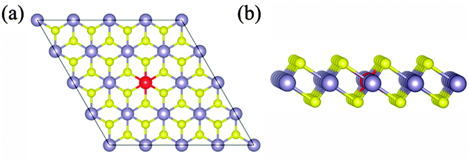
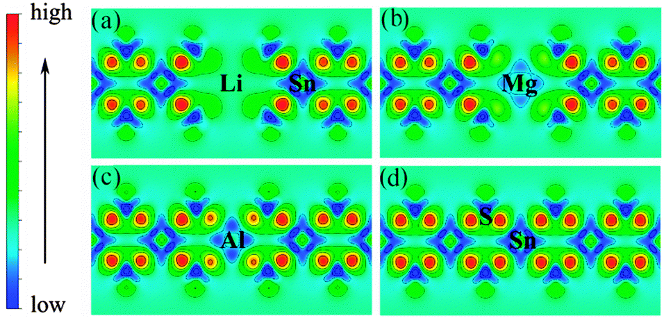
Low valence metal X doping in single-layer SnS2 was modeled by replacing the Sn site with one X atom (X = Li, Mg, and Al) (XSn) in the supercell. The top view and side view of the optimized SnS2 monolayer are shown in Fig. 1. In order to explore the bonding nature in X-doped single-layer SnS2, the difference in charge density near dopant X is simulated and plotted in Fig. 2. For pure single-layer SnS2 (Fig. 2(d)), covalent bonding apparently exists between Sn and S atoms. For X-doped single-layer SnS2, it is easy to find that the covalent character of a X–S bond is gradually weakened while the ionic character is enhanced with the increase in hole density (from Fig. 2(c) to (a)). Furthermore, significant ionic bonding behavior is observed between the Li and adjacent S atoms in Li-doped SnS2. To further understand the chemical bond characteristic, the Bader charge34 was calculated to analyze the charge transfer of every atom and the related X–S bond length is also presented, as summarized in Table 2. Positive and negative values indicate the loss and gain of charge, respectively. As can be seen, the valence electron on the Li atom is almost lost, which shows that an obvious ionic bond character is easy to form in Li-doped SnS2. Besides, the charge transfer rate decreases with the decreasing hole density introduced by the dopant, indicating that the electron transfer becomes increasingly unobvious, thereby resulting in the ionicity being weakened. This is in agreement with the above analysis of the difference in charge density. In addition, the results in Table 2 show that the X–S bond length (X = Li, Mg, and Al) is larger than that of Sn–S in pristine single-layer SnS2. It is well known that covalent bond strength is greater than ionic bond strength. Consequently, a possible reason for the above conclusion is the existence of a strong Sn–S covalent bond relative to a Li(Mg)–S ionic bond and slightly weak Al–S covalent bond. In particular, combining the results shown in Table 2 and Fig. 2, it can be seen that the ionicity of the Li–S bond is much stronger than that of the Mg–S bond, thus leading to a shorter length for the Li–S bond (2.540 Å) than the Mg–S bond (2.567 Å).
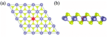 |
| | Fig. 1 The top view (a) and side view (b) of optimized X-doped single-layer SnS2. Yellow, dark and red spheres represent the S, Sn and X (X = Li, Mg and Al) atoms, respectively. | |
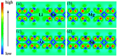 |
| | Fig. 2 Charge density difference near the dopant X and adjacent host atoms for (a) Li-, (b) Mg-, (c) Al-doped SnS2, and (d) pure single-layer SnS2. | |
Table 2 The Bader charge on the dopant X and its adjacent host atoms, as well as the X–S bond length dX–S (Å) are listed
| Bader charge (e) |
| Species |
Sn |
S |
Li |
Mg |
Al |
d
X–S (Å) |
| Li:SnS2 |
1.48 |
−0.67 |
0.84 |
— |
— |
2.540 |
| Mg:SnS2 |
1.48 |
−0.79 |
— |
1.58 |
— |
2.567 |
| Al:SnS2 |
1.48 |
−0.89 |
— |
— |
2.20 |
2.451 |
| Pure |
1.48 |
−0.74 |
— |
— |
— |
2.437 |
In order to check the relative stability of the doped systems, the formation energy of X substitution with charged state q is calculated according to the following formula
| |  | (1) |
where
E(doped) and
E(pure) denote the total energies of X-doped and pure single-layer SnS
2, respectively. The
ni (i = Sn, S and X) is the number of atoms removed (
ni > 0) or added (
ni < 0) to the system, and
μi is the chemical potential of the corresponding species.
EF is the Fermi energy level with respect to the energy position of the valence band maximum (
εVBM) of the perfect single-layer SnS
2. Δ
ν is the correction for the shift in average electron static potential of the 1s core level energy of a Sn atom (located far away from the defect site) between the neutral and charged states. As is well known, the formation energy depends on the growth conditions, which may be either Sn-rich or S-rich conditions. Conventionally,
μi =
μbulki +Δ
μi, where
μbulki is defined as the chemical potential of the elemental bulk solid, and Δ
μi denotes the chemical potential change of defects under different growth conditions. To avoid the precipitation of SnS or Sn
2S
3 in the SnS
2 phase, we set constraints on the chemical potentials of the type
mΔ
μSn +
nΔ
μS ≤ Δ
H(Sn
mS
n),
35 in which Δ
H(Sn
mS
n) is the formation enthalpy of Sn
mS
n, and we obtain −3.54 eV ≤ Δ
μSn ≤ −0.06 eV from the constraints. The value Δ
μSn = −0.06 eV corresponds to the Sn-rich environment, whereas Δ
μSn = −3.54 eV characterizes the Sn-poor (S-rich) condition. Then
μS is computed using the equilibrium condition in SnS
2:
μSn + 2
μS =
μSnS2. In addition, during the metal element X doping process, the restriction
mΔ
μX +
nΔ
μS ≤ Δ
H(X
mS
n) is further considered to prevent the formation of phases Li
2S, MgS, and Al
2S
3 between the dopant and host atoms. According to
eqn (1), the neutral formation energies of X doping in single-layer SnS
2 are calculated under different conditions, as summarized in
Table 3. The results show that the formation energies are lower under S-rich conditions than those under Sn-rich conditions for all doping cases, which implies that the doping is energetically favored under S-rich conditions. In particular, there exists the lowest formation energy (
Ef) when the Sn site is substituted by an Al atom, which shows that Al doping is easier to achieve compared with Li and Mg doping. Besides, the
Ef shows a decreasing trend with the decreasing hole density. The values of
Ef are in the order Li > Mg > Al, which is consistent with the order of ionic radius (Li > Mg > Al) but not in agreement with that of electronegativity (Li (0.98) < Mg (1.31) < Al (1.61)). This indicates that the influence of the ionic radius on the
Ef exceeds the electronegativity so that suitable ion size plays a significant role in the feasibility of doping in single-layer SnS
2 in experiments. Meanwhile, to investigate the transition energy level between the neutral and charged defects, the formation energies of a X-doped SnS
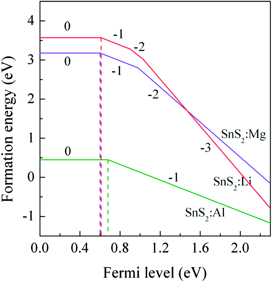
2 monolayer in different charged states under S-rich growth conditions were calculated.
Fig. 3 shows the formation energies as a function of the Fermi level
EF. It can be seen that the calculated (0/−1) transition energy levels are 0.61 eV, 0.60 eV and 0.68 eV above the VBM for Li, Mg and Al-doped single-layer SnS
2, respectively. These large values of transition energy level indicate that the X dopants are deep acceptor impurities.
Table 3 The total magnetic moments M (μB), and formation energies Ef (eV) of X-doped single-layer SnS2 under Sn-rich and S-rich conditions
| X-doped SnS2 |
M (μB) |
E
f (eV) |
| Sn-rich |
S-rich |
| Li |
3.00 |
5.18 |
3.57 |
| Mg |
1.75 |
4.92 |
3.18 |
| Al |
0 |
1.32 |
0.45 |
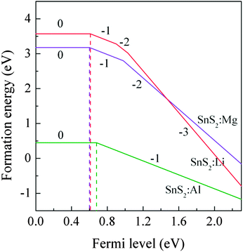 |
| | Fig. 3 The formation energies of X substitution (XSn) as a function of the Fermi level under S-rich conditions. | |
On the other hand, another issue that should be paid attention is the formation of compensating defects, which can kill the hole carriers, for instance the formation of a S vacancy (VS). This hole killing mechanism has been already observed in the DFT+U studies of Cu-doped ZnS reported by Wang et al.36 Therefore, the complex defect of XSn + VS is introduced to explore whether it is more favorable or challenging to form p-type characteristics in the X-doped SnS2 monolayer. Based on our calculations, the formation energies of the complex defect of XSn + VS under S-rich conditions are 12.15 eV, 8.38 eV and 5.06 eV for Li, Mg and Al-doped SnS2, respectively, which are much higher than that of separated neutral and charged XSn and VS defects. It indicates that the VS related defects are difficult to form in this situation. That is to say, this mechanism of hole compensation could be less pronounced in eliminating the hole carriers, thereby making the p-type doping for SnS2 more favorable.
3.2. Electronic properties
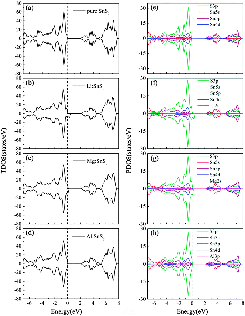
To investigate the effects of doping on the characteristics of the electronic structure of SnS2, we present the total density of states (TDOS) and partial density of states (PDOS) of single-layer SnS2 with X doping in Fig. 4. For comparison, the TDOS and PDOS of a pure SnS2 monolayer are also calculated and displayed in Fig. 4(a) and (e). As can be seen, for pristine single-layer SnS2, the valence band (VB) mostly comprises the S 3p states, while the conduction band (CB) is mainly dominated by the hybridization of the S 3p and Sn 5s states. These results are in accordance with previous experimental and theoretical calculations,22,26,33 which further indicates our calculated method is reasonable.
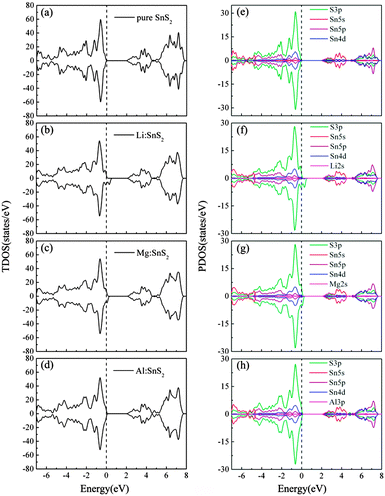 |
| | Fig. 4 Calculated TDOS (a)–(d) and PDOS (e)–(h) for pure and X-doped single-layer SnS2. The vertical dash line indicates the EF position. | |
For Li and Mg doping in single-layer SnS2, as shown in Fig. 4(b) and (c), the Fermi level (EF) penetrates into the VB which indicates p-type doping. The remarkable difference compared to the TDOS in Fig. 4(a) is that the incorporation of Li or Mg atoms leads to the occurrence of defect states located above the valence band maximum (VBM). In addition, the PDOS of Fig. 4(f) and (g) show that the VB is still mainly dominated by the S 3p states and the CB is composed of a mixture of the S 3p and Sn 5s states. The Li or Mg dopant has only a little contribution to the constitution of the VB and CB, but it has a major influence on the adjacent atoms and changes their density of states distribution, thereby resulting in the hybridization between most of the S 3p orbitals and a small number of the Sn 4d orbitals to form the defect states. These defect states are spin-polarized hole states, which makes the spin-up and spin-down TDOS asymmetric and causes spin splitting. This implies that the single-layer SnS2 doped with Li or Mg atoms exhibits magnetic ground states. Fig. 4(d) and (h) present the TDOS and PDOS of Al doping in single-layer SnS2. Similar to the Li and Mg doping cases, the components of the VB and CB show no obvious changes, and the injection of Al atoms also introduces defect states with S 3p orbital character in the band gap. However, one can see that the spin-up and spin-down TDOS are symmetric, which suggests that the Al-doped single-layer SnS2 exhibits non-magnetic ground states.
Table 3 lists the calculated total magnetic moments of doped systems. They are 3.00 μB, 1.75 μB and 0 μB for Li, Mg and Al doped SnS2, respectively. We notice that the induced magnetic moments exhibit a monotonic decreasing trend, which may be ascribed to the decrease in hole density introduced by doping. In particular, although one hole is injected when the Al substitutes a Sn atom, the system is non-spin-polarized. The reason can be explained as follows; it is well known that the hole-doped system becomes spin polarized if it satisfies the Stoner criterion D(EF)J > 1, where D(EF) is the density of states at the Fermi level and J denotes the strength of the exchange interaction.27 As can be seen from the TDOS, the values of D(EF) are 8.94, 7.55 and 0.79 states per eV for Li, Mg, and Al doping, respectively. This value for Al doping is relatively small compared to that for Li and Mg doping. Consequently, the relatively low D (EF) will result in the Stoner criterion being unlikely to be satisfied and thereby there is no magnetic moment in Al-doped single-layer SnS2. In order to more intuitively observe the distribution of magnetic moments, the spin density distributions of Li and Mg doped systems are plotted in Fig. 5. Obviously, the spin density is mainly located on the nearest-neighbor and third-neighbor S atoms. The dopant Li or Mg has no spin polarization, which differs from the results of nonmetal doping in the SnS2 monolayer,26 in which the induced spin polarizations are almost located on the defect site. The above results suggest that the only key role of the dopant is to provide S atoms with holes and the spontaneous magnetization in the system is induced by the hole with S 3p orbital character, which is consistent with the analysis of the density of states.
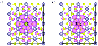 |
| | Fig. 5 Spin density distribution for Li-doped (a) and Mg-doped (b) single-layer SnS2. | |
3.3. Optical properties and photochemical energy conversion applications
As a promising material in the fields of photovoltaic devices and photocatalysis, it is essential to explore the effects of X doping on the optical properties of single-layer SnS2. In our calculations, the optical absorption coefficient α(ω) is obtained from the expression:| |  | (2) |
where the imaginary part ε2(ω) is directly associated with optical absorption and the real part ε1(ω) is calculated from ε2(ω) by the Kramer–Kronig transformation:37| | 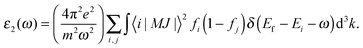 | (3) |
In Fig. 6, we present the optical absorption spectra of X-doped single-layer SnS2 as a function of photon energy. As a reference, the optical absorption coefficient of pure SnS2 monolayer is also calculated and plotted in Fig. 6. Moreover, different optical incident light polarization directions, parallel (E∥z) and perpendicular (E⊥z) to the z-axis, are taken into account in this work for each doping case. As can be seen from Fig. 6, the characteristics of the optical absorption coefficients along the E∥z and E⊥z directions are different, which indicates that the optical absorption presents anisotropy for doped systems. This is owing to the different dielectric response caused by the hexagonal structure of doped SnS2. The optical anisotropy is also observed in Sn1−xTixS2 ternary alloys.31 Besides, for all doping cases, the absorption along the E⊥z direction is stronger than that along the E∥z direction. Thus, in order to enhance the efficiency of the solar spectrum, the growth direction perpendicular to the z-axis should be chosen for the low valence metal X-doped single-layer SnS2. In Fig. 6(a), we can see that the absorption edges of the three doped systems exhibit an obvious red shift with respect to pure SnS2, which is associated with the decrease in band gap. It indicates that low valence metal X doping is beneficial to improve the optical absorption in the visible light range. Furthermore, a broad absorbance peak from 0 to 2 eV occurs for each doping case, which is advantageous to improve the capacity of absorption in the low energy region. From the density of states analysis in Section 3.2, the appearance of the peak is directly related to the intraband transition caused by the unoccupied S 3p states located above the EF. That is to say, the low valence metal X doping in single-layer SnS2 can enhance the effective utilization of the solar spectrum, especially in the near-infrared light region.
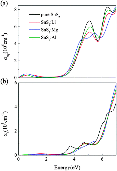 |
| | Fig. 6 The optical absorption coefficients as a function of photon energy along the directions of perpendicular (a) and parallel (b) to the z axis for X doping in single-layer SnS2. | |
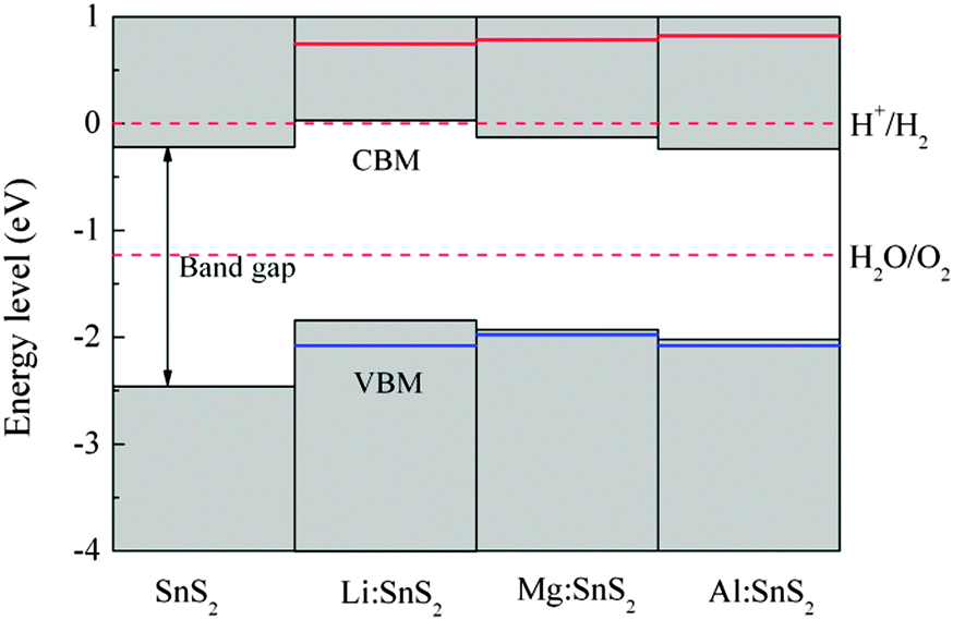
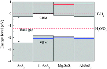
In order to evaluate the effects of X-doped SnS2 on photocatalytic water splitting, the energy levels of the doped systems are calculated and compared with the standard reduction and oxidation potentials of water. In our work, the energy zero is set to the reduction potential of H+/H2, and the valence and conduction band-edge positions are estimated from the calculated density of states. As a reference, the energy level diagram of pure single-layer SnS2 is also given in Fig. 7. Apparently, the VBM of the pristine SnS2 monolayer is below the oxidation potential of H2O/O2 while the CBM does not lie across the reduction potential of H+/H2. This indicates that pure single-layer SnS2 is only favorable for oxygen evolution but not for hydrogen evolution, which agrees with the theoretical results of ref. 24. For X-doped (Mg and Al) single-layer SnS2, the values of the VBM lie more negative than the oxidation level of water and the CBM values still lie within the reduction level of water, which shows that they are active only for the photo-oxidation of water. However, for Li doping in SnS2, the VBM lie more negative than the oxidation potential of H2O/O2 and the CBM is about 0.03 eV higher than the reduction potential of H+/H2, which indicates that the doped system is beneficial for both the photo-reduction and photo-oxidation of water. Furthermore, the stability of semiconductors in aqueous solution is also important for the photocatalytic ability of materials, in addition to the band edge alignment. As reported by Wang et al.,38 whether the semiconductor is resistant to photocorrosion depends on the alignment of thermodynamic oxidation (φox) and reduction potentials (φre) relative to the water redox potentials. The φox and φre should be taken into account for the choice of candidate photocatalytic materials. Therefore, in order to investigate the stability of doped systems in aqueous solution, the thermodynamic potentials were estimated with the model proposed by Wang et al., as shown in Fig. 7. As can be seen, the φox is lower than the oxidation potential of H2O/O2 for Mg (or Al)-doped single-layer SnS2, which shows that this material is stable with respect to hole oxidation. For Li-doped SnS2, the φox is lower than the oxidation potential of H2O/O2 and the φre is higher than the reduction potential of H+/H2, indicating this doped system is stable with respect to both hole oxidation and electron reduction. Thus, Li-doped single-layer SnS2 is expected to be a potential candidate for overall water splitting under visible light radiation.
 |
| | Fig. 7 Energy level diagram of pure and X-doped single-layer SnS2 with respect to the standard reduction and oxidation potentials of water. The red and blue solid lines indicate the thermodynamic reduction and oxidation potentials, respectively. | |
4. Conclusions
The first-principles calculations were performed to investigate the electronic and optical properties of low valence metal X (X = Li, Mg and Al) doping in single-layer SnS2. The results show that the doping is energetically favored under S-rich conditions with respect to Sn-rich conditions, and Al doping is easier to realize than Li and Mg doping. There is ionic bonding character for Li–S and Mg–S bonds, and covalent bonding behavior for Al–S bonds. The defect states of S 3p character are introduced in the band gap, leading to a total magnetic moment of 3.00 μB and 1.75 μB for Li and Mg-doped SnS2, respectively. However, the system with Al doping exhibits non-magnetic ground states, which is due to the low hole density around the Fermi level. The calculations of optical properties show that the optical absorption along the xy plane is stronger than that along the z direction, and the red shift of absorption edges is observed for all doping cases, which accordingly improves the photocatalytic ability in the visible light range. Also, the effective utilization in the near-infrared light region is enhanced because of the defect states. In addition, Li-doped single-layer SnS2 is expected to be a potential candidate for overall water splitting whereas Mg and Al doping is suitable only for oxygen evolution.
Acknowledgements
This work was supported by the National Natural Science Foundation of China (51074112) and (11247224), and the supercomputing resources were supported by the High Performance Computing Center of Tianjin University, China.
References
- K. S. Novoselov, A. K. Geim, S. V. Morozov, D. Jiang, Y. Zhang, S. V. Dubonos, I. V. Grigorieva and A. A. Firsov, Science, 2004, 306, 666–669 CrossRef CAS PubMed.
- P. Avouris, Z. Chen and V. Perebeinos, Nat. Nanotechnol., 2007, 2, 605 CrossRef CAS PubMed.
- A. K. Geim and K. S. Novoselov, Nat. Mater., 2007, 6, 183 CrossRef CAS PubMed.
- C. N. R. Rao, K. Biswas, K. S. Subrahmanyam and A. Govindaraj, J. Mater. Chem., 2009, 19, 2457 RSC.
- C. N. R. Rao, A. K. Sood, K. S. Subrahmanyam and A. Govindaraj, Angew. Chem., Int. Ed., 2009, 48, 7752 CrossRef CAS PubMed.
- D. Golberg, Y. Bando, Y. Huang, T. Terao, M. Mitome, C. C. Tang and C. Y. Zhi, ACS Nano, 2010, 4, 2979–2993 CrossRef CAS PubMed.
- A. Pakdel, X. B. Wang, C. Y. Zhi, Y. Bando, K. Watanabe, T. Sekiguchi, T. Nakayama and D. Golberg, J. Mater. Chem., 2012, 22, 4818–4824 RSC.
- C. Xia, Y. Peng, S. Wei and Y. Jia, Acta Mater., 2013, 61, 7720–7725 CrossRef CAS.
- C. H. Ho, M. H. Hsieh and C. C. Wu, Rev. Sci. Instrum., 2006, 77, 113102 CrossRef.
- Y. C. Huang, C. Y. Ling, H. Liu, S. Y. Wang and B. Y. Geng, J. Phys. Chem. C, 2014, 118, 9251–9260 CAS.
- R. Wei, J. Hu, T. Zhou, X. Zhou, J. Liu and J. Li, Acta Mater., 2014, 66, 163–171 CrossRef CAS.
- D. M. Guzman and A. Strachan, J. Appl. Phys., 2014, 115, 243701 CrossRef.
- W. Z. Bao, X. H. Cai, D. Kim, K. Sridhara and M. S. Fuhrer, Appl. Phys. Lett., 2013, 102, 042104 CrossRef.
- Y. Ge, W. Wan, W. Feng, D. Xiao and Y. Yao, Phys. Rev. B: Condens. Matter Mater. Phys., 2014, 90, 035414 CrossRef.
- S. Das, H. Y. Chen, A. V. Penumatcha and J. Appenzeller, Nano Lett., 2013, 13, 100 CrossRef CAS PubMed.
- P. Chen, Y. Su, H. Liu and Y. Wang, ACS Appl. Mater. Interfaces, 2013, 5, 12073–12082 CAS.
- D. Ma, H. Zhou, J. Zhang and Y. Qian, Mater. Chem. Phys., 2008, 111, 391–395 CrossRef CAS.
- Y. C. Zhang, Z. N. Du, S. Y. Li and M. Zhang, Appl. Catal., B, 2010, 95, 153–159 CrossRef CAS.
- J. Yu, C. Y. Xu, F. X. Ma, S. P. Hu, Y. W. Zhang and L. Zhen, ACS Appl. Mater. Interfaces, 2014, 6, 22370–22377 CAS.
- S. H. Chaki, M. P. Deshpande, D. P. Trivedi, J. P. Tailor, M. D. Chaudhary and K. Mahato, Appl. Nanosci., 2013, 3, 189 CrossRef CAS.
- J. Seo, J. Jang, S. Park, C. Kim, B. Park and J. Cheon, Adv. Mater., 2008, 20, 4269 CrossRef CAS.
- Y. Sun, H. Cheng, S. Gao, Z. Sun, Q. Liu, Q. Liu, F. Lei, T. Yao, J. He, S. Wei and Y. Xie, Angew. Chem., Int. Ed., 2012, 51, 8727 CrossRef CAS PubMed.
- R. Wei, J. Hu, T. Zhou, X. Zhou, J. Liu and J. Li, Acta Mater., 2014, 66, 163–171 CrossRef CAS.
- H. L. Zhuang and R. G. Hennig, Phys. Rev. B: Condens. Matter Mater. Phys., 2013, 88, 115314 CrossRef.
- X. An, C. Y. Jimmy and J. Tang, J. Mater. Chem. A, 2014, 2, 1000 CAS.
- C. X. Xia, Y. T. Peng, H. Zhang, T. X. Wang, S. Y. Wei and Y. Jia, Phys. Chem. Chem. Phys., 2014, 16, 19674 RSC.
- H. W. Peng, H. J. Xiang, S. H. Wei, S. S. Li, J. B. Xia and J. B. Li, Phys. Rev. Lett., 2009, 102, 017201 CrossRef PubMed.
- G. Kresse and J. Hafner, Phys. Rev. B: Condens. Matter Mater. Phys., 1993, 47, 558 CrossRef CAS.
- G. Kresse and J. Furthmuller, Phys. Rev. B: Condens. Matter Mater. Phys., 1996, 54, 11169 CrossRef CAS.
- J. P. Perdew, K. Burke and M. Ernzerhof, Phys. Rev. Lett., 1996, 77, 3865–3868 CrossRef CAS PubMed.
- C. Xia, J. An, T. Wang, S. Wei and Y. Jia, Acta Mater., 2014, 72, 223–228 CrossRef CAS.
- S. Grimme, J. Comput. Chem., 2006, 85, 1787–1799 CrossRef PubMed.
- S. K. Arora, D. H. Patel and M. K. Agarwal, Cryst. Res. Technol., 1993, 28, 623–627 CrossRef CAS.
-
R. F. W. Bader, Atoms in Molecules: a Quantum Theory, Oxford University Press, New York, 1990 Search PubMed.
- B. D. Malone, A. Gali and E. Kaxiras, Phys. Chem. Chem. Phys., 2014, 16, 26176–26183 RSC.
- H. H. Pham, G. T. Barkema and L.-W. Wang, Phys. Chem. Chem. Phys., 2015, 17, 26270–26276 RSC.
- C. M. I. Okoye, J. Phys.: Condens. Matter, 2003, 15, 5945 CrossRef CAS.
- S. Chen and L.-W. Wang, Chem. Mater., 2012, 24, 3659–3666 CrossRef CAS.
|
| This journal is © the Owner Societies 2016 |
Click here to see how this site uses Cookies. View our privacy policy here.