Synthesis of ZnO nanosheet arrays with exposed (100) facets for gas sensing applications†
Received
17th July 2015
, Accepted 12th November 2015
First published on 13th November 2015
Abstract
ZnO nanosheet (NS) arrays have been synthesized by a facile ultrathin liquid layer electrodeposition method. The ion concentration and electrode potential play important roles in the formation of ZnO NS arrays. Studies on the structural information indicate that the NSs are exposed with (100) facets. The results of Raman and PL spectra indicate that there existed a large amount of oxygen vacancies in the NSs. The gas sensing performances of the ZnO NS arrays are investigated: the ZnO NS arrays exhibited high gas selectivity and quick response/recovery for detecting NO2 at a low working temperature. High binding energies between NO2 molecules and exposed ZnO(100) facets lead to large surface reconstructions, which is responsible for the intrinsic NO2 sensing properties. In addition, the highly exposed surface and a large amount of oxygen vacancies existing in the NSs also make a great contribution to the gas sensing performance.
1 Introduction
Zinc oxide, a promising n-type semiconductor, has been applied in many devices, such as gas sensors, photocatalysts, optoelectronic devices and solar cells.1–4 As one of the competitive candidates for applications in gas sensors due to their advantages of high sensitivity, stability and low-cost, ZnO nano-structures have already been widely used for detecting gases such as CO, NO2, and ethanol.5–10 With the progress of gas-sensing research, it has been found that nanostructures with the high surface area and surface accessibility can significantly improve the gas-sensing properties, and thus plenty of attention has been focused on the preparation of ZnO nanostructures.5 Small size ZnO nanoparticles exhibit excellent gas sensing properties due to their high specific surface area and activity. However, the inevitable aggregation of the nanoparticles hinders the diffusion of gases into the inner part of the secondary particles, which will eventually worsen and delay the response. Recently, 2D ZnO nanostructures such as nanosheets, nanowalls, and nanoplates have attracted particular attention for gas sensing properties because of their high surface to volume ratios and comparable lateral dimensions and the thickness of the surface space-charge region.7,11 The synergic combination of the two effects can make it with high detection efficiencies at low operating temperature, fast response and recovery capability. Thus, the 2D ZnO nanomaterials are widely applied as efficient components of some efficient gas sensors to participate in the detection of various hazardous and toxic gases. Until now, only a few reports have been made for the synthesis of 2D ZnO nanostructures grown by different fabrication techniques.
It is generally recognized that the performances of solid state gas sensors are directly dependent on the surface state and morphology of the sensing materials.12,13 Theoretical and experimental results indicate that nanosized materials can exhibit special features corresponding to their nanostructures encased in specific facets.8,11,14–16 Recently, there has been growing interest in the synthesis of nanostructures with specifically exposed crystal surfaces and in the exploration of their crystal plane-dependent properties for applications such as in gas sensors and catalysts.8,11,12 As is well known, the gas sensing behaviour of metal-oxide semiconductors is mainly dominated by interactions between the target gas and the sensing surface, which brings about a resistance change. Hence, gas sensors exhibit different surface properties (such as defect concentration, surface modification and exposed facets), which could lead to varying gas sensing performance.
Activated by the above-mentioned feature, ZnO NS arrays were prepared by an electrochemical deposition self-assembly approach in a quasi-two-dimensional ultra-thin liquid layer. The single-crystalline ZnO NSs are exposed with (100) facets and there exists some amount of oxygen vacancies. The thickness of NSs is about 20 nm, which is comparable to the Debye length. The as-obtained ZnO NS arrays are developed for the detection of NO2 gas which exhibit high selectivity, short response and recovery time. In addition, the gas-sensing mechanism of such excellent sensing performance is discussed.
2 Experimental
2.1 Synthesis of ZnO NS arrays
All the chemicals were analytical grade reagents without further purification. The electrolyte solution of 0.04 M Zn(NO3)2 was prepared using Millipore water. The growth system consisted of a growth chamber, a low temperature cycle water bath, a DC power supply (DF1731SB5A), an arbitrary function generator (AFG 310), an optical microscope (Leica Dmlm) and a CCD camera (A311f). A Peltier element attached to DC power supply was fixed in the center of the growth chamber, which was used to rapidly adjust the electrolyte temperature. The growth chamber temperature was controlled using a low-temperature cycle water bath, and the growth potential was supplied by an arbitrary function generator. The growth process could be observed using an optical microscope and a CCD camera.
Firstly, silicon substrates (WaterNet Co., Type N, 0.5 mm thick, orientation [100], resistivity 2–5 Ω cm−1) were cut into pieces of about 20 × 20 mm2 before use. And secondly, they were completely cleaned with acetone, chloroform, ethanol, and Millipore water for 10 min, respectively, under the ultrasonic circumstances and then blown dry with high-purity nitrogen. Finally, they were treated with oxygen plasma for 3 min at 300 W (Templa System 100-E plasma system) and rinsed again with Millipore water. The surface of silicon substrates became fully hydrophilic after the above procedure. Surface structures with –CH3 termination were carried out by immersing the silicon substrate into a 1 mm OTS (APTMS, Aldrich) solution of 1-phenyloctane (Aldrich) or hexadecane (Aldrich) for 15 min under the ultrasonic conditions, and then were rinsed in chloroform to remove the polymeric residuals. Subsequently, the silicon wafer was placed on the Peltier element while two parallel electrodes made up of a 30 μm thick Zn foil were put on silicon substrates and separated by a distance of approximately 8 mm. Then the solution was dropped on the silicon substrate. Finally, a cover glass was carefully put on the two electrodes and then filled the space between the cover glass and the silicon substrate with solution. A uniform ultra-thin ice layer could be formed between the silicon substrate and cover glass by adjusting the temperature of the Peltier element and the low-temperature cycle water bath. After an ultra-thin ice layer was formed, we kept the growth chamber temperature constant for 30 min. The ultrathin liquid layer of the concentrated electrolyte was formed between the ice layer and the upper surface of the silicon substrate, as well as the ice layer and the lower surface of cover glass. Electrodeposition was initiated when a constant voltage of 0.8 V was applied on the parallel electrodes. As the growth process ended, a slight increase in temperature was provided by the Peltier element to melt ice. Then the cover glass and the silicon substrate were taken out for cleaning with deionized water and dried at room temperature. The growth process is displayed in the ESI.†
2.2 Characterization and gas-sensing measurements
The morphology and crystal structure of the ZnO NS arrays were characterized using scanning electron microscopy (SEM FEI Magellan-400), X-ray diffraction (XRD, Rigaku D/max-Ra) and transmission electron microscopy (TEM, JEOL JEM-2200FS), respectively. Transmission spectra were recorded on a HR-800 Lab Ram Infinity spectrophotometer which was carried out using a continuous He–Cd laser with the excitation wavelength of 325 nm and a UV-3150 spectrophotometer, respectively. The room temperature Raman spectrum and PL spectrum were recorded on a HR-800 LabRam Infinity spectrophotometer excited by a continuous He–Cd laser with a respective excitation wavelength of 325 nm.
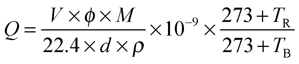
The samples on the cover glass were used as the test objects. At first, the samples were covered by a linear mask with a width of 50 μm. Two copper wires were fixed on both sides of the mask separately. Then the Au film was deposited on the glass by vacuum ion sputtering for 300 s. After that, the mask was taken away, and the NS arrays were connected into the circuit. During the measurement, the electrical signals were measured and recorded using a Keithley 2400 sourcemeter (2400, Keithley, USA) and a Digital Phosphor Oscilloscope (TDS5034B, Tektronix, USA). The working temperature was controlled by a flat heating plate with a temperature controller. The desired concentrations of the testing gases were obtained by the static gas distribution method, which was calculated by the following formula:5
| |  | (1) |
where
Q (mL) is the liquid volume of the volatile compound or gas volume;
V (mL) is the volume of the testing chamber;
φ (ppm) is the required gas volume fraction;
M (g mol
−1) is the molecular molar mass;
d (g cm
−3) is the specific gravity, and
ρ is the purity of the volatile testing liquid or gas;
TR and
TB (°C) are the temperatures at ambient and the test chamber, respectively. The sensor response (
R) is defined as the relative conductance (resistance) variation upon exposure to reducing (oxidizing) target gases, respectively.
3 The gas sensing measurements are carried out at a relative humidity (RH) of 30% at 25 °C. The response time is defined as the time taken by a sensor to reach 90% of its saturation value after it is exposed to detect gases, and the recovery time is the time for recovery of the resistance to 90% of the initial level after exposure to air. The uncertainty of the gas sensing test is mainly induced by the electrode connection process.
3 Results and discussion
3.1 Structure, morphology and optical properties
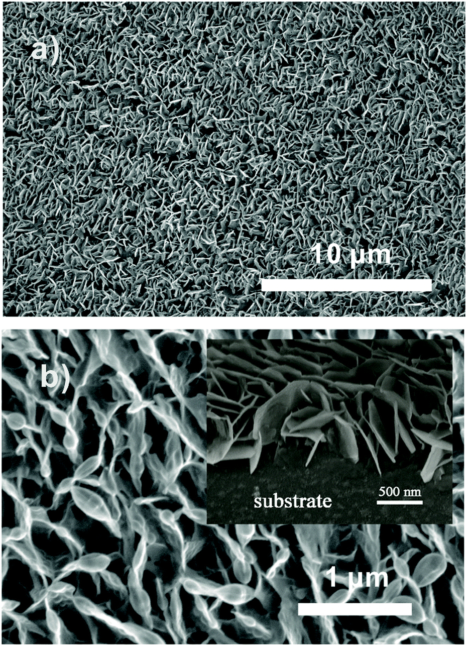
Fig. 1a and b display the SEM images of ZnO NS arrays with low and high magnification, and the inset image (in Fig. 1b) displays the cross-sectional view of the NS arrays. The images illustrate that the ZnO array is interwoven by abundant NSs with an average thickness of 20 nm. The unique NS arrays with external inter-space between each NS can provide an extensive pore network for gas diffusion.
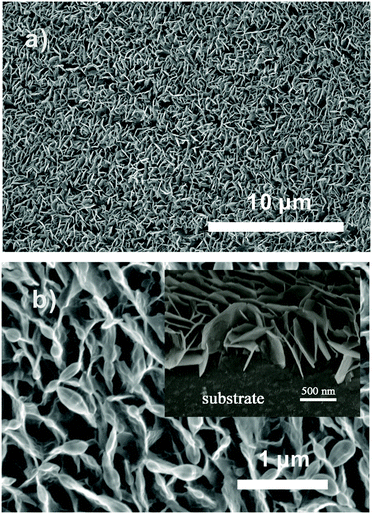 |
| | Fig. 1 (a) Low- and (b) high-magnification SEM images of ZnO NS arrays. The inset is the cross-sectional view of the NS arrays. | |
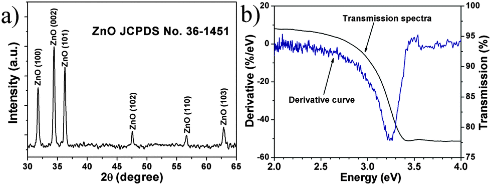
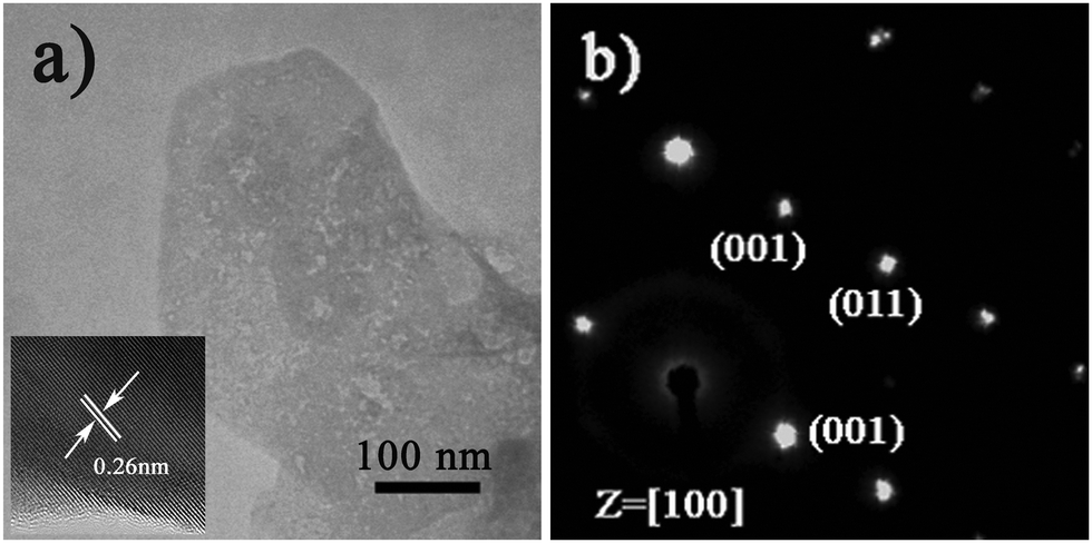
To gain the component and structural information of ZnO NS arrays, XRD, TEM and spectrum experiments were conducted. The XRD pattern of ZnO NS arrays is shown in Fig. 2a. All the diffraction peaks match to those characteristic of the wurtzite ZnO structure (JCPDS 036-1451). No characteristic peaks of other chemical compounds were observed such as Zn or Zn(OH)2, indicating that the electrodeposition product is pure ZnO. Fig. 2b depicts the transmission spectrum and its derivative curve of the ZnO NS arrays. Only one distinct peak is observed at about 3.24 eV in derivative curves, which arises from the ZnO near-band-edge (NBE) absorption. Further structural characterization of the as-synthesized nanodeposits was performed using TEM. Fig. 3a shows a TEM image of the individual ZnO NS. The HR-TEM analysis of an individual NS (the inset of Fig. 3a) reveals that clear lattice fringes with a lattice spacing of 0.26 nm correspond well to the d-spacing of the (002) plane of the hexagonal wurtzite ZnO. The selected area electron diffraction (SAED) pattern of the ZnO NSs shown in Fig. 3b can be indexed to the (100) zone axis of single crystal hexagonal wurtzite ZnO. On the basis of the above observations and structural analysis, we can conclude that the exposed surfaces of the as-prepared ZnO NSs are (100) facets.
 |
| | Fig. 2 (a) XRD pattern of ZnO NS arrays. (b) Transmission spectra (black line) and the corresponding derivative curves (blue line) of ZnO NS arrays. | |
 |
| | Fig. 3 (a) TEM and (b) SEAD images of the individual ZnO NS. The inset shows the corresponding HR-TEM pattern. | |
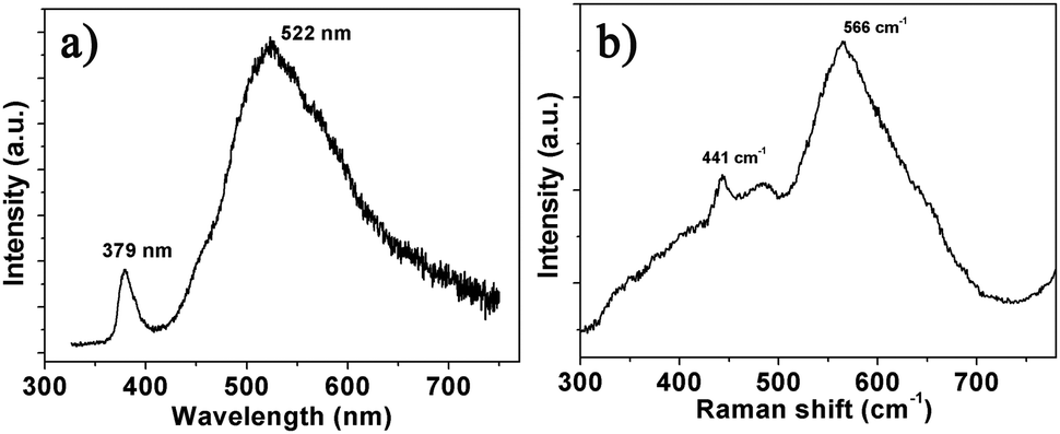
The gas-sensing mechanism of semiconductor gas sensors is generally based on the adsorption and reaction of gas molecules on the material surface, where oxygen deficiency plays an important role. Usually, the Raman and PL spectra are obtained to analyse the defects of semiconductor materials due to their higher sensitivity to crystal imperfections. Fig. 4a displays the typical PL spectrum indicating two bands at 379 and 522 nm. The ultraviolet (UV) peak near 380 nm can be attributed to the conduction band to valence band (CB–VB) combination according to the result of the transmission spectrum in Fig. 2b. The green PL near 500 nm is usually ascribed to oxygen vacancies and the yellow or orange PL (near 600 nm) is related to oxygen interstitials.17 Two peaks of the Raman spectrum at 441 and 566 cm−1 shown in Fig. 4b are assigned to the E2H, and E1L vibrational modes of ZnO, respectively. The E2H mode involves oxygen atoms, and the E1L mode is associated with oxygen deficiency indicating that oxygen vacancies exist in the NSs.18 The broad features of the 566 cm−1 peak in the Raman spectra and the high intensity 500 nm band in the PL spectrum indicate that ZnO NSs are significantly deficient in oxygen.17,18 According to the above analyses, there exists large amounts of oxygen vacancies in the ZnO NS arrays.
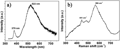 |
| | Fig. 4 (a) PL and (b) Raman spectra of the ZnO NS arrays. | |
3.2 Gas-sensing properties
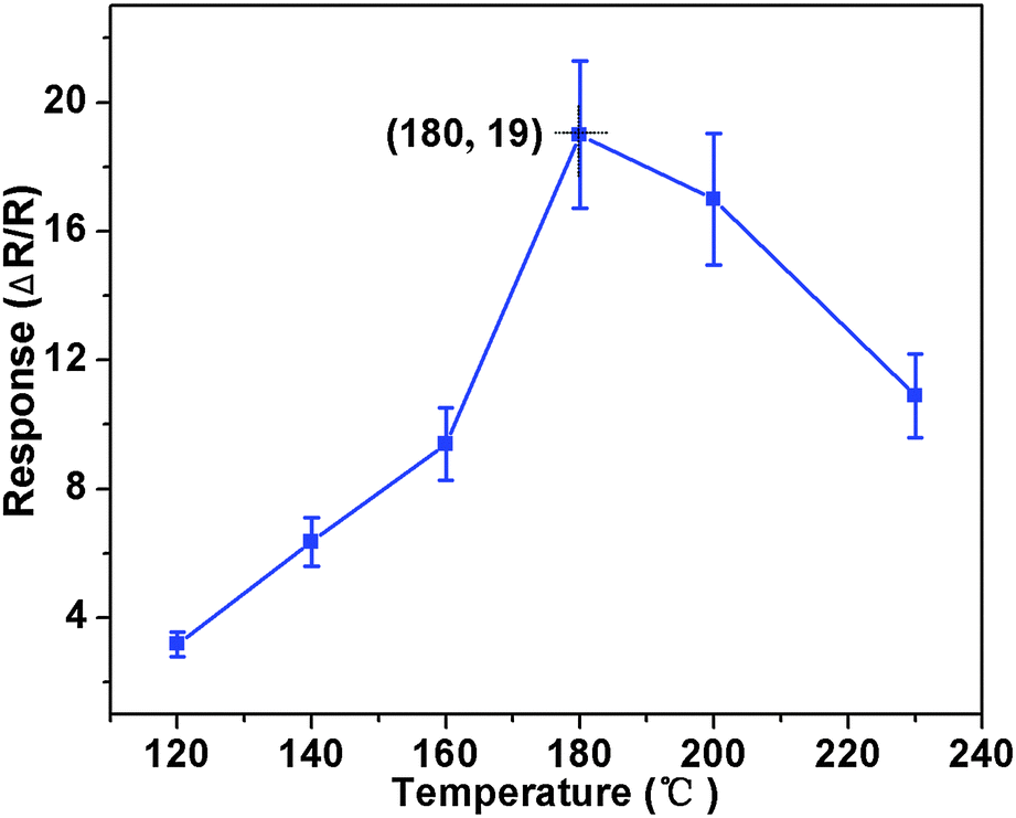
Based on the as-prepared ZnO NS arrays, we fabricate chemical sensors and investigate their gas sensing performances. The gas-sensing properties are heavily affected by the working temperature, as this factor greatly influences the surface state of sensing materials. Therefore, in order to investigate the influence of the operating temperature and to find an optimum operating temperature of the sensors, the sensitivities of the as-prepared ZnO nanostructures toward 100 ppm of NO2 as a function of working temperature are tested and the results are shown in Fig. 5. It can be observed that the sensitivity of the ZnO NS sensor increases gradually while the working temperature rises from 120 to 180 °C and reaches a maximum value of R = 20 at 180 °C. A further increase of the operating temperature above 180 °C, however, results in a gradual decline in the sensitivity of the sensors. Thus, the operating temperature of 180 °C is the optimal temperature for NO2 detection, so it is chosen as the working temperature to further examine the characteristics of the sensor. Compared with the NO2-sensing properties of other ZnO-based nanostructures,19–22 the sensor in this work exhibits lower or comparable working temperature.
 |
| | Fig. 5 Gas response of ZnO NS arrays to 100 ppm NO2 as a function of the operating temperatures. | |
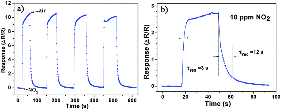
Besides, we further examine other gas-sensing properties including selectivity, detection limit, stability, response and recovery time, which are important parameters for the gas sensor in practical applications. Fig. 6 shows the selectivity of the ZnO NS sensors to NO2 relative to H2S, ethanol, benzene, acetone, methanol, methanal, toluene and NH3 at the same gas concentrations (100 ppm). The gas sensing response to NO2 is much higher than other gases, suggesting that the obtained ZnO NS arrays have high selectivity for NO2. Fig. 7a illustrates that the responses of the sensor are based on ZnO NSs as a function of NO2 concentration from 1 to 400 ppm. In the low concentration range from 1 to 100 ppm, we observe that the sensitivity is approximately linearly increasing with increasing NO2 concentration (shown in the inset of Fig. 7a). Above 100 ppm, the sensitivity changes slowly with the variations of the NO2 concentration, which indicates that the sensor is near saturation. Furthermore, the stability of the gas sensors is also a crucial point for the practical application of the gas sensors. Fig. 7b depicts the representative dynamic responses to different NO2 concentrations (1–400 ppm) at 180 °C, respectively. The response transient of the ZnO NS sensor to 50 ppm NO2 is shown in Fig. 8a. The four sequential cycles of response transients show a reversible, repeatable and stable characteristic. The transient response of ZnO NSs to 10 ppm NO2 is shown in the inset of Fig. 8b. The results indicate that the sensor responds immediately when NO2 gas is introduced and then rapidly recovers to the initial value after the release of NO2. The respective response and recovery time of ZnO NS sensors are around 3 and 12 s. Compared with the NO2 sensing properties of other ZnO-based nanosystems,19–24 the sensor in this work exhibits comparable or wider detection limits but faster response and recovery time, which is due to the specific structure of these ZnO NSs with a greater surface area and highly exposed surface.
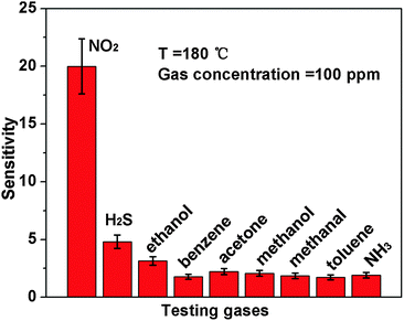 |
| | Fig. 6 Responses of ZnO NS arrays to 100 ppm various testing gases. | |
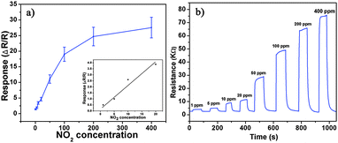 |
| | Fig. 7 (a) Response of ZnO NS arrays to different NO2 concentration. (b) Typical dynamical response of ZnO NS arrays upon exposure to square concentration pulses of NO2. | |
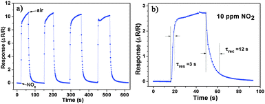 |
| | Fig. 8 (a) Dynamic responses to NO2 of the sensors to NO2 (50 ppm). (b) The response transient of the ZnO based sensors to 10 ppm NO2 at 180 °C. | |
3.3 NO2-sensing mechanism
It is crucial to understand the sensing mechanism for designing NO2 sensors of high sensing performances. As metal oxide ZnO is exposed to air, oxygen molecules will be adsorbed on the oxide surface and then extract electrons in the bulk, leading to a narrow conduction channel. When the n-type semiconductor ZnO is exposed to NO2 gas the NO2 molecules can not only capture electrons from the ZnO conduction band but also react with the chemisorbed oxygen on the surface, which results in withdrawing of electrons from the surface, depleting them from the conduction band, and leading to an increase in resistance (eqn (2) and (3)). When the semiconductor oxide is exposed to air again, NO2− reacts with holes and releases electrons into the conduction band, leading to the release of NO2 into air and reduced resistance (eqn (4)). The adsorption and desorption occur on the ZnO surface according to the following chemical reaction:6| | | NO2(gas) + e− → NO2−(ads) | (2) |
| | | NO2(gas) + O2−(ads) + 2e− → NO2−(ads) + 2O−(ads) | (3) |
| | | NO2−(ads) + h+ → NO2(gas) | (4) |
The kinetics process of gas adsorption and desorption can be understood as follows: when the NO2 gas flows through the sensor element, the adsorption speed of NO2 on the sensor surface is very fast, indicated by the steep slope of the response process. This suggests that the adsorption process plays a dominant role during the initial sensing stage. As the sensing process goes on, the adsorption of the NO2 gas slows down gradually. When the gas adsorption and desorption reach equilibrium, the resistance increases to the maximum value. In contrast, desorption of NO2 gas dominates the sensing process when the NO2 flow is stopped, resulting in the return of the sensor signal to the baseline.
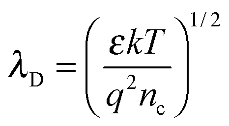
The electron exchange between the surface states and the bulk takes place within a surface layer whose width is about λD (Debye length). The value of λD can be calculated by the following equation:25
| |  | (5) |
where
ε is the static dielectric constant; κ is the Boltzmann constant;
T is the absolute temperature;
q is the electrical charge of the carrier and
nc is the carrier concentration. For bulk ZnO,
λD is about 20 nm at 180 °C according to the above equation as
nc is assumed to be 5 × 10
16 cm
−3. Thus, the thickness of the ZnO NSs is comparable to the Debye length which could effectively enhance the gas sensing performance. It is recognized that the reaction of NO
2 on gas sensing materials is expected to occur mainly
via electron transfer and variation of oxygen species on the surface. Consider that the electrical properties of the semiconductor oxides are significantly influenced by the native defects or the nonstoichiometry. Chemisorbed NO
2 binds more strongly to the oxygen vacancy site, which exists on the ZnO(100) surface, with higher binding energies greater than the clean stoichiometric ZnO(100) surface. Large surface reconstructions around the oxygen vacancy site can take place after NO
2 adsorption, which can lead to large electrical resistance variation.
26 On the other hand, such a rapid sensing performance can be ascribed to be the special NS array structure in which the gas adsorption and desorption would be remarkably improved by the highly exposed internal spaces among the NSs. Meanwhile, most of the active sites in the sensing layer consist of ZnO NSs that can be effectively utilized for contact reactions, resulting in remarkably improved response, lower working temperature and shorter response and recovery time.
4 Conclusions
The hierarchical ZnO arrays assembled from 2D NSs with exposed (100) facets are synthesized through a facile ultrathin liquid layer electrodeposition method. The gas-sensing results reveal that the NS-assembled ZnO arrays exhibit excellent NO2 gas sensing performance evidenced by high response, small cross sensitivity, fast response/recovery (3 s and 12 s) and low operating temperature (180 °C), suggesting their potential applications as advanced gas sensing materials. The excellent performance in sensing can be attributed to the specific morphology of the NS arrays and the thin NSs exposed with (100) facets. In addition, there exists some amount of oxygen vacancies in ZnO NSs which is beneficial for their gas sensing performance. The present work will provide a deeper understanding of the sensing mechanism of ZnO-based sensors, and motivates us to further fabricate other nanomaterials with specifically exposed crystal surfaces for promising applications in gas sensors, photocatalysts and more.
Acknowledgements
This work was funded by the National Science Foundation of China, No. 11174103 and 11474124, and the Graduate Innovation Fund of Jilin University, No. 2015132.
Notes and references
- D. Barreca, D. Bekermann, A. Devi, R. A. Fischer, A. Gasparotto, C. Maccato, E. Tondello, M. Rossi, S. Orlanducci and M. L. Terranova, Chem. Phys. Lett., 2010, 500, 287–290 CrossRef CAS.
- D. Barreca, D. Bekermann, E. Comini, A. Devi, R. A. Fischer, A. Gasparotto, C. Maccato, G. Sberveglieri and E. Tondello, Sens. Actuators, B, 2010, 149, 1–7 CrossRef CAS.
- D. Barreca, D. Bekermann, E. Comini, A. Devi, R. A. Fischer, A. Gasparotto, C. Maccato, C. Sada, G. Sberveglieri and E. Tondello, CrystEngComm, 2010, 12, 3419–3421 RSC.
- L. Schmidt-Mende and J. L. MacManus-Driscoll, Mater. Today, 2007, 10, 40–48 CrossRef CAS.
- Y. Zeng, L. Qiao, Y. Bing, M. Wen, B. Zou, W. Zheng, T. Zhang and G. Zou, Sens. Actuators, B, 2012, 173, 897–902 CrossRef CAS.
- R. Kumar, O. Al-Dossary, G. Kumar and A. Umar, Nano-Micro Lett., 2015, 7, 97–120 CrossRef.
- F. Fan, P. Tang, Y. Wang, Y. Feng, A. Chen, R. Luo and D. Li, Sens. Actuators, B, 2015, 215, 231–240 CrossRef CAS.
- J. Liu, X. Chen, W. Wang, Y. Liu, Q. Huang and Z. Guo, CrystEngComm, 2011, 13, 3425–3431 RSC.
- V. Saxena, D. K. Aswal, M. Kaur, S. P. Koiry, S. K. Gupta, J. V. Yakhmi, R. J. Kshirsagar and S. K. Deshpande, Appl. Phys. Lett., 2007, 90, 043516 CrossRef.
- C. W. Na, H.-S. Woo, I.-D. Kimb and J.-H. Lee, Chem. Commun., 2011, 47, 5148–5150 RSC.
- Y. Xiao, L. Lu, A. Zhang, Y. Zhang, L. Sun, L. Huo and F. Li, ACS Appl. Mater. Interfaces, 2012, 4, 3797–3804 CAS.
- S. Bai, K. Zhang, L. Wang, J. Sun, R. Luo, D. Li and A. Chen, J. Mater. Chem. A, 2014, 2, 7927–7934 CAS.
- Y. V. Kaneti, Z. Zhang, J. Yue, Q. M. Zakaria, C. Chen, X. Jiang and A. Yu, Phys. Chem. Chem. Phys., 2014, 16, 11471–11480 RSC.
- Z. Lai, F. Peng, H. Wang, H. Yu, S. Zhang and H. Zhao, J. Mater. Chem. A, 2013, 1, 4182–4185 CAS.
- X. Han, M. Jin, S. Xie, Q. Kuang, Z. Jiang, Y. Jiang, Z. Xie and L. Zheng, Angew. Chem., 2009, 121, 9344–9347 CrossRef.
- G. Cui, Z. Li, L. Gao and M. Zhang, Phys. Chem. Chem. Phys., 2012, 14, 16321–16325 RSC.
- K. K. Naik, R. Khare, D. Chakravarty, M. A. More, R. Thapa, D. J. Late and C. S. Rout, Appl. Phys. Lett., 2014, 105, 233101 CrossRef.
- D. Li, Y. H. Leung, A. B. Djuriić, Z. T. Liu, M. H. Xie, S. L. Shi and S. J. Xu, and W. K. Chan, Appl. Phys. Lett., 2004, 85, 1601–1603 CrossRef CAS.
- J. H. Jun, J. Yun, K. Cho, I.-S. Hwang, J.-H. Lee and S. Kim, Sens. Actuators, B, 2009, 140, 412–417 CrossRef CAS.
- D. Calestani, M. Villani, R. Mosca, L. Lazzarini, N. Coppedè, S. C. Dhanabalan and A. Zappettini, Nanotechnology, 2014, 25, 365502 CrossRef CAS PubMed.
- L. Shi, A. J. T. Naik, J. B. M. Goodall, C. Tighe, R. Gruar, R. Binions, I. Parkin and J. Darr, Langmuir, 2013, 29, 10603–10609 CrossRef CAS PubMed.
- F. Fan, Y. Feng, S. Bai, J. Feng, A. Chen and D. Li, Sens. Actuators, B, 2013, 185, 377–382 CrossRef CAS.
- F.-T. Liu, S.-F. Gao, S.-K. Pei, S.-C. Tseng and C.-H. J. Liu, J. Taiwan Inst. Chem. Eng., 2009, 40, 528–532 CrossRef CAS.
- J. X. Wang, X. W. Sun, Y. Yang and C. M. L. Wu, Nanotechnology, 2009, 20, 465501 CrossRef CAS PubMed.
- C. L. Zhu, Y. J. Chen, R. X. Wang, L. J. Wang, M. S. Cao and X. L. Shi, Sens. Actuators, B, 2009, 140, 185–189 CrossRef CAS.
- M. Breedon, M. J. S. Spencer and I. Yarovsky, J. Phys. Chem. C, 2010, 114, 16603–16610 CAS.
Footnote |
| † Electronic supplementary information (ESI) available. See DOI: 10.1039/c5cp04183j |
|
| This journal is © the Owner Societies 2016 |
Click here to see how this site uses Cookies. View our privacy policy here.