
Uniform growth of SiC single crystal thin films via a metal–Si alloy flux by vapour–liquid–solid pulsed laser deposition: the possible existence of a precursor liquid flux film
Aomi
Onuma
a,
Shingo
Maruyama
 a,
Takeshi
Mitani
b,
Tomohisa
Kato
b,
Hajime
Okumura
b and
Yuji
Matsumoto
*a
a,
Takeshi
Mitani
b,
Tomohisa
Kato
b,
Hajime
Okumura
b and
Yuji
Matsumoto
*a
aDepartment of Applied Chemistry, Tohoku University, 6-6-07 Aoba, Aramaki, Aoba-ku, Miyagi 980-8579, Japan. E-mail: matsumoto@atomol.che.tohoku.ac.jp
bNational Institute of Advanced Industrial Science and Technology, Onogawa, Tsukuba, Ibaraki 305-8569, Japan
First published on 11th November 2015
Abstract
For their use as next generation power semiconductors, new vapor growth processes for SiC single crystal films have been highly demanded, among which is the vapor–liquid–solid (VLS) growth with a metal–Si flux. If the metal–Si flux liquid were highly wettable on SiC, a thinner flux liquid layer would be favored for a higher growth rate in the VLS process. We demonstrated that a thin NiSi2 layer, even as small as 150 nm in thickness to form liquid droplets, could work effectively as a flux in the pulsed laser deposition (PLD)-based VLS process for the uniform growth of high-quality 3C-SiC (111) films on 4H-SiC (0001). In situ direct observation of the interface between the flux and single crystal SiC using a laser microscope strongly implied the existence of a precursor liquid flux film spreading between the NiSi2 droplets that can have a similar role in the flux growth process, resulting in significant improvements in the surface morphology, crystallinity as well as stoichiometry of SiC films.
1. Introduction
Silicon carbide (SiC), which has a variety of polytypes including 3C, 4H, 6H, etc., is a promising material to overcome the existing limitations of Si-based devices, especially in the field of high power applications. SiC has various properties superior to those of Si, such as wide band gaps, high electrical breakdown fields, high electron saturation drift velocities and high thermal conductivity. SiC-based devices are thus expected to exhibit higher performance in power density and efficiency than Si-based ones, operable at high temperature and frequency regions. Among the challenges to be tackled for commercial uses of such SiC devices are reducing the production costs, lowering the defect densities and controlling the polytypes of SiC films as well as bulk wafers. However, the sublimation method, the only industrial production process for SiC bulk wafers, requires operating temperatures of over 2000 °C, resulting in huge production costs of running equipment with high heating energy consumption. It follows that further cost cutting would be difficult in principle as long as the sublimation method is employed. Moreover, the essentially non-equilibrium nature of this process may not be favored for further decrease in defect density and enlargement of the wafer size of SiC bulk crystals, which are key to acceleration in the development of SiC electronics technology.Recently, the flux growth method, one of the solution growth processes, has attracted much attention as an alternative process that can solve the problems discussed above. The growth of SiC bulk single crystals with higher quality is, in principle, possible by crystallization from a flux melt even at temperatures lower than those in the sublimation method. It is because the growth conditions are very close to the equilibrium state through the solid–liquid interface. However, the remaining problem in this process is its relatively slow growth rate compared to the sublimation process, the reason for which is the low solubility limit of carbon in the Si melt at any temperature. In order to increase the carbon solubility and therefore achieve a high growth rate even at a low growth temperature, a multi-component Si-based metal flux1 containing, for example, Ni,2 Cr,3,4 Al,4 Ge,5,6 Ti,7 and Fe8 has been tried to be used. In addition, the use of such metal elements as a flux component is potentially effective in controlling the SiC polytypes. For example, according to our previous study, 6H-SiC inclusions are found in the flux growth of 4H-SiC upon addition of pure Ti, but not of Ti with Ni.2
On the other hand, there has been also a challenge to apply the flux growth method to vapor growth of SiC films. It was in 2002 that Ferro et al. first reported the successful growth of epitaxial SiC layers by chemical vapor deposition (CVD) through a vapor–liquid–solid (VLS) mechanism with a Si melt;9 since then, it has been followed by those with a multi-component Si-based metal flux such as Si–Ge6 and Si–Al.10 It should be noted that in the growth of uniform SiC films, Si is supplied from a Si-based melt flux, and only C is from the gas phase, which is obtained by continuously feeding a hydrocarbon gas source such as propane9 as shown in Fig. 1a. In this case, the amount of Si in the flux will gradually decrease as the SiC film grows, and thus the pre-mounted Si flux must be bulky, sufficient enough to stabilize the process in a long-term run. However, such an excess of Si flux in this CVD-based VLS process may cause a serious reduction in the crystal growth rate because the slow carbon diffusion process in the bulk flux will become a rate-limiting step.
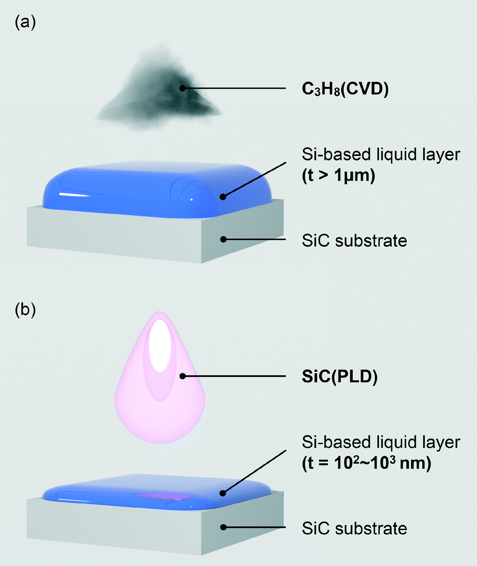 | ||
| Fig. 1 Comparison of (a) CVD-based and (b) PLD-based VLS processes of SiC thin film growth. | ||
In contrast, we have also proposed, independently from the group of Ferro et al., a similar VLS process in pulsed laser deposition (PLD) since 2002,11 and named the process “flux-mediated epitaxy (FME)” in 2005,12 to emphasize the roles of a flux in the vapor growth process. In this process, as shown in Fig. 1b, one distinct difference from the CVD-based VLS process by Ferro et al. is that a flux material is first deposited in a thin layer form of several tens to hundreds of nm in thickness, followed by continuous deposition of the growing film by PLD at a high temperature to melt the flux layer. Even through such a thin flux layer, we have succeeded in the fabrication of uniform single crystal oxide films such as superconducting NdBa2Cu3O7−x grown with a Ba–Cu–O self-flux11 and ferroelectric Bi4Ti3O12 with a Cu-stabilized BiOx flux available in vacuum.13 More recently, the FME concept has been extended to the growth of organic crystals/films of pentacene14 and fullerene (C60)15 with ionic liquids, which are a new class of organic solvents stable in liquid even in vacuum.
In the growth of SiC films, the advantages of the use of a flux layer as thin as possible include the ability to avoid the slow carbon diffusion limit to the total growth rate as well as its solubility limit being not a factor, i.e. the wide availability of the flux composition. It is because the material sources from the gas phase can reach the substrate to precipitate upon their dissolution into the liquid flux if the liquid flux layer is very thin even though the solubility is low. However, one possible problem is the thickness limitation. Unfortunately, Si-based fluxes generally will not spread homogeneously over the SiC surface, thus the uniform growth of SiC films seems not expected. In fact, the minimum thickness of a liquid flux layer is, at most, 2–3 μm for high-quality and uniform SiC thin films in the CVD-based VLS process.16
In this study, we demonstrate that a thin Si–Ni alloy layer can work effectively as a flux to produce a uniform SiC film. The key point is the simultaneous supply of pure Si and C sources from the gas phase by PLD using a SiC stoichiometric target, stabilizing the flux during the process. The high-temperature laser microscopy observation revealed that the Si–Ni alloy took a droplet form with several micrometers in diameter on SiC, apparently inconsistent with the uniform flux growth of SiC films. To explain this inconsistency, the possible existence of a “precursor film”, a nm-thick liquid film spreading between liquid droplets that can have a similar role in the flux process, will be discussed.
2. Experimental
2.1 Thin film fabrication
As a flux, a 1![[thin space (1/6-em)]](https://www.rsc.org/images/entities/char_2009.gif) :2 composition ratio of Ni to Si (NiSi2) was selected in this study on the basis of its lower melting point data, and better wettability on and more reactivity with SiC, as investigated in our previous laser microscopy study.17 First, a 150 nm-thick flux layer was deposited on 4H-SiC (0001) on-axis by PLD using a NiSi2 target with a KrF excimer laser (248 nm) at a repetition rate of 10 Hz and an energy density of 1.9 J cm−2 at room temperature. The sample was then mounted on a carbon plate (15 × 15 × 2t mm3) with carbon paste and heated from the backside of the carbon plate by a Nd:YAG laser; the sample temperature was measured using a radiation thermometer. After the sample temperature reached 1160 °C at which NiSi2 had melted, a 200 nm-thick SiC was deposited using a SiC target at a repetition rate of 2 Hz and an energy density of 3.8 J cm−2. During the deposition of NiSi2 and SiC, the backpressure was kept in high vacuum below 1 × 10⁻⁶ Torr. After the deposition, the remaining flux was removed from the film surface by etching with a HF:HNO3 (1:1) solution.
:2 composition ratio of Ni to Si (NiSi2) was selected in this study on the basis of its lower melting point data, and better wettability on and more reactivity with SiC, as investigated in our previous laser microscopy study.17 First, a 150 nm-thick flux layer was deposited on 4H-SiC (0001) on-axis by PLD using a NiSi2 target with a KrF excimer laser (248 nm) at a repetition rate of 10 Hz and an energy density of 1.9 J cm−2 at room temperature. The sample was then mounted on a carbon plate (15 × 15 × 2t mm3) with carbon paste and heated from the backside of the carbon plate by a Nd:YAG laser; the sample temperature was measured using a radiation thermometer. After the sample temperature reached 1160 °C at which NiSi2 had melted, a 200 nm-thick SiC was deposited using a SiC target at a repetition rate of 2 Hz and an energy density of 3.8 J cm−2. During the deposition of NiSi2 and SiC, the backpressure was kept in high vacuum below 1 × 10⁻⁶ Torr. After the deposition, the remaining flux was removed from the film surface by etching with a HF:HNO3 (1:1) solution.
2.2 Thin film and flux characterization
The surface morphology of the films and remaining flux after deposition was observed by scanning electron microscopy (SEM, S-4000, Hitachi High-Technologies Co., Ltd.) and atomic force microscopy (AFM, SPA-400, Seiko Instruments Inc.). Energy-dispersive X-ray spectrometry (EDX) with which the SEM was equipped was used to examine the composition of the flux. The polytypes of SiC in the film were identified, including their epitaxial relationships to the 4H-SiC (0001) substrate, by transmission electron microscopy (TEM) with electron diffraction (ED). The degree of excess carbon inclusion in the SiC film was also examined by TEM-EDX as well as Raman spectroscopy (RAMANOR T64000, Horiba, Ltd.).2.3 High-temperature laser microscopy observation in vacuum
During heating of a NiSi2-deposited 4H-SiC (0001) sample, the solid–liquid interface was directly observed by using a confocal laser microscope (LM, VK-X130/120, Keyence Corporation). In our system, the sample was heated by a Nd:YAG laser from the front side of the sample up to 1710 °C with a heating rate of 30 °C min−1 in high vacuum, while the laser probe was introduced from the backside of the substrate using an objective lens with a focal length of 20.5 mm.3. Results and discussion
3.1 Flux effects on the surface morphology, crystallinity and composition of SiC thin films
Fig. 2 shows a set of SEM images for samples just after depositing SiC without flux (a) and with flux (b). The former sample, grown without flux, shows granular structures all over the surface. The grain sizes are less than 1 μm, as is more clearly seen in the inset AFM image of Fig. 2a, which was taken over the surface after removing the remaining flux. In contrast, for the latter sample, grown with flux, the surface becomes very flat with some hemispherical droplets segregated on the surface. The composition analysis of these droplets by EPMA confirmed that they were the remaining flux. The droplet shape suggests that the NiSi2 flux film was once melted to form liquid droplets, inhomogeneously covering the growing SiC film surface during the deposition of SiC. Nevertheless, the obtained SiC film surface is more uniform for the flux droplet size of several micrometers, the mechanism of which will be discussed later in section 3.2. Furthermore, it exhibits a step-and-terrace structure with “triangle step” edges, as seen in the inset AFM image of Fig. 2b for the SiC surface after removing the remaining flux. The dominant “triangle edge” angle of 60 degrees, i.e. the three-fold symmetry of the surface step pattern, suggests that the polytype of the growing SiC film is 3C-SiC with the (111) face exposed.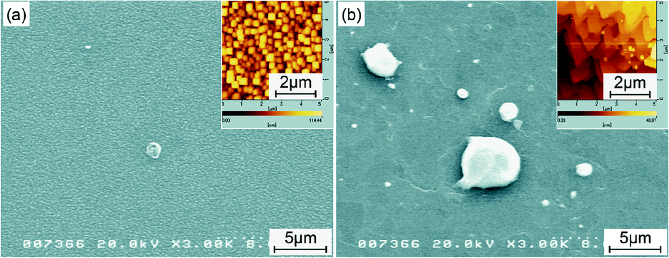 | ||
| Fig. 2 SEM images of SiC thin films grown (a) without and (b) with flux before removing the remaining flux. The insets are AFM images of the thin film surfaces after removing the remaining flux. | ||
Fig. 3a and b show a set of bright-field cross-sectional TEM images of SiC films grown without and with flux, respectively, after removing the remaining flux. The SiC thin film grown without flux shows granular structures not only on the surface, as is observed in the SEM, but also in the bulk including many voids therein. In contrast, the SiC thin film grown with Si–Ni flux was extremely uniform and almost no dislocations and grain boundaries can be found within an observable range. Fig. 3c and d show the expanded high-resolution TEM (HRTEM) images, together with their selected area diffraction patterns, of the SiC films shown in Fig. 3a and b, respectively. As is clearly identified in the HRTEM image and diffraction pattern in Fig. 3d, the SiC thin film grown with Si–Ni flux has a single phase of 3C-SiC, as is expected from the three-fold symmetry of the surface step pattern, growing along the <111> direction on 4H-SiC (0001). On the other hand, the diffraction pattern in Fig. 3c shows that the granular film consists of a mixture of 3C and 6H-SiC polytypes. In addition, often found near the interface are some pore-like features of 10 nm or less in diameter, as shown in the HRTEM image. The TEM-EDX analysis in Fig. 4a revealed that the pores were the result of carbon aggregation with a higher C/Si intensity ratio of 3.91, after calibrated so that the C/Si intensity in the SiC substrate is unity. In fact, the granular SiC film grown without flux has a carbon-rich composition with a C/Si intensity ratio of 1.24 on average, while the flux-grown SiC film has a C/Si intensity ratio of 1.01, almost a stoichiometric composition on average. These results are in good agreement with the macroscopic analysis by Raman spectroscopy as shown in Fig. 4b. Besides the peak around ∼1520 cm−1, an overtone of the TO (X) phonon modes of 4H-SiC18 and 3C-SiC,18,19 two carbon-associated broad peaks at 1350 cm−1 and ~1600 cm−1 are observed in the granular SiC film, but not in the 3C-SiC single crystal film. These peaks are assigned to the D-band20,21 and G-band, respectively. The G-band peak is typically located at 1580 cm−1 for bulk carbon, while it is likely to shift to around 1600 cm−1 for nano-graphite flakes.20,21 The G-band peak at ∼1600 cm−1 observed in the granular SiC film, therefore, should originate from nanometer-sized carbon clusters such as carbon nanopores found in the HRTEM image of the granular SiC thin film. The excess carbon inclusion in the SiC film grown without flux suggests that a non-negligible amount of Si in the total supplied from the SiC target by PLD is ready to evaporate again even at the optimal growth temperature of 1160 °C. Hence, the Si–Ni flux may have an additional role to compensate for the Si deficiency in the growth of SiC films at such a high growth temperature.
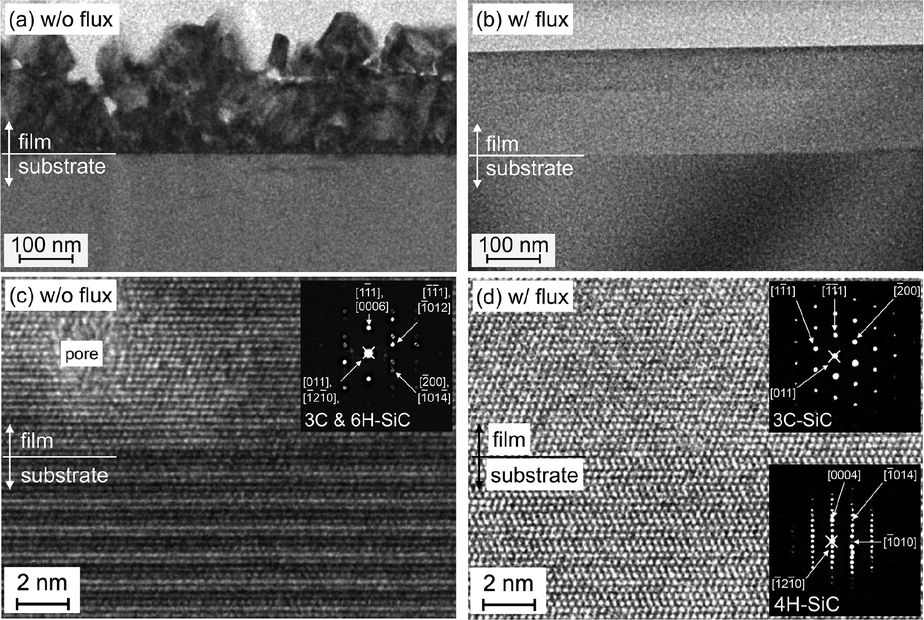 | ||
| Fig. 3 Bright-field cross-sectional TEM images of SiC films grown (a) without and (b) with flux after removing the remaining flux. (c and d) The expanded HRTEM images, together with their selected area diffraction patterns, of the corresponding SiC films in (a) and (b), respectively. | ||
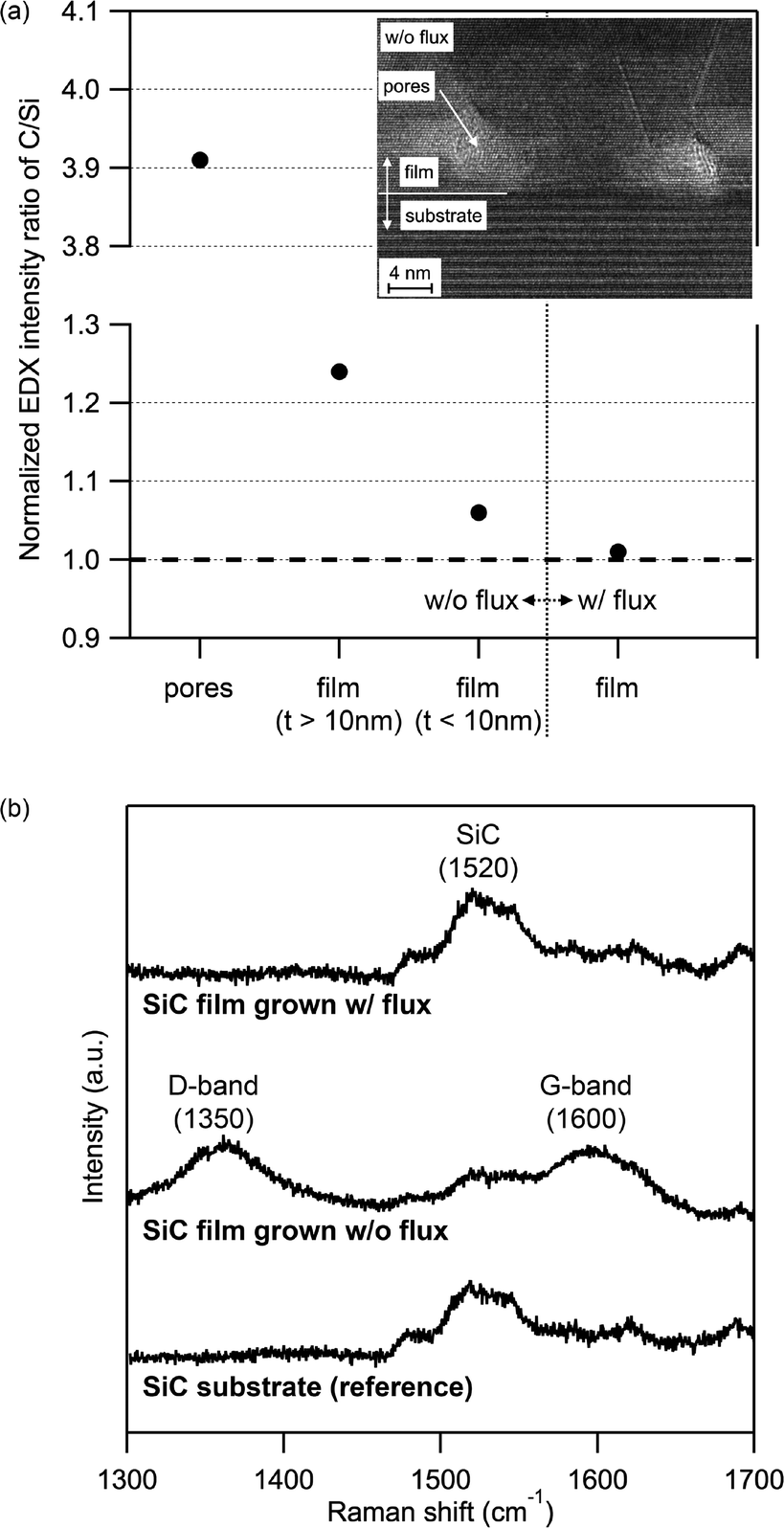 | ||
| Fig. 4 (a) Comparison of C/Si intensity ratios, analyzed by TEM-EDX, depending on the positions in the TEM image (inset). (b) Raman spectra of SiC films grown with and without flux, along with that of the 4H-SiC (0001) substrate as a reference. | ||
3.2 Mechanism of the uniform flux growth of SiC films via NiSi2 liquid droplets
As is already pointed out in section 3.1, we have succeeded in the uniform growth of SiC films with even a sub-micron thin alloy NiSi2 layer. However, the remaining flux droplets suggest that the NiSi2 flux was once melted to form liquid droplets inhomogeneously dispersed over the SiC surface during the deposition of SiC. In fact, according to our previous in situ laser microscopy study on the melting behavior of Ni–Si alloy films on a 4H-SiC substrate, many liquid droplets of NiSi2 are dispersed over the surface.17 Most of them will not move around, but will just stay near their original position around the growth temperature. Here, one question may arise: why is the flux effect so uniform over the sizes of flux droplets? One possible hypothesis is that there is a nm-thick liquid flux film spreading between liquid droplets that can have a similar role in the flux growth as shown in Fig. 5, as is pointed out also by Ferro and co-workers.22 The nm-thick film is historically well-known as a precursor film,23,24 for example in liquid-on-solid systems25,26 and metal-on-metal systems,27,28 although the precursor film is generally hard to detect because of its inherent nature of nm-thinness.25–30 The existence of such a precursor liquid flux film was also suggested by the step-bunching behaviour directly observed at the interface between the 4H-SiC (0001) on-axis substrate and NiSi2 flux thin film (150 nm) in the following LM experiment.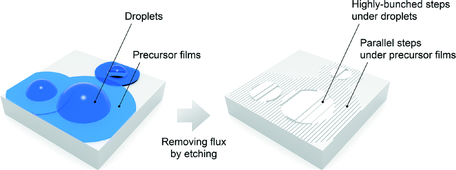 | ||
| Fig. 5 Schematic of possible precursor liquid flux film spreading around and between the flux droplets on the SiC surface. | ||
In the LM observation during the temperature increase, the NiSi2 flux thin film started to melt above 1100 °C, which is very close to the melting temperature of NiSi2, and completely became liquid droplets at 1160 °C, the details of which mechanism will be discussed elsewhere. We confirmed that once the droplets were formed, they were likely to stay almost at their original position even after further temperature increase, as is pointed out above. Fig. 6a–c show sequential LM images just focused on the interface of the substrate with the temperature maintained at 1710 °C. The circular regions imaged in white, indicating a higher reflection intensity of the incident probe laser on the gray scale, are those underneath the droplets, and thus the circular shape is just a silhouette of the droplet. In contrast, the regions around and between the droplets are imaged in gray, indicating a lower reflection intensity due to the transparent nature of SiC to the probe laser light.
 | ||
| Fig. 6 (a–c) Laser microscopy images of the interface between the SiC substrate and flux at 1710 °C. The step-bunching behavior of the SiC substrate in contact with the flux was clearly observed. (d) AFM image of the surface after removing the flux for the sample observed in (a–c). (e–h) Laser microscopy and AFM images of the SiC substrate without flux observed under the same conditions as those in (a–d) as reference. | ||
In Fig. 6c, we can clearly see that some meandering steps, imaged as dark lines, gradually appear underneath the droplets, indicative of the formation of step-bunched structures, and such a distinct morphological change was observed after reaching the temperature mentioned above. On the other hand, the parallel steps also can be found to run around and between the droplets, whose step-heights were estimated to be 20 to 30 nm by AFM as shown in Fig. 6d after removing the flux. In contrast, as shown in Fig. 6e–g, no formation of step-bunching structures is observed for a bare SiC surface as a reference, in which other experimental conditions were exactly the same as those when heating with the flux. In order to rule out a possible detection limit by the LM, the etched sample surface was also observed by AFM, as shown in Fig. 6h, to confirm that no step-bunching structures are formed. It is therefore concluded that the step-bunching definitely resulted from the etching by the liquid flux. The observation that the step-bunching also occurred even around and between the NiSi2 droplets on SiC also strongly suggests the precursor liquid flux film of NiSi2 covering almost the entire surface of SiC, as illustrated in Fig. 5. The thickness should be very thin, on the nm scale, because of almost no reflection intensity of the probe laser light in areas around and between the droplets. A similar situation is expected in the growth process by PLD and the possible precursor film may have an important role in the uniform growth of SiC films even though such a sub-micron alloy NiSi2 layer (∼150 nm) was used as the flux.
Here, it should be pointed out that the possibility of a bunch of very small mobile flux droplets even invisible through LM between micro-droplets, having a similar flux effect, cannot be completely ruled out at the moment. However, if there were such very small mobile droplets between micro-Ni silicide droplets, the growth of SiC nanowires or islands rather than uniform SiC films in our PLD process, though it may depend on the laser fluence, would be dominant as well.31–33
4. Conclusions
We successfully grew a high-quality 3C-SiC single crystal film by the PLD-based VLS process with a thin NiSi2 layer flux, even as small as 150 nm in thickness to form liquid droplets. The existence of a precursor liquid flux film spreading around and between the droplets was proposed to explain the uniformity of the obtained SiC film. Such a possible precursor film could also explain the step-bunching behaviour even around and between the NiSi2 droplets on SiC, as was directly visualized by high-temperature LM in vacuum. Although there has not yet been any direct evidence for such a precursor film, it would be a useful hypothesis for further development of the PLD-based VLS process for fabricating high-quality SiC films with a higher growth rate.Acknowledgements
This study was conducted under the Advanced Low Carbon Technology Research and Development Program (ALCA).Notes and references
- R. Tanaka, K. Seki, S. Komiyama, T. Ujihara and Y. Takeda, Mater. Sci. Forum, 2009, 600–603, 59 CrossRef CAS.
- Y. Yonezawa, M. Ryo, A. Takigawa and Y. Matsumoto, Sci. Technol. Adv. Mater., 2011, 12, 054209 CrossRef.
- K. Danno, H. Saitoh, A. Seki, H. Daikoku, Y. Fujiwara, I. Ishii, H. Sakamoto and Y. Kawai, Mater. Sci. Forum, 2010, 645–648, 13 CrossRef CAS.
- T. Mitani, N. Komatsu, T. Takahashi, T. Kato, K. Fujii, T. Ujihara, Y. Matsumoto, K. Kurashige and H. Okumura, J. Cryst. Growth, 2014, 401, 681 CrossRef CAS.
- O. Filip, B. Epelbaum, M. Bickermann and A. Winnacker, J. Cryst. Growth, 2004, 271, 142 CrossRef CAS.
- M. Soueidan and G. Ferro, Adv. Funct. Mater., 2006, 16, 975 CrossRef CAS.
- K. Kusunoki, S. Munetoh, K. Kamei, M. Hasebe, T. Ujihara and K. Nakajima, Mater. Sci. Forum, 2004, 457–460, 123 CrossRef CAS.
- T. Yoshikawa, S. Kawanishi and T. Tanaka, Jpn. J. Appl. Phys., 2010, 49, 051302 CrossRef.
- G. Ferro, D. Chaussende, F. Cauwet and Y. Monteil, Mater. Sci. Forum, 2002, 389–393, 287 CrossRef CAS.
- G. Ferro and C. Jacquier, New J. Chem., 2004, 28, 889 RSC.
- K. S. Yun, B. D. Choi, Y. Matsumoto, J. H. Song, N. Kanda, T. Itoh, M. Kawasaki, T. Chikyow, P. Ahmet and H. Koinuma, Appl. Phys. Lett., 2002, 80, 61 CrossRef CAS.
- Y. Matsumoto, R. Takahashi and H. Koinuma, J. Cryst. Growth, 2005, 275, 325 CrossRef CAS.
- R. Takahashi, Y. Yonezawa, M. Ohtani, M. Kawasaki, K. Nakajima, T. Chikyow, H. Koinuma and Y. Matsumoto, Adv. Funct. Mater., 2006, 16, 485 CrossRef CAS.
- Y. Takeyama, S. Maruyama and Y. Matsumoto, Cryst. Growth Des., 2011, 11, 2273 CAS.
- Y. Takeyama, S. Maruyama, H. Taniguchi, M. Itoh, K. Ueno and Y. Matsumoto, CrystEngComm, 2012, 14, 4939 RSC.
- A. Vo-Ha, D. Carole, M. Lazar, D. Tournier, F. Cauwet, V. Soulière, N. Thierry-Jebali, P. Brosselard, D. Planson, C. Brylinski and G. Ferro, Thin Solid Films, 2013, 548, 125 CrossRef CAS.
- S. Maruyama, A. Onuma, K. Kurashige, T. Kato, H. Okumura and Y. Matsumoto, ACS Comb. Sci., 2013, 15, 287 CrossRef CAS PubMed.
- W. J. Choyke, D. R. Hamilton and L. Patrick, Phys. Rev., 1964, 133, A1163 CrossRef.
- D. Olego and M. Cardona, Phys. Rev. B: Condens. Matter Mater. Phys., 1982, 25, 1151 CrossRef CAS.
- D. S. Knight and W. B. White, J. Mater. Res., 1989, 4, 385 CrossRef CAS.
- A. C. Ferrari and J. Robertson, Phys. Rev. B: Condens. Matter Mater. Phys., 2000, 61, 14095 CrossRef CAS.
- D. Chaussende, G. Ferro and Y. Monteil, J. Cryst. Growth, 2002, 234, 63 CrossRef CAS.
- W. B. Hardy, Philos. Mag., 1919, 38, 49 CrossRef CAS.
- M. N. Popescu, G. Oshanin, S. Dietrich and A.-M. Cazabat, J. Phys.: Condens. Matter, 2012, 24, 243102 CrossRef CAS PubMed.
- D. Beaglehole, J. Phys. Chem., 1989, 93, 893 CrossRef CAS.
- B. Drevillon, J. Perrin, R. Marbot, A. Violet and J. L. Dalby, Rev. Sci. Instrum., 1982, 53, 969 CrossRef CAS.
- J. Moon, J. Lowekamp, P. Wynblatt, S. Garoff and R. M. Suter, Surf. Sci., 2001, 488, 73 CrossRef CAS.
- J. Moon, P. Wynblatt, S. Garoff and R. Suter, Surf. Sci., 2004, 559, 149 CrossRef CAS.
- F. Heslot, A.-M. Cazabat and N. Fraysse, J. Phys.: Condens. Matter, 1989, 1, 5793 CrossRef.
- A.-M. Cazabat, Adv. Colloid Interface Sci., 1991, 34, 73 CrossRef CAS.
- S. K. Panda, J. Sengupta and C. Jacob, J. Nanosci. Nanotechnol., 2010, 10, 3046 CrossRef CAS PubMed.
- Z. Li, M. Zhang and A. Meng, CrystEngComm, 2011, 13, 4097 RSC.
- A. Marcu, T. Yanagida, K. Nagashima, H. Tanaka and T. Kawai, J. Appl. Phys., 2007, 102, 016102 CrossRef.
| This journal is © The Royal Society of Chemistry 2016 |