
Effects of side groups on the kinetics of charge carrier recombination in dye molecule-doped multilayer organic light-emitting diodes†
Shengwei
Shi
*ab,
Feng
Gao
b,
Zhengyi
Sun
b,
Yiqiang
Zhan
c,
Mats
Fahlman
b and
Dongge
Ma
a
aState Key Laboratory of Polymer Chemistry and Physics, Changchun Institute of Applied Chemistry, Chinese Academy of Sciences, Changchun, 130022, China
bDepartment of Physics, Chemistry and Biology, Linköping University, SE-58183 Linköping, Sweden. E-mail: shesh@ifm.liu.se
cState Key Laboratory of ASIC and System, Department of Microelectronics, SIST, Fudan University, Shanghai, 200433, China
First published on 10th November 2014
Abstract
The carrier recombination coefficient (γ) in dye molecule-doped multilayer organic light-emitting diodes was quantified by transient electroluminescence. It was found that γ and device efficiency were both strongly dependent on the molecular structures of the dopants.
Organic light-emitting diodes (OLEDs) have been extensively studied for their promising applications in flexible displays1 and solid state lighting.2,3 High performance organic materials, new device structures and advanced processing technologies are developed to advance the development of the OLED community.4–6 So far, OLEDs have been the most successful application of organic semiconductors. It is well acknowledged that electrical processes in OLEDs include three key steps, i.e. charge injection, charge transport, and charge carrier recombination. All of these three processes play very important roles in device performance.7–11
Transient electroluminescence (EL) (time resolved EL) has been widely used to investigate the electrical processes in OLEDs, enabling us to analyse charge transport and recombination in OLEDs.12–22 When a square voltage pulse is applied over the device, the EL starts to rise with a time delay, which has been interpreted as the transit time of the majority charge carriers. As the RC time constant of the setup is well below the delay time, it is unlikely that the RC constant is responsible for the delay time. The interpretation of the response time of the device in terms of transit time gives the mobility value.12–18 When the square voltage pulse is removed, the EL starts to decay, and it gradually decreases to zero EL. This decay time is closely related to bimolecular recombination of electrons and holes. The recombination coefficient (γ) then can be obtained from the decay part in transient EL,19–21 which is considered to be very important to understand the operating mechanism in OLEDs. However, most mechanistic investigations of OLEDs from transient EL are focused on the simple structure of electron-transport layer/emissive layer/hole-transport layer;12–21 there are very less device physics studies on the multilayer structure,22 which is adopted in practical applications. In addition, although many highly efficient molecules are developed in OLEDs, with different side groups to adjust the solubility,23 suppress the crystallization at the ITO/organic interface,24 reduce concentration quenching in phosphorescence,25 or inhibit the aggregation light-emission,26 it is still not clear how these side groups affect the device efficiency from the understanding of device physics.
In this communication, we employed transient EL to investigate charge carrier recombination in multilayer OLEDs. We used dye-doped CBP to work as the emissive layer. By keeping the backbone the same and changing the side groups, we were able to quantify the effect of the side groups on charge carrier recombination, and hence the device performance. The recombination coefficient (γ) of charge carriers is obtained from the decay part of transient EL through elaborate design of the device structure. Our results are in good agreement with the predictions of the Langevin model of charge carrier recombination assuming that the process is controlled by charge carrier diffusion.27 The analysis of charge carrier recombination kinetics clearly demonstrates that the donor groups and π-conjugated structure of the molecule ensure high EL efficiency with the same EL spectra. Based on the results of device performance and transient EL, we discuss the relationship between γ and molecular structure, which may guide the molecule design by modification of side groups to realize highly efficient OLEDs.
The device had a molecule-doped multilayer structure with pre-cleaned indium-tin-oxide (ITO) as the anode and aluminium (Al) as the cathode. N,N′-Bis(naphthalen-1-yl)-N,N′-bis(phenyl)benzidine (NPB) and tris(8-hydroxyquinoline)aluminium (Alq3) were used as hole and electron transport layers, respectively. 4,4′-Bis(N-carbazolyl)-1,1′-biphenyl (CBP) was employed as the host, and bathocuproine (BCP) worked as the hole blocking layer. LiF was deposited as the buffer layer. Dye molecules with different side groups were used as dopants (Fig. 1).
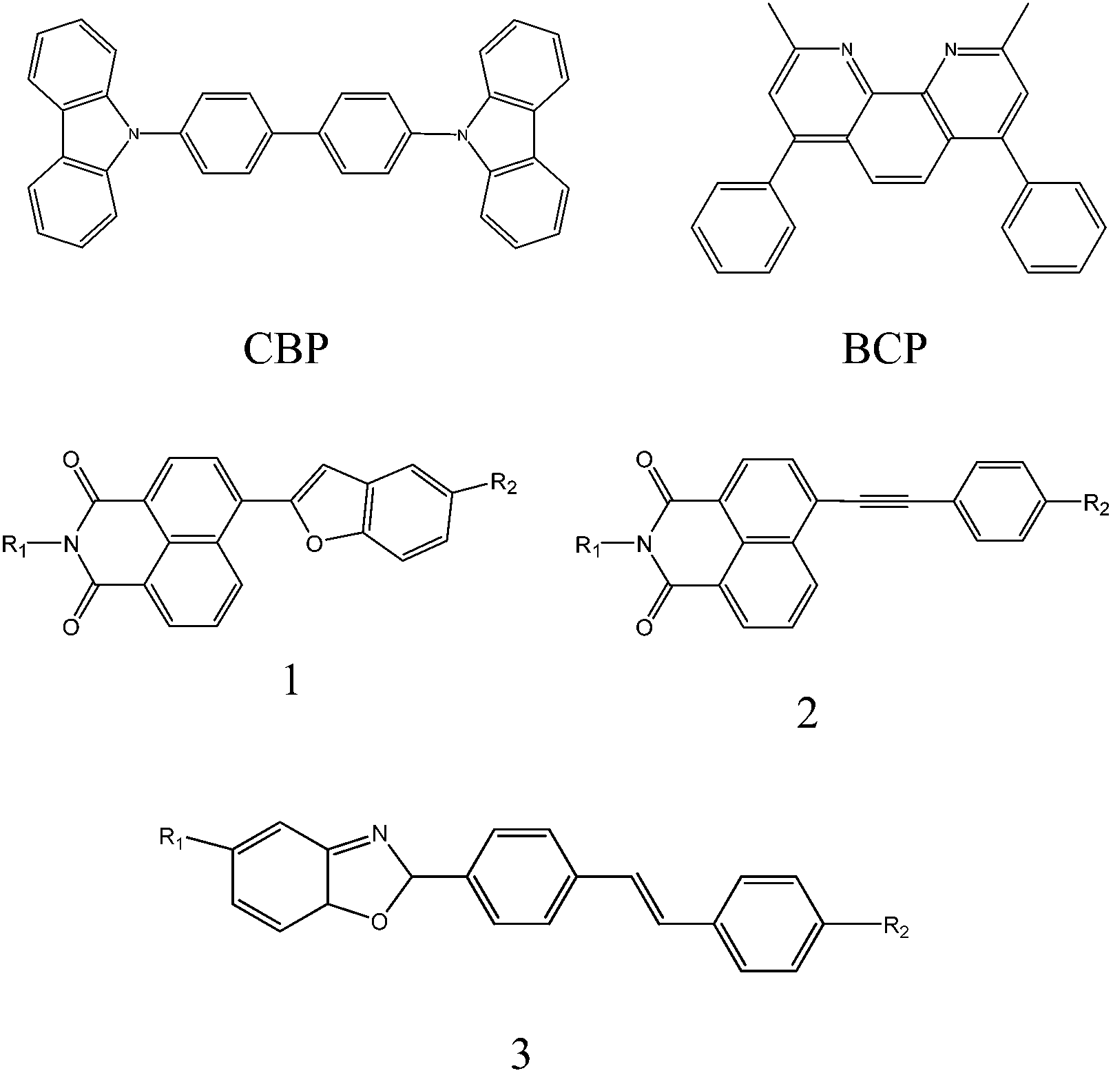 | ||
| Fig. 1 Chemical structures of CBP, BCP, molecule 1: N-alkyl-4-benzofuran-1,8-naphthalimides, molecule 2: N-alkyl-4-arylacetylene-1,8-napthalimides and molecule 3: 2-(E)-stilbene benzoxazole (R1 and R2 indicate side groups in the molecules). | ||
The devices were fabricated with the structure: ITO/NPB (40 nm)/CBP:X (1%) (20 nm)/BCP (20 nm)/Alq3 (40 nm)/LiF (1 nm)/Al (200 nm), in which X indicates the dye molecules used in the experiments (Fig. 2). All layers were prepared in a high-vacuum chamber with the pressure less than 5 × 10⁻⁴ Pa by thermal evaporation without breaking the vacuum. All organic films except dye molecules were deposited at a rate of 0.1–0.3 nm s−1, and the doping (1%) was realized by controlling the rate ratio between the host and dye molecules. LiF and Al were deposited at a rate of 0.01 nm s−1 and 0.8–1.0 nm s−1, respectively. The rate is determined by a calibrated quartz microbalance, and the active area is 3 × 3 mm2.
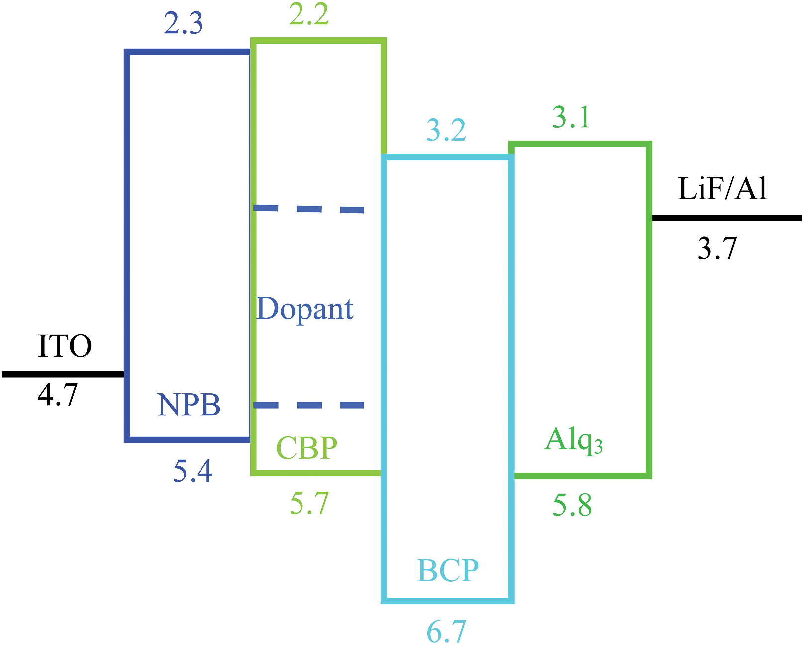 | ||
| Fig. 2 Device structure and energy levels for dye molecule doped multilayer OLEDs. | ||
Current density–luminance–voltage (J–L–V) characteristics were measured using a Keithley source meter unit (Keithley 2400 and Keithley 2000) with a calibrated silicon photodiode. The EL spectra were measured using a JY SPEX CCD3000 spectrometer. The UV-vis and PL spectra were measured using a PerkinElmer Lambda 35 UV-vis spectrometer and a PerkinElmer LS 50B spectrofluorometer, respectively. For the transient EL, an Agilent 8114A 100 V/2A programmable pulse generator was used to apply a rectangular voltage pulse to the devices. The repetition rate of the pulse was 1 kHz, and the pulse length was 20 μs. The time-dependent EL signals were detected by the 50 Ω input resistance of a digital oscilloscope (Agilent Model 54825A, 500 MHz/2 Gs/s) together with a photomultiplier (time resolution ≅ 0.65 ns) located directly on top of the emitting devices. All measurements were carried out at room temperature under ambient conditions.
The dye molecule dopants used in this experiment are derivatives of naphthalimide and stilbene, which have been reported to be very promising molecules in OLEDs. They have very good photochemical and thermal stability, and their molecular structures can be easily modified to obtain colour adjustable emission.28–33 We use three different dye molecules (Fig. 1) in the experiments. Considering that consistent results can be drawn from these three different molecules, we focus on the discussions on molecule 1 in the main text and leave molecules 2 and 3 in the ESI.†Table 1 summarises the physical properties of molecule 1 with different side groups.
| Sample | R1 | R2 | λ UV,max (nm) | λ FL,max (nm) | Melt point (°C) |
|---|---|---|---|---|---|
| 1a | n-Bu | t-Bu | 397.0 | 508.5 | 170.0–171.5 |
| 1b | n-Bu | CH3 | 398.5 | 508.0 | 140.0–141.0 |
| 1c | n-Bu | Cl | 386.5 | 493.0 | 174.5–176.0 |
| 1d | n-Hexyl | CN | 378.5 | 470.0 | 213.0–214.0 |
The device structure is shown in Fig. 2 and the related energy levels are collected from the ref. 34–36. As shown in Fig. 3a, four devices have almost the same EL spectra peaked at around 500 nm. This peak is significantly different from the peak at ∼550 nm from pure Alq3,37 meaning that the carrier recombination is mainly confined in the molecule doping layer. At the same time, we notice that the four molecules with different side groups give very different device performance (Fig. 3b). Table 2 lists the performance of all four devices. Device 1a has the highest current efficiency of 3.7 cd A−1 with a luminance of 3640 cd m−2, while device 1d gives the lowest efficiency (less than 1 cd A−1) with a luminance of about 760 cd m−2. The performance of devices 1b and 1c lies between that of 1a and 1d.
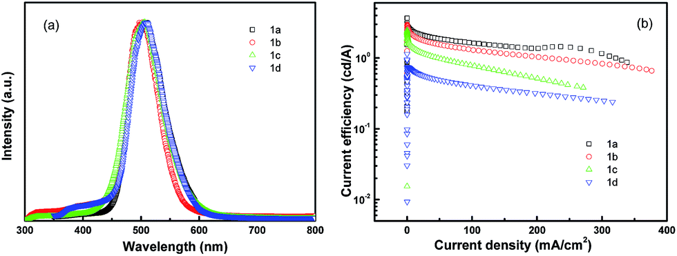 | ||
| Fig. 3 Device performance of dye molecule-doped multilayer OLEDs with molecule 1 doping. (a) EL spectra and (b) current efficiency–current density. | ||
| Slope (S) | Intercept (A) | γ (10−12 cm3 s−1) | Efficiency (cd A−1) | Luminance (cd m−2) | |
|---|---|---|---|---|---|
| a The unit is 106 (cm3 s−1)1/2 for S, and (cm3 s)1/2 for A. | |||||
| 1a | 2.25 | 2.22 | 5.80 ± 0.05 | 3.7 | 3640 |
| 1b | 2.03 | 2.11 | 5.22 ± 0.05 | 3.0 | 2550 |
| 1c | 3.32 | 4.09 | 3.72 ± 0.05 | 2.5 | 1040 |
| 1d | 1.28 | 2.48 | 1.50 ± 0.05 | 0.8 | 760 |
In order to understand the operation mechanisms of the devices as well as the physics behind the significant difference between these four devices, we examined their J–V curves. As shown in Fig. 4a, all the J–V characteristics follow power-law dependence, which has been proposed to be charge-trap limited transport.38,39 Assuming an exponential trap energy distribution, the J–V relationship can be described by J ∼ Vm+1, where m = Tt/T with T being the absolute temperature and Tt being the characteristic temperature of the trap distribution. The value of the exponent m is related to trap concentrations and mobility, and a higher value of m means deeper traps in the devices. All the four devices share an exponent value of around 9, indicating that there are similar trap distributions in the four devices. Considering that the dye dopants have similar molecular structures, it is reasonable that the four devices have similar trap distributions. The fact that the current is dominated by traps also indicates that J–V curves are determined by the bulk properties rather than by contact effects.19
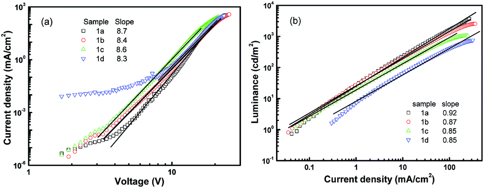 | ||
| Fig. 4 Steady state characterization of the devices with molecule 1 doping. (a) Current density–voltage and (b) luminance–current density. | ||
Further information regarding the device operation is revealed by the luminance–current density (L–J) curves. As shown in Fig. 4b, all the L–J curves have a linear relationship in the log–log plot with a slope of 1 at high electric fields, meaning that the devices work in the volume-controlled EL mode,19 consistent with our conclusion based on the J–V curves. Both the power-law dependence of J–V and the linear relation of L–J confirm the Langevin bimolecular recombination in the devices.27 Holes injected from the ITO are transported through the hole transport layer NPB to the doping emission layer, and their transport to the Alq3 side is blocked by the BCP layer because of a high injection barrier at the CBP/BCP interface. Therefore, holes are confined in the doped emission layer and have to wait for the electrons to arrive. Electrons injected from the LiF/Al cathode are transported through the electron transport layer Alq3 and the hole blocking layer BCP. Electrons finally transport to the doped emission layer to recombine with the waiting holes, producing light emission from the dye molecule. The low mobility of NPB and Alq3 makes the effective transit time in the device very long, resulting in high recombination probability.12,19 As a result, the devices operate in the volume-limited mode.
For volume-limited current, with bimolecular recombination in the narrow zone of the emission layer being the main channel for carrier decay, the free carrier kinetics can be described by the following equations:19
 | (1) |
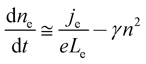 | (2) |
Although the hole mobility in NPB is larger than the electron mobility in Alq3, there is a high barrier at the CBP/BCP interface for hole injection into the Alq3 layer. As a result, the excess holes will accumulate in the doped emission layer near the CBP/BCP interface. For electrons, it is easier for them to inject through BCP to the emission layer. Therefore the light-emission is dominated by the recombination in the doped layer rather than in Alq3, as confirmed by the spectra results. In addition, because of the relatively large value of the columbic capture radius, the recombination time is substantially shorter than the trapping time. This means that the injected electrons and holes in the recombination zone will recombine rapidly, and hence no excess charge carriers exist. Consequently, except for the accumulated holes, holes as well as electrons in the recombination zone may be considered to be free and approximately equal to each other in concentration (nh ≅ ne = n). The charge decay, after the voltage pulse is turned off, can then be simplified as
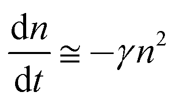 | (3) |
Thus,
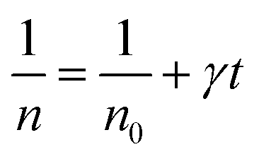 | (4) |
Taking into account the EL yield,
| ΦEL = φPLPsγ[n(t)]2 | (5) |
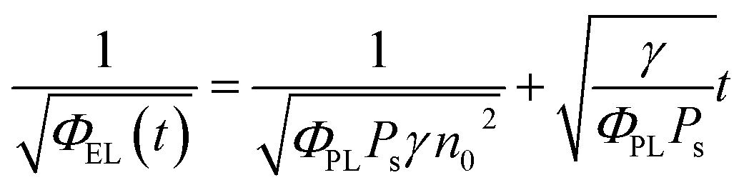 | (6) |
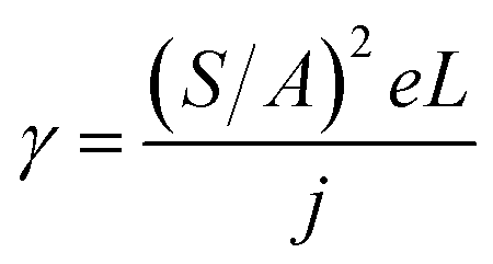
This equation clearly indicates that the reciprocal of the square root of the decay EL intensity is in linear relationship with the time scale. From the ratio of slope S = (γ/φPLPs)1/2 to intercept A = (φPLPsγn02)−1/2, the electron–hole recombination coefficient can then be calculated as:
 | (7) |
Eqn (7) enables us to investigate the charge carrier recombination immediately after switching off the bias. Therefore, here we employed transient EL to investigate charge carrier recombination in the devices, aiming to further understand the difference between these four devices.
Fig. 5a shows the transient EL intensity–time relationship in dye molecule-doped OLEDs at the same equilibrium current of 170 mA cm−2, and it shows different EL decay curves for devices with different doping molecules, providing useful information on charge carrier recombination in different devices. In order to quantify the charge carrier recombination, we further plot the transient EL decay (φEL)−1/2versus time in Fig. 5b, where the inset shows the φEL(t) decay curves. Here t = 0 corresponds to the voltage fall of the pulse. Perfect straight lines can be fitted to the experimental data within the experimental error range. The values of slopes (S) and intercepts (A) are obtained from the linear relationship, and then the charge carrier recombination coefficient γ can be calculated with j = 170 mA cm−2 and L = 60 nm (refer to eqn (7)). The values are summarised in Table 2. The device with molecule 1a doping has shown the highest γ of (5.80 ± 0.05) × 10−12 cm3 s−1, which is nearly four times higher than that of the lowest value of (1.50 ± 0.05) × 10−12 cm3 s−1 for the device with molecule 1d doping. As is well known, high γ means that highly efficient recombination of holes and electrons in the devices. Therefore the fitted γ values are consistent with the device performance, with the device with molecule 1a showing the highest efficiency. Considering that the only difference between different molecules lies in the side groups, it is reasonable to conclude that the difference in EL efficiency may result from the side groups. As reported before, the donor group (e.g. in molecule 1a) is considered to form a strong push–pull electron structure, and hence the electron can easily transfer to the aromatic ring to form an expanded π-conjugated structure, enhancing fluorescence emission from the molecule backbone,28,29 while the strong acceptor group (e.g. in molecule 1d) will decrease the fluorescence emission as it reduces the electron density in the system. Indeed, in our experiments, donor groups ensure higher EL efficiency for the molecule-doping multilayer OLEDs, and the higher γ values are consistent with the device results.
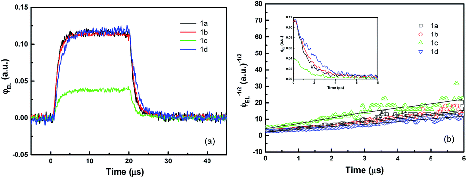 | ||
| Fig. 5 Transient EL characterization of the devices with molecule 1 doping. (a) Transient EL intensity–time and (b) comparison of the transient EL decay at the same equilibrium current density of 170 mA cm−2 plotted in (φEL)−1/2versus time scale. The φEL(t) decay curves are shown in the inset. Here t = 0 corresponds to the voltage fall of the pulse. | ||
We have also extended our measurements to other molecules to generalise our observations. For molecule 2, we obtain similar results and conclusions to molecule 1 (see ESI Fig. s1 and s2†), in which the donor groups, such as –CH3, guarantee higher γ and EL efficiency, while the acceptor groups, such as –F and –CF3, decrease the γ and EL efficiency. Molecule 3, though a little bit complicated, also shows results consistent with molecules 1 and 2. The R1 group shows stronger donor characteristics in 3a and 3b (t-Bu) than in 3c (–H). In addition, the R2 group, –COOCH3 (3a) and p-C6H6 (3b), can bring a bigger π-conjugated structure than 2,5-OCH3 (3c) in the backbone. Therefore, more delocalized electrons can be excited, and thus the devices with molecules 3a and 3b show higher γ and EL efficiency compared with molecule 3c (Fig. s3 and s4†).
In conclusion, multilayer OLEDs were designed and fabricated based on molecule-doping technology, in which the derivatives of naphthalimide and stilbene with different side groups were used as the dopants in the CBP host as the light-emission layer. All devices for each set of molecules showed almost the same EL spectra, but very different efficiency. Transient EL, by which the kinetics of the charge carrier recombination was investigated, was used to understand the physics behind the different EL efficiency. The coefficient (γ) of electron–hole recombination was determined from the long-time component of the temporal decay of the EL intensity after a rectangular voltage pulse was turned off. It was found that γ and EL efficiency were both strongly dependent on the side groups of the dopants. Donor structures in the side groups guarantee much higher γ and EL efficiency than the acceptor ones. Our results provide a promising guide for the structural design of molecular materials in highly efficient OLEDs. Chemists can slightly change the side groups to maintain the desired emission spectra while significantly enhancing the device efficiency. In addition, this report may provide useful hints on how to design molecule structures to reduce charge carrier recombination, which is considered to be the main cause of efficiency loss in organic solar cells.40–42
Acknowledgements
We thank Prof. Longhe Xu from the Dalian University of Technology for providing the molecules. Dr Ma thanks the financial support of the Hundreds Talents Program, Chinese Academy of Sciences and the National Science Fund for Distinguished Young Scholars of China (50325312). F.G. acknowledges the financial support of the European Commission under a Marie Curie Intra-European Fellowship for Career Development.Notes and references
- G. Gustafsson, Y. Cao, G. M. Treacy, F. Klavetter, N. Colaneri and A. J. Heeger, Nature, 1992, 357, 477–479 CrossRef CAS.
- B. W. D'Andrade and S. R. Forrest, Adv. Mater., 2004, 16, 1585–1595 CrossRef.
- S. Reineke, F. Lindner, G. Schwartz, N. Seidler, K. Walzer, B. Lussem and K. Leo, Nature, 2009, 459, 234–238 CrossRef CAS PubMed.
- L. Xiao, Z. Chen, B. Qu, J. Luo, S. Kong, Q. Gong and J. Kido, Adv. Mater., 2011, 23, 926–952 CrossRef CAS PubMed.
- M. C. Gather, A. Köhnen and K. Meerholz, Adv. Mater., 2011, 23, 233–248 CrossRef CAS PubMed.
- G. Schwartz, S. Reineke, T. C. Rosenow, K. Walzer and K. Leo, Adv. Funct. Mater., 2009, 19, 1319–1333 CrossRef CAS.
- W. Brutting, S. Berleb and A. G. Muckl, Org. Electron., 2001, 2, 1–36 CrossRef CAS.
- M. A. Baldo and S. R. Forrest, Phys. Rev. B: Condens. Matter Mater. Phys., 2001, 64, 085201 CrossRef.
- J. C. Scott, J. Vac. Sci. Technol., A, 2003, 21, 521–531 CAS.
- G. G. Malliaras and J. C. Scott, J. Appl. Phys., 1998, 83, 5399–5403 CrossRef CAS PubMed.
- Y. Shirota and H. Kageyama, Chem. Rev., 2007, 107, 953–1010 CrossRef CAS PubMed.
- T. C. Wong, J. Kovac, C. S. Lee, L. S. Hung and S. T. Lee, Chem. Phys. Lett., 2001, 334, 61–64 CrossRef CAS.
- S. Barth, P. Muller, H. Reil, P. F. Seidler, W. Rieß, H. Vestweber and H. Bassler, J. Appl. Phys., 2001, 89, 3711–3719 CrossRef CAS PubMed.
- H. Chayet, R. Pogreb and D. Davidov, Phys. Rev. B: Condens. Matter Mater. Phys., 1997, 56, R12702 CrossRef CAS.
- P. W. M. Blom and M. C. J. M. Vissenberg, Phys. Rev. Lett., 1998, 80, 3819–3822 CrossRef CAS.
- D. J. Pinner, R. H. Friend and N. Tessler, J. Appl. Phys., 1999, 86, 5116–5130 CrossRef CAS PubMed.
- Y. H. Tak, J. Pommerehme, H. Vestweber, R. Sander, H. Bassler and H. H. Horhold, Appl. Phys. Lett., 1996, 69, 1291–1293 CrossRef CAS PubMed.
- J. Chen and D. Ma, J. Appl. Phys., 2004, 95, 5778–5781 CrossRef CAS PubMed.
- J. Kalinowski, N. Camaioni, P. Di Marco, V. Tattori and A. Martelli, Appl. Phys. Lett., 1998, 72, 513–515 CrossRef CAS PubMed.
- J. Chen and D. Ma, J. Phys. D: Appl. Phys., 2006, 39, 2044–2047 CrossRef CAS.
- J. Chen, D. Ma, Y. Liu and Y. Wang, J. Phys. D: Appl. Phys., 2005, 38, 3366–3370 CrossRef CAS.
- M. A. Baldo and S. R. Forrest, Phys. Rev. B: Condens. Matter Mater. Phys., 2000, 62, 10958–10966 CrossRef CAS.
- J. H. Park, C. Yun, M. H. Park, Y. Do, S. Yoo and M. H. Lee, Macromolecules, 2009, 42, 6840–6843 CrossRef CAS.
- S. E. Shaheen, G. E. Jabbour, B. Kippelen, N. Peyghambarian, J. D. Anderson, S. R. Marder, N. R. Armstrong, E. Bellmann and R. H. Grubbs, Appl. Phys. Lett., 1999, 74, 3212–3214 CrossRef CAS PubMed.
- C. Rothe, C. J. Chiang, V. Jankus, K. Abdullah, X. Zeng, R. Jitchati, A. S. Batsanov, M. R. Bryce and A. P. Monkman, Adv. Funct. Mater., 2009, 19, 2038–2044 CrossRef CAS.
- S. Setayesh, A. C. Grimsdale, T. Weil, V. Enkelmann, K. Mullen, F. Meghdadi, E. J. W. List and G. Leising, J. Am. Chem. Soc., 2001, 123, 946–953 CrossRef CAS PubMed.
- M. Pope and C. E. Swenberg, Electronic Processes in Organic Crystals, Oxford University Press, Oxford, 1982 Search PubMed.
- J. X. Yang, X. L. Wang, X. M. Wang and L. H. Xu, Dyes Pigm., 2005, 66, 83–87 CrossRef CAS PubMed.
- J. X. Yang, X. L. Wang, S. Tong and L. H. Xu, Dyes Pigm., 2005, 67, 27–33 CrossRef CAS PubMed.
- P. Wang, Z. Xie, S. Tong, O. Wong, C. S. Lee, N. Wong, L. Hung and S. T. Lee, Chem. Mater., 2003, 15, 1913–1917 CrossRef CAS.
- W. Zhu, L. Fan, R. Yao, F. Wu and H. Tian, Synth. Met., 2003, 137, 1129–1130 CrossRef CAS.
- A. Kukhta, E. Kolesnik, M. Taoubi, D. Drozdova and N. Prokopchuk, Synth. Met., 2001, 119, 129–130 CrossRef CAS.
- I. Fuks-Janczarek, I. V. Kityk, R. Miedzinski, E. Gondek, J. Ebothe, L. Nzoghe-Mendome and A. Danel, J. Mater. Sci.: Mater. Electron., 2007, 18, 519–526 CrossRef CAS.
- S. Shi and D. Ma, Semicond. Sci. Technol., 2005, 20, 1213–1216 CrossRef CAS.
- M. A. Baldo, S. Lamansky, P. E. Burrows, M. E. Thompson and S. R. Forrest, Appl. Phys. Lett., 1999, 75, 4–6 CrossRef CAS PubMed.
- T. Zhang, Y. Liang, J. Cheng and J. Li, J. Mater. Chem. C, 2013, 1, 757–764 RSC.
- C. W. Tang and S. A. VanSlyke, Appl. Phys. Lett., 1988, 51, 913–915 CrossRef PubMed.
- P. E. Burrows, Z. Shen, V. Bulovic, D. M. McCarty, S. R. Forrest, J. A. Cronin and M. E. Thompson, J. Appl. Phys., 1996, 79, 7991–8006 CrossRef CAS PubMed.
- L. S. Hung, C. W. Tang and M. G. Mason, Appl. Phys. Lett., 1997, 70, 152–154 CrossRef CAS PubMed.
- S. R. Cowan, N. Banerji, W. L. Leong and A. J. Heeger, Adv. Funct. Mater., 2012, 22, 1116–1128 CrossRef CAS.
- C. M. Proctora, M. Kuika and T. Q. Nguyen, Prog. Polym. Sci., 2013, 38, 1941–1960 CrossRef PubMed.
- F. Gao and O. Inganäs, Phys. Chem. Chem. Phys., 2014, 16, 20291–20304 RSC.
Footnote |
| † Electronic supplementary information (ESI) available: Experimental results for dye molecule-doped multilayer OLEDs with other molecular systems (2 and 3) are provided as well by the use of steady state and transient EL characterization to support the conclusion and discussion in the main text. See DOI: 10.1039/c4tc02414a |
| This journal is © The Royal Society of Chemistry 2015 |