
Aligned gold nanobowl arrays: their fabrication, anisotropic optical response and optical grating applications
Xinyang
Li
a,
Yanchun
Wu
a,
Lifeng
Hang
a,
Dandan
Men
ab,
Weiping
Cai
a and
Yue
Li
*ab
aKey Laboratory of Materials Physics, Institute of Solid State Physics, Anhui Key Laboratory of Nanomaterials and Nanotechnology, Chinese Academy of Sciences, Hefei, 230031, Anhui, China. E-mail: yueli@issp.ac.cn; Tel: +86-551-65595323
bUniversity of Science and Technology of China, Hefei 230026, P. R. China
First published on 11th November 2014
Abstract
A simple, low-cost and high-throughput technique to fabricate aligned Au nanobowl arrays is presented by combining template-assisted self-assembly and colloidal lithography. Polystyrene (PS) colloids were self-assembled into the aligned grooves on a blank digital versatile disc (DVD) substrate, forming aligned PS colloidal necklace arrays. After being coated with an Au layer, they were inverted onto another glass slide with a polyvinyl alcohol (PVA) thin layer and aligned Au nanobowl arrays were obtained after peeling off the DVD substrate and removing the PS colloidal spheres. If the glass slide substrate was removed, the aligned Au nanobowl arrays on a flexible PVA substrate could be achieved. These Au nanobowl alignments displayed higher reflectance and could be used as an optical grating. They also demonstrated anisotropic optical properties and have important potential applications in optical devices, such as optical gratings, waveguide, and so on. This work will provide new insights and understanding of the control of morphology and enhancement of optical properties of Au nanoparticle arrays and it is helpful to develop new optical devices based on such anisotropic optical performance.
1. Introduction
Periodic nanostructured arrays with units of finite sizes and shapes have attracted much attention due to their applications in energy conversion and energy storage in the past several decades.1–3 Particularly, noble metal nanostructured arrays are of major interest in the fields of nanophotonics, optical sensing, and other advanced applications owing to their unique optical and biotechnological properties.4–6 To take advantage of these special properties for future devices, techniques for precise control of nanostructured arrays need to be developed. The most widely used manufacturing techniques are lithography techniques including photolithography, electron beam lithography, nanoimprint lithography, focused ion beam lithography, etc.7–11 They have the ability to create nanostructured arrays with high quality, but the problems of high cost, low throughput and difficulty in accessing the facilities remain unsolved. Besides these conventional techniques, techniques based on self-assembly have proved to be promising and alternative strategies to prepare nanostructured arrays due to their advantages such as low cost and reproducibility.12,13 For instance, a self-assembled colloidal monolayer can be used as a template or mask to prepare periodic nanostructured arrays, including units of nanoparticles, nanopores or nanorods assisted by chemical and physical processes.14–16Recently, aligned nanoparticle arrays with high aspect ratio were studied for their anisotropy in optical response. Research in optical anisotropy is of great importance in feedback lasers, holography, etc. Particularly, metal nanoparticle growth on a ripple-patterned substrate is a rather new approach to produce nanoparticle or nanowire arrays of desired periodicity.17–20 Moreover, it was reported that the metal nanoparticles deposited on a ripple pattern show unique plasmonic and magnetic properties.21–23 Oates et al.20 found that ordered metal nanoparticle arrays on such a ripple patterned substrate presented different local surface plasmon resonance (LSPR) modes along and across the ripples. Ranjan et al.24,25 fabricated Ag nanoparticle arrays grown on ripple patterned templates by oblique incidence physical vapor deposition, and such periodic arrays demonstrated that anisotropic coupling of nanoparticles was responsible for observed optical anisotropy. Furthermore, it is well-known that the size and shape of particles and the gap between particles have great effects on plasmonic properties.26,27 However, physical vapor deposition growth makes the Ag nanoparticle size non-uniform and not well aligned in arrays. From a technological point of view, the application of metal nanoparticles with plasmonic properties demands a fully controlled growth process. Therefore, it is an essential prerequisite for developing a highly efficient and time-saving technique to fabricate aligned nanoparticle arrays for optical applications.
The controlled synthesis of units of arrays with desired morphologies and architectures at the micro- and nano-scale levels is crucial to tune the LSPR. To date, most of the work has focused on the fabrication of symmetric metallic nanoparticles due to their wide applications.28–30 Recently, it was reported that breaking the symmetry would result in some extraordinary optical properties of symmetric nanoparticles due to their anisotropic morphology. Several sorts of reduced-symmetrical nanostructures have been fabricated in recent years, such as nanobowls,31,32 nanocrescents,33 nanohoneycombs,34 and nanorings.35,36 Particularly, the reduced-symmetrical nanostructure of Au nanoparticles such as nanocups and nanocaps has a number of interesting consequences, owing to its tunable LSPR. These reduced-symmetrical nanostructures of Au not only showed highly tunable optical properties, but also rendered their optical properties dependent on the angle and polarization of the incident light.37,38 To the best of our knowledge, very limited studies on Au nanobowl structures have been reported. For example, Ye et al.39,40 developed a complex method involving an ion milling technique and a vapor HF etching process to fabricate upward Au nanobowl monolayer structures. The Au semishells exhibit enhanced absorption and scattering cross-sections at higher wavelengths, compared to full Au nanoshells. However, the application of this fabrication technique is limited by their complicated fabrication steps. Therefore, much effort should be devoted to developing simple but effective techniques for fabricating nanostructured arrays with reduced-symmetrical units.
Herein, we report a simple, low-cost and high-throughput technique combining template-assisted self-assembly and colloidal lithography to fabricate aligned Au nanobowl arrays. First, polystyrene (PS) colloids were orderly arranged into the aligned grooves on an inexpensive, blank digital versatile disc (DVD) substrate by a simple template-assisted self-assembly technique. An Au layer was then deposited on these aligned PS colloidal necklaces filled in DVD grooves. And such PS colloidal necklaces with an Au layer were inverted onto another substrate (glass slide) with a polyvinyl alcohol (PVA) thin layer. After peeling off the DVD substrate, PS spheres with Au caps were transferred onto another substrate. Finally, aligned Au nanobowl arrays were obtained by removing the PS colloidal spheres. Additionally, after the glass slide substrate was removed, the aligned Au nanobowl arrays on a flexible PVA substrate could be achieved. Such aligned Au nanobowl arrays displayed higher reflectance and could be used as an optical grating. And they also demonstrated anisotropic optical properties. This work will provide new insights and understanding of the control of morphology and enhancement of optical properties of Au nanoparticles, and such aligned Au nanobowl arrays have important potential applications in optical devices, such as optical gratings, waveguide, and so on.
2. Experimental
2.1 Materials
Polystyrene (PS) spheres with 500 nm diameter in an aqueous suspension (2.5 wt%) were purchased from Alfa Aesar Corporation. Deionized water (18.2 MΩ cm−1) was obtained using an ultrafiltration system (Milli-Q, Millipore, Marlborough, MA). The blank Digital Versatile Discs (DVDs) were purchased from Philips Corporation. All the reagents used in this research were analytically pure without further purification.The DVD structure generally consists of two polycarbonate discs, with grooves spiraling from its center to its periphery on the scale of hundreds of nanometers on the inner surface. So the inner surface of the DVD could be used as a template. A thin metallic film as a reflecting layer and a dye-containing layer as the recording medium were sandwiched between the top and bottom discs. The two discs were mechanically separated, and samples with a rectangular shape and length of several centimeters were cut from the periphery of the DVD. The grooves have a width of ca. 300 nm, a depth of ca. 100 nm and a periodicity of ca. 800 nm. The DVD substrate with aligned grooves on the surface was rinsed with ethanol to remove dye on the surface. After being washed with deionized water by ultrasonication, the substrate was dried followed by 10 min treatment in a UV-ozone cleaner to make the surface hydrophilic to guarantee further self-assembly of PS spheres into their grooves.
2.2 Fabrication of aligned Au nanobowl arrays
Fig. 1 describes the fabrication process of the aligned Au nanobowl arrays. First, PS spheres were self-assembled into the grooves of the DVD substrate using fluidic cells (Fig. 1a). Then a thin layer of Au (ca. 40 nm in thickness) was deposited on the PS colloidal sphere necklace array on the DVD substrate via plasma sputtering at a rate of 6 nm min−1 (Fig. 1b). The thickness of the Au layer could be controlled by adjusting the sputtering time when other conditions were fixed. A thin film (ca. 10 μm in thickness) of polyvinyl alcohol (PVA) was spin coated on a planar glass slide (another substrate). In succession, the aligned PS colloidal array with a thin Au layer on a DVD substrate was inverted onto a PVA film with conformal contact under a pressure of 0.2 × 10⁵ Pa (Fig. 1c). After a few minutes, the DVD substrate was peeled off, leaving PS spheres with Au nanocaps at each sphere bottom on the PVA thin film (Fig. 1d). The PVA film with aligned PS spheres with Au nanocaps was immersed in methylene chloride (CH2Cl2) solution for several minutes to dissolve the PS spheres and the aligned Au nanobowl arrays were finally achieved (Fig. 1e). In addition, the PVA film could be peeled off from the glass slide, a flexible film with an Au nanobowl linear array can be obtained (Fig. 1f).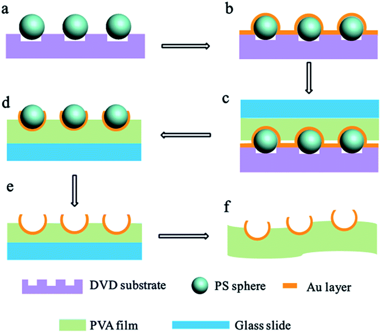 | ||
| Fig. 1 Schematic illustration of the fabrication strategy of the aligned Au nanobowl arrays. Each inset in this scheme represents the cross-section which is perpendicular to grooves on the DVD substrate, and each PS sphere in the scheme represents a chain of PS spheres in fact. (a) PS spheres' assembly on DVD grooves; (b) deposition of the Au layer onto aligned PS spheres and the DVD substrate; (c) glass slide with a thin layer of PVA coming into conformal contact with aligned PS spheres coated with the Au layer; (d) aligned PS spheres with Au coatings around were transferred onto a glass slide; (e) PS spheres were removed by dissolving in CH2Cl2 solution; (f) PVA film was peeled off from the glass slide. | ||
To obtain aligned PS sphere arrays on the grooves of the DVD substrate, a template-assisted self-assembly process was performed.41–43 First, a fluidic cell was fabricated. As shown in Fig. 2a, the fluidic cell was simply created by sandwiching a thin frame of the Mylar film between two parallel substrates. It should be noted that the bottom substrate was the DVD substrate with grooves upwards, while the top substrate was a glass slide with a small hole (ca. 2 mm in diameter) drilled on it, and then a glass tube was fixed to this hole with epoxy. Afterwards, this sandwiched structure was tightened with binder clips. Then, aqueous dispersion of PS spheres was injected into the fluidic cell through the glass tube. And the suspension was confined in the fluidic cell to make it flow slowly along the grooves. As a result, this aqueous suspension can continuously evaporate through the glass tube when it is flowing. Finally, the PS spheres can be self-assembled into the grooves on the DVD substrate when the liquid was dewetted from the bottom surface of the DVD substrate. As the meniscus slowly recedes across the substrate, PS spheres concentrate at the three-phase contact line. As shown in Fig. 2b, there were three major forces exerted on each sphere during the process, which are the capillary force associated with the meniscus of the liquid, gravitational force and electrostatic force caused by charges resting on the surfaces of the PS spheres and the substrate. Particularly, the capillary force that originates from the liquid meniscus plays the most important role in pushing PS spheres into the grooves on the DVD substrate. Furthermore, the strength of the attraction of capillary forces between adjacent spheres in the same groove is much larger than those between spheres in adjacent grooves, so all the spheres remained in the grooves with certain orientation.
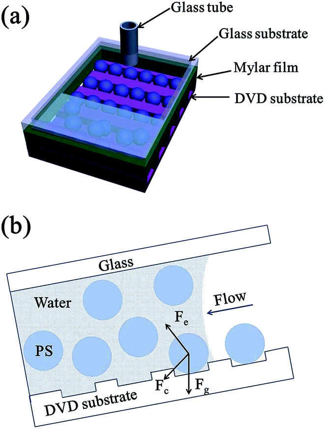 | ||
| Fig. 2 (a) A schematic illustration of the fluidic cell that was used to assemble PS spheres into grooves on the DVD substrate. (b) A cross-sectional view of the fluidic cell. For a PS sphere next to the rear edge of the colloidal suspension, there are three possible forces exerted on it: the capillary force (Fc), the gravitational force (Fg), and the electrostatic force (Fe). | ||
2.3 Characterization
The morphology of samples was observed by using a field-emission scanning electronic microscope (FESEM, Sirion 200 FEG). Optical transmission and reflection measurements in different angles of incident light were carried out with an Ideaoptics PG2000-Pro-Ex system equipped with a FIB-600-DUV optical fiber. The spectral integration time of collecting the signals was set to be 11 ms. A special support named R1 series (Ideaoptics instrument Co., LTD) with 360° rotating arms equipped with a light source and detector, and a horizontal sample stage in the center was also employed.3. Results and discussion
3.1 Morphologies and structures
Fig. 3 presents morphologies of the samples obtained in some certain steps. Fig. 3a shows the typical FESEM image of the blank DVD substrate with parallelly aligned grooves (groove width: ca. 300 nm, its depth: ca. 100 nm and its periodicity: ca. 730 nm). The PS spheres are arranged into grooves on the substrate by a template-assisted self-assembling process, forming a colloidal necklace alignment, as shown in Fig. 3b. All the PS spheres were self-assembled along the substrate grooves, yielding an array of parallel colloidal chains with a controlled preferential orientation. It is worth noting that there was little space between PS spheres in each chain, which may be because of the attraction of capillary forces and repulsion of electrostatic forces between two spheres. Additionally, because the width of grooves was ca. 300 nm, and the depth was ca. 100 nm, PS spheres with a diameter of 300 nm to 500 nm would get stuck in the groove and only a string of PS spheres could be self-assembled into the groove according to the geometrical configuration. A thin Au layer was deposited on the aligned PS sphere chain array with its substrate via plasma sputtering. Such aligned PS sphere arrays with a thin Au layer were transferred onto another glass slide which was spin coated with a thin film of PVA, as displayed in Fig. 3c. One can find that the aligned PS spheres coated with an Au layer had been successfully transferred onto the new substrate (glass slide) without obvious defects. It can be observed that spheres in one chain come closer to each other compared with ones before coating with Au layer. This was attributed to Au coating on PS spheres, decreasing the interspace between neighboring spheres. The deposited Au layer on the substrate between grooves could not contact the PVA film during the transferring process, this part of Au layer would be left on the DVD substrate when the substrate was separated from the glass slide, so the aligned PS sphere array with an Au layer at the sphere bottom remained. The aligned Au nanobowl chain is formed on the substrate after removing PS spheres by chemical dissolution, as demonstrated in Fig. 3d and e. As shown in Fig. 3d, the Au nanobowl has an open mouth on its top and it seems like a quasi-ellipsoid from the top view. The long axis of the ellipsoid was about 500 nm, the same as the diameter of the PS sphere template; nonetheless, the short axis of that was 470 nm or so, a little smaller than the diameter of the PS sphere template. This phenomenon can be explained as follows: for the direction parallel to the chains, there was a good adhesion between neighboring nanobowls due to the deposited Au layer in the preparation process. Therefore, the Au layer would not shrink much on this direction when one PS sphere was dissolved in CH2Cl2. On the other hand, for the direction perpendicular to the chains, there was no force to support the nanobowl wall, so the wall of the nanobowl at the top along the short axis would shrink slightly to the center due to the capillary force of the solvent during solvent evaporation. To summarise, Au nanobowls were upwards and parallel aligned with certain orientation and Au nanobowls in one chain were coterminal. In addition, this PVA film can be peeled off from the glass slide, aligned Au nanobowl arrays on a flexible film can be obtained through this way. As can be seen in Fig. 3f, the photograph of the as-prepared aligned Au nanobowls on the PVA film, the size of the aligned Au nanobowl arrays fabricated by this process achieved several millimeters, which is perfect for further applications.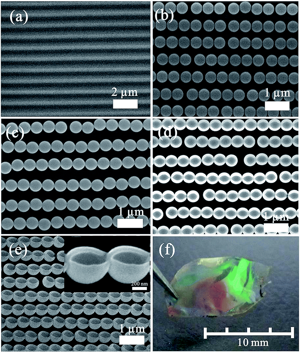 | ||
| Fig. 3 The morphologies of the samples obtained in different steps: (a) typical FESEM image of a blank DVD with aligned grooves on the inner interface; (b) FESEM image of the aligned PS sphere array on DVD grooves; (c) FESEM image of the aligned PS sphere array in (b) transferred onto the glass slide after deposition of the Au layer; (d and e) top view and 45°-tilted FESEM image of the aligned Au nanobowls. The inset in (e) is the local magnified image; (f) photograph of the as-prepared aligned Au nanobowls on a flexible PVA film. | ||
3.2 Optical transmission with anisotropy
This kind of nanostructured array with a high aspect ratio, periodicity and symmetry-reduced is likely to be sensitive to the angle of incident light. Angle-resolved transmission measurements were performed at oblique incidence for the aligned Au nanobowl arrays on a flexible PVA film, as presented in Fig. 4. Fig. 4a briefly illustrates the configuration of the angle-resolved measurements. At normal incidence the light beam makes angles α and β to be 0°. The angle of incident light relative to the sample surface was varied in two distinct ways: (1) the incident light was moving in the plane perpendicular to Au nanobowl chains, angle α changed from 0° to 30°, and the transmission light was detected underneath the sample with changing location corresponding to the incident light; (2) the incident light was moving in the plane parallel to Au nanobowl chains, angle β changed from 0° to 30°, other experimental setup was the same as (1). In the process of measuring, the prepared sample was fixed horizontally, while the light source and detector were rotated around simultaneously. And the spectra shown in Fig. 4c and d were recorded by varying the incidence angle with an interval of 2° for each measurement. A halogen lamp (wavelength from 400 nm to 1100 nm) was used as the light source.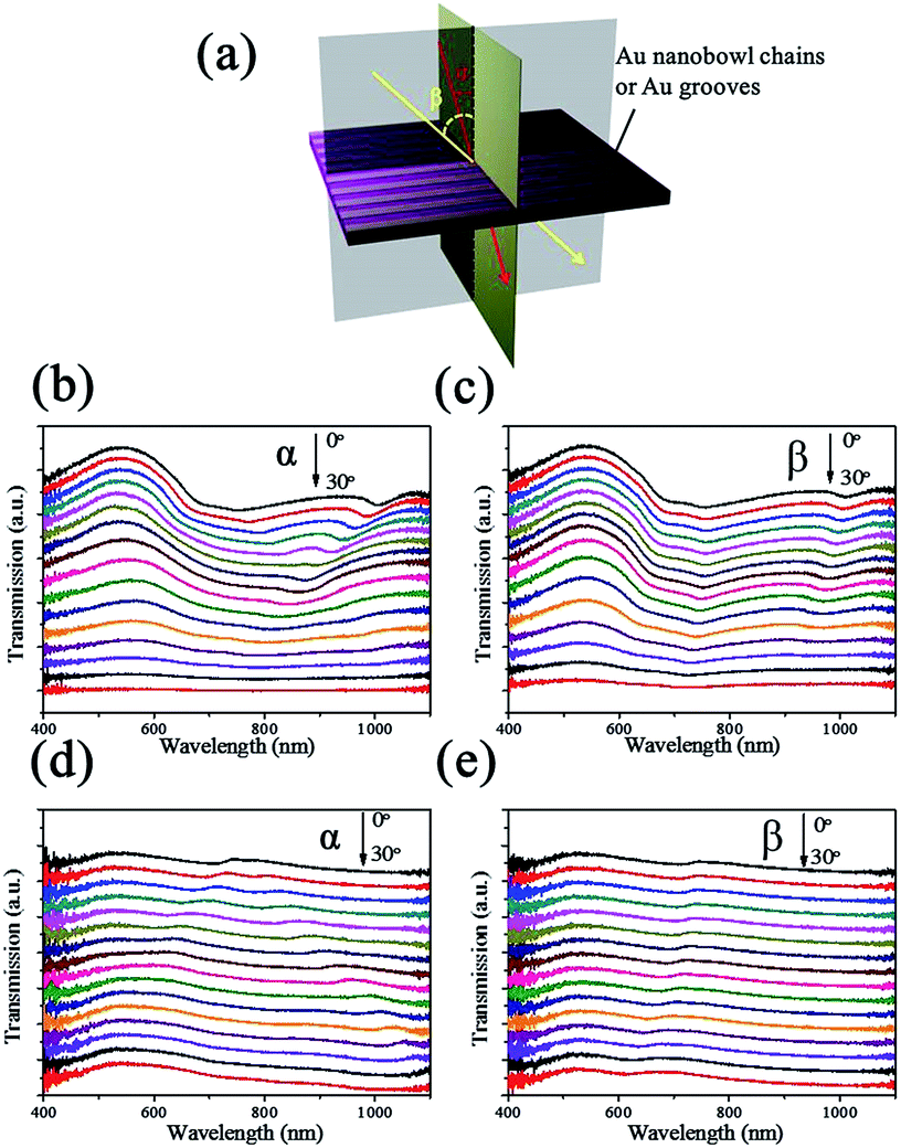 | ||
| Fig. 4 (a) Schematic outline of the configuration of the incident light relative to the linear nanostructure. (b and c) Angle-resolved transmission spectra of aligned Au nanobowl arrays. (d and e) Angle-resolved transmission spectra of Au groove arrays. | ||
The transmission spectra with changes of incidence angle are shown in Fig. 4b and c. One can see that the transmittance intensity decreased with increasing incident angle (α or β) due to a reduction in the in-plane component of the incident light wavevector perpendicular to the PVA film when α or β increased. The transmittance was relatively reduced much at a wavelength longer than 730 nm (periodicity of aligned arrays) because of the diffraction of light occurring in the region of longer wavelength. On the other hand, the strong transmission efficiency at a wavelength less than 730 nm might be caused by a good match of configuration and strong enhancement of the surface plasmon energy. For the nanobowls, surface plasmons (SPs) were excited at the two Au/air interface (inside and outside the nanobowls), resulting in surface plasmon energy matching on the two sides of nanobowls.44 Two dips were located at ca. 730 nm (refractive index of air is 1) and 1100 nm (refractive index of the PVA film is about 1.5), respectively, when α and β were fixed at 0°. And they blue-shifted when the incidence angle α or β increased. This is an exact behavior observed when light couples with SPs in reflection gratings.45,46 SPs are oscillations of surface charges at the metal interface and are excited when their momentum matches the momentum of the incident photon and the grating as follows:
| ksp = kx + kg |
![[thin space (1/6-em)]](https://www.rsc.org/images/entities/char_2009.gif) θ is the component of the incident photon's wavevector in the plane of the array (θ represents α or β, λ represents the wavelength of incident light), and kg = 2π/na is the grating momentum wavevector for the aligned array (n means the refractive index of dielectric, a means periodicity of the aligned array). In consequence, ksp would increase with the increase in α or β, leading to the transmission dip blue-shift. In addition, there was also a slight red-shift from ca. 730 nm in Fig. 4b, which may be caused by the periodic function in the direction perpendicular to the Au nanobowl chains. However, the signals were overlapped with the blue-shift signals starting from ca. 1100 nm when α increased larger enough. These preliminary results represent a motivation to carry on the study of surface plasmonic properties of this type of noble metal nanostructure. Eventually their application and fundamental scientific potential should be emphasized.
θ is the component of the incident photon's wavevector in the plane of the array (θ represents α or β, λ represents the wavelength of incident light), and kg = 2π/na is the grating momentum wavevector for the aligned array (n means the refractive index of dielectric, a means periodicity of the aligned array). In consequence, ksp would increase with the increase in α or β, leading to the transmission dip blue-shift. In addition, there was also a slight red-shift from ca. 730 nm in Fig. 4b, which may be caused by the periodic function in the direction perpendicular to the Au nanobowl chains. However, the signals were overlapped with the blue-shift signals starting from ca. 1100 nm when α increased larger enough. These preliminary results represent a motivation to carry on the study of surface plasmonic properties of this type of noble metal nanostructure. Eventually their application and fundamental scientific potential should be emphasized.
For comparison, angle-resolved transmission spectra of the DVD substrate coated with ca. 40 nm Au layer under the same conditions were recorded, as shown in Fig. 4d and e. When α and β were fixed at 0°, there was one dip at ca. 730 nm in the two spectra which was caused by SPR of Au grooves, while the dip blue-shifted when the angle α or β increased. In Fig. 5e, the shift of the dip was much more notable than that in Fig. 5f, which was caused by different periodicities in different directions of the sample. Furthermore, there was no transmission enhancement at a wavelength less than 730 nm compared with the aligned Au nanobowl arrays.
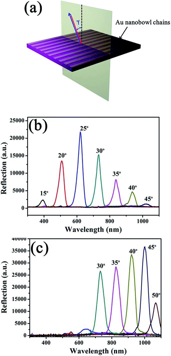 | ||
| Fig. 5 (a) Schematic outline of the configuration of the incident light relative to the grooves on the DVD substrate or the Au nanobowl linear nanostructure for measurements of reflectance spectra; (b and c) reflectance spectra of the DVD substrate and the aligned Au nanobowl arrays. | ||
3.3 Optical grating with high reflectance
The DVD substrate with aligned grooves and aligned Au nanobowl arrays can be considered as gratings. We further investigated angle-resolved reflection spectra of both a DVD substrate with aligned grooves and aligned Au nanobowl arrays. Fig. 5a schematically shows the orientation of the incident light relative to the grooves on the DVD substrate or the Au nanobowl chains for measurements of reflection spectra. As can be seen, the prepared sample was fixed horizontally, and the light source and detector were rotated at the same location simultaneously, so that backscattered light from the sample would be detected. The incident light was moving in the plane perpendicular to DVD grooves or Au nanobowl chains, and the angle γ increased from 15° to 50°. The reflection spectra were recorded by varying the incidence angle with an interval of 5° for each measurement. In this way, the diffraction peak of 2-dementional patterns can be measured.47Fig. 5b and c present angle-resolved reflection spectra of the DVD substrate with aligned grooves and aligned Au nanobowl arrays, respectively. Some fascinating phenomena can be observed from the two reflectance spectra. As can be seen in the two spectra, the peak appeared at specific angles on changing the incident light angle, and the peak continuously shifted to a longer wavelength with the increase in the incident light angle. For the DVD substrate, the peak intensity gradually increased when the incident light angle increased from 15° to 25° and then decreased thereafter. This intensity change may be caused by the combined effect of the angular dependence of the irradiated area and the reflectivity of the substrate. For aligned Au nanobowl arrays, there was no obvious signal in the spectra when the incident light angle was less than 30°. However, peaks appeared when the incident light angle increased from 30° to 50°. This phenomenon might be caused by the reasons as follows: when the incident angle was less than 30°, back-reflected light from the flat Au surface excited gap plasmons in the small gaps between the neighboring gold bowls, which were then adiabatically nanofocused in the gaps in the direction away from the surface. The gap plasmons subsequently dissipated their energy through the way of ohmic losses, leading to strong absorption. Therefore, the reflectance below 30° of the incidence angle is quite low. When the angle of incidence increased large enough, the light eventually stopped being able to excite gap plasmons via back-reflection in this configuration, and lossy adiabatic nanofocusing no longer occurred. Therefore, the optical reflection dominated on the top surface of the bowls.48 After all, regarding the peak intensity, the peaks in Fig. 5c were much stronger then those of Fig. 5b, which may be caused by two reasons as follows. On the one hand, the power in the diffraction peak is related to the amplitude of the grating.49 In this case, the depth of grooves on the DVD substrate (ca. 100 nm) and the height of Au nanobowls (ca. 400 nm) were the amplitudes. It is obvious that the amplitude of the aligned Au nanobowl arrays is greater than that of the DVD substrate. On the other hand, the intensity of the peak also directly depends on the reflective index of samples. As we all know that the reflective index of Au is much bigger than that of polycarbonate (DVD substrate). It can be concluded that the aligned Au nanobowl arrays demonstrate much stronger reflectance than general gratings in a certain wavelength region.4. Conclusions
In conclusion, we have developed a simple route with low cost to fabricate large-area aligned Au nanobowl arrays by the combination of template-assisted self-assembly and colloid lithography. Notably, this structure with a high aspect ratio configuration and symmetry-reducing units is anisotropic in optical response, which was confirmed by angle-resolved transmission measurements. Such optical anisotropy results from different LSPR modes along and across the aligned Au nanobowl chains. Additionally, the aligned Au nanobowl arrays can be used as an optical grating with higher reflectance. Owing to the special optical properties, these aligned Au nanobowl arrays have important applications in many fields of optical sensing, biological detection, and so on.Acknowledgements
The authors acknowledge the financial support from the National Basic Research Program of China (Grant no. 2012CB932303), Recruitment Program of Global Experts (C), Natural Science Foundation of China (Grant no. 51371165), Cross-disciplinary Collaborative Teams Program in CAS, and International Innovative Research Team in CAS.Notes and references
- T. Song, J. L. Xia, J. H. Lee, D. H. Lee, M. S. Kwon, J. M. Choi, J. Wu, S. K. Doo, H. Chang, W. Park, D. S. Zang, H. Kim, Y. G. Huang, K. C. Hwang, J. A. Rogers and U. Paik, Nano Lett., 2010, 10, 1710 CrossRef CAS PubMed.
- V. E. Ferry, M. A. Veerschuuren, H. B. T. Li, W. Verhagen, R. J. Walters, R. E. I. Schropp, H. A. Atwater and A. Polman, Opt. Express, 2010, 18, 237 CrossRef PubMed.
- J. W. Liu, J. Esssner and J. Li, Chem. Mater., 2010, 22, 5022 CrossRef CAS.
- W. B. Wei, K. Chen and G. L. Ge, Adv. Mater., 2013, 25, 3863 CrossRef CAS PubMed.
- X. X. Chen, H. M. Gong, S. W. Dai, D. Zhao, Y. Q. Yang, Q. Li and M. Qiu, Opt. Lett., 2013, 38(13), 2247 CrossRef PubMed.
- L. Shao, Q. F. Ruan, R. B. Jiang and J. F. Wang, Small, 2014, 10, 802 CrossRef CAS PubMed.
- A. B. D. Brown, C. G. Smith and A. R. Rennie, Phys. Rev. E: Stat. Phys., Plasmas, Fluids, Relat. Interdiscip. Top., 2000, 62, 951 CrossRef CAS.
- H. M. Lee, Y. N. Kim, B. H. Kim, S. O. Kim and W. O. Cho, Adv. Mater., 2008, 20, 2094 CrossRef CAS.
- B. D. Terris and T. Thomson, J. Phys. D: Appl. Phys., 2005, 38, 199 CrossRef.
- C. L. C. Smith, B. Desiatov, I. Goykmann, I. Fernandez-Cuesta, U. Levy and A. Kristensen, Opt. Express, 2012, 20, 5696 CrossRef PubMed.
- A. A. Tseng, J. Micromech. Microeng., 2004, 14, 15 CrossRef.
- H. Bai, C. Du, A. J. Zhang and L. Li, Angew. Chem., Int. Ed., 2013, 52, 12240 CrossRef CAS PubMed.
- A. R. Tao, J. X. Huang and P. D. Yang, Acc. Chem. Res., 2008, 41, 1662 CrossRef CAS PubMed.
- Y. Li, G. T. Duan, G. Q. Liu and W. P. Cai, Chem. Soc. Rev., 2013, 42, 3614 RSC.
- Y. Li, N. Koshizaki and W. P. Cai, Coord. Chem. Rev., 2011, 255, 357 CrossRef CAS PubMed.
- Z. F. Dai, L. C. Jia, G. T. Duan, Y. Li, H. W. Zhang, J. J. Wang, J. L. Hu and W. P. Cai, Chem.–Eur. J., 2013, 19, 13387 CrossRef CAS PubMed.
- D. Babonneau, S. Camelio, L. Simonot, F. Pailloux, P. Guérin, B. Lamongie and O. Lyon, EPL, 2011, 93, 26005 CrossRef.
- T. W. H. Oates, M. Ranjan, S. Facsko and H. Arwin, Opt. Express, 2011, 19, 2014 CrossRef CAS PubMed.
- M. Ranjan, T. W. H. Oates, S. Facsko and W. Möller, Opt. Lett., 2010, 35, 2576 CrossRef CAS PubMed.
- R. Verre, K. Fleischer, O. Ualibek and I. V. Shvets, Appl. Phys. Lett., 2012, 100, 031102 CrossRef PubMed.
- T. W. H. Oates, A. Keller, S. Facsko and A. Mücklich, Plasmonics, 2007, 2, 47 CrossRef CAS.
- A. Toma, D. Chiappe, D. Massabo, C. Boragno and F. B. Mongeot, Appl. Phys. Lett., 2008, 93, 163104 CrossRef PubMed.
- O. M. Liedke, B. Liedke, A. Keller, B. Hillebrands, A. Mucklich, S. Facsko and J. Fassbender, Phys. Rev. B: Condens. Matter Mater. Phys., 2007, 75, 220407 CrossRef.
- M. Ranjan, S. Fascko, M. Fritzsche and S. Mukherjee, Microelectron. Eng., 2013, 102, 44 CrossRef CAS PubMed.
- M. Ranjan, J. Nanopart. Res., 2013, 15, 1908 CrossRef.
- P. Albella, B. Garcia-Cueto, F. González, F. Moreno, P. C. Wu, T. H. Kim, A. Brown, Y. Yang, H. O. Everitt and G. Vidden, Nano Lett., 2011, 11, 3531 CrossRef CAS PubMed.
- M. A. Mahmoud and M. A. El-sayed, J. Am. Chem. Soc., 2010, 132, 12704 CrossRef CAS PubMed.
- H. Q. Wang, L. C. Jia, L. Li, Z. Swiatkowska-Warkocka, K. Kawaguchi, A. Pyatenko and N. Koshizaki, J. Mater. Chem. A, 2013, 1, 692 CAS.
- M. Gkikas, J. Timonen, J. Ruokolainen, P. Alexandridis and H. Iatrou, J. Polym. Sci., Part A: Polym. Chem., 2013, 51, 1448 CrossRef CAS.
- P. Y. Lim, R. S. Liu, P. L. She, C. F. Hung and H. C. Shih, Chem. Phys. Lett., 2006, 420, 304 CrossRef CAS PubMed.
- Y. Li, C. C. Li, S. O. Cho, G. T. Duan and W. P. Cai, Langmuir, 2007, 23, 9802 CrossRef CAS PubMed.
- J. Ye, P. V. Dorpe, W. V. Roy, G. Borghs and G. Maes, Langmuir, 2009, 25, 1822 CrossRef CAS PubMed.
- C. T. Cooper, M. Rodriguez, S. Blair and J. S. Shumaker-Parry, J. Phys. Chem. C, 2014, 118, 1167 CAS.
- C. C. Kei, T. H. Chen, C. M. Chang, C. Y. Su, C. T. Lee, C. N. Hsiao, S. C. Chang and T. P. Perng, Chem. Mater., 2007, 19, 5833 CrossRef CAS.
- M. G. Banaee and K. B. Crozier, Opt. Lett., 2010, 35, 760 CrossRef CAS PubMed.
- K. L. Hobbs, P. R. Larson, G. D. Lian, J. C. Keay and M. B. Johnson, Nano Lett., 2004, 4, 167 CrossRef CAS.
- C. Charnay, A. Lee, S. Man, C. E. Moran, C. Radloff, R. K. Bradley and N. Halas, J. Phys. Chem. B, 2003, 107, 7327 CrossRef CAS.
- M. Cortie and M. Ford, Nanotechnology, 2007, 18, 235704 CrossRef.
- J. Ye, P. V. Dorpe, W. V. Roy, K. Lodewijks, I. D. Vlaminck, G. Maes and G. Borghs, J. Phys. Chem. C, 2009, 113, 3110 CAS.
- J. Ye, P. V. Dorpe, W. V. Roy, G. Borghs and G. Maes, Langmuir, 2009, 25, 1822 CrossRef CAS PubMed.
- Y. D. Yin, Y. Lu, B. Gates and Y. N. Xia, J. Am. Chem. Soc., 2001, 123, 8718 CrossRef CAS PubMed.
- Y. D. Yin, Y. Lu and Y. N. Xia, J. Am. Chem. Soc., 2001, 123, 771 CrossRef CAS.
- Y. N. Xia, Y. D. Yin, Y. Lu and J. McLellan, Adv. Funct. Mater., 2003, 13, 907 CrossRef CAS.
- B. Ai, Y. Yu, H. Mohwald and G. Zhang, Nanotechnology, 2013, 24, 035303 CrossRef PubMed.
- R. H. Ritchie, E. T. Arakawa, J. J. Cowan and R. N. Hamm, Phys. Rev. Lett., 1968, 21, 1530 CrossRef CAS.
- T. W. Ebbesen, H. J. Lezec, H. F. Ghaemi, T. Thio and P. A. Wolff, Nature, 1998, 391, 667 CrossRef CAS PubMed.
- T. Kanai, T. Sawada and K. Kitamura, Langmuir, 2003, 19, 1984 CrossRef CAS.
- T. Søndergaard, S. M. Novikov, T. Holmgaard, R. L. Eriksen, J. Beermann, Z. Han, K. Pedersen and S. I. Bozhevolnyi, Nat. Commun., 2012, 3, 969 CrossRef PubMed.
- E. Marx, T. A. Germer, T. V. Vorburger and B. C. Park, Appl. Opt., 2000, 39, 4473 CrossRef CAS.
| This journal is © The Royal Society of Chemistry 2015 |