
 Open Access Article
 This Open Access Article is licensed under a
 Creative Commons Attribution 3.0 Unported Licence
High-performance deformable photoswitches with p-doped graphene as the top window electrode†
Rongjin
Li
a,
Zhaoyang
Liu
a,
Khaled
Parvez
a,
Xinliang
Feng
*ab and
Klaus
Müllen
*a
aMax Planck Institute for Polymer Research, Ackermannweg 10, Mainz 55128, Germany. E-mail: feng@mpip-mainz.mpg.de; muellen@mpip-mainz.mpg.de; Fax: +49 6131 379 350; Tel: +49 6131 379 150
bTechnische Universitaet Dresden, 01062 Dresden, Germany. Tel: +49 351 463 43250
First published on 6th November 2014
Abstract
Deformable polymer photoswitches with p-doped single layer graphene as the top window electrode exhibit excellent photoresponse with an on/off ratio as high as 8.5 × 10⁵. The charge-transfer doping of graphene results in better charge separation and collection efficiency and the structure of the top electrode minimizes the dark current.
Photoswitches are widely used for numerous applications, including environmental monitoring, optoelectronic circuits and remote control.1–5 To be ideal photoswitches, they should exhibit high on/off ratio (ratio of photocurrent to dark current) and low energy consumption.6 To meet the requirements of the next generation organic optoelectronic circuits, they should also be flexible and light-weight. While optoelectronic devices made of inorganic materials (such as a-Si:H) are widely used, they are relatively brittle and heavy. Organic photosensitive polymers are good candidates for constructing flexible polymer photoswitches since they are inherently flexible compared to their inorganic counterparts. Furthermore, they have advantages such as compatibility with low-cost solution processing for large-area detection, a wide selection of materials, and being light-weight. In general, there are two types of photoswitches based on polymers, i.e. photodiodes in which the photosensitive materials are bulk heterojunction blends of electron donors (D) and acceptors (A) [such as a blend of poly(3-hexylthiophene) (P3HT) and [6,6]-phenyl C61-butyric acid methyl ester (PCBM)], and photoconductors, which are electrically conductive polymers that become more conductive due to the absorption of light radiation. Photodiodes have several advantages over photoconductors, e.g., they are self-powered (working in the photovoltaic mode) and have a reduced electron–hole recombination (formation of a built-in electric field).2,7 Photodiodes exhibit a much higher photoresponse speed and higher photosensitivity than photoconductors.8
Photodiodes are typically fabricated with a sandwich geometry having two electrodes with different work function (WF) and at least one of them being transparent (the window electrode).2,9 The transparent electrode acts as both a window for light to pass through to the photosensitive material and an Ohmic contact for charge carrier collection. Indium tin oxide (ITO), as the most widely used window electrode material in optoelectronic devices,2,3,9–15 is however inherently brittle, which makes it unsuitable for flexible devices. Moreover, ITO is a toxic material with the potential to generate high amounts of reactive oxygen species and is thus a biohazard.16 Recently, graphene has emerged as an attractive alternative because of its outstanding electronic, optoelectronic, and mechanical properties.17 Although graphene shows excellent flexibility18 and high transmittance in the visible range19 coupled with low sheet resistance (RS),20 the use of graphene as top window electrodes for flexible optoelectronic devices has rarely been investigated.21
In this work, we report the first deformable organic polymer photoswitch arrays with p-doped single layer graphene (SLG) as the top window electrode. An electron-withdrawing fluoropolymer, poly(vinylidene fluoride-co-hexafluoropropene) (PVDF-HFP), is used to transfer and simultaneously dope the chemical vapor deposition (CVD)-grown SLG. The p-doping induced by the fluoropolymer not only decreases the RS, but also increases the WF of graphene for better charge separation and collection. Photoswitches were fabricated using p-doped SLG as the top window electrode, which avoids the deposition of metal on the photosensitive polymer and minimizes the dark current. Remarkably, the fabricated photoswitches show a high on/off ratio up to 8.5 × 10⁵, which is the highest value for organic photoswitches reported so far,6,7 indicating the excellent performance of the device. Moreover, the fabricated photoswitches with graphene anodes are flexible and can be bent or even crumpled, demonstrating their high potential in stretchable electronics.22
Single layer graphene was produced by chemical vapor deposition on a copper foil and transferred to the target substrates by a thin poly(methyl methacrylate) (PMMA, denoted hereafter as G) or PVDF-HFP (denoted hereafter as FG) film. PVDF-HFP was selected as the p-dopant due to its electron-deficient nature, excellent film formation properties and high tensile strength.23 Inorganic substances such as AuCl3 or HNO3 were commonly used as p-dopants for graphene. However, doping by these materials was unstable due to either the hygroscopic effect or the volatile nature of the dopant.24,25 In contrast, PVDF-HFP doped graphene films are stable and the change of RS is less than 5% over a period of 2 months (Fig. S1, ESI†).
Raman spectroscopy was firstly employed to investigate the electronic structure of both graphene films. Compared to G, FG exhibited a marked decrease of the intensity ratio of the 2D to G peak (I2D/IG) from 3.4 to 1.9, and a decrease of the full-width at half maximum of the G band from 33.3 to 27.2 cm−1 in the Raman spectra.26 The blue shift of both the G and 2D frequencies (9.5 and 20.5 cm−1 for the G and 2D peaks, respectively) further confirmed the p-doping effect (Fig. 1a).26,27 The doping was ascribed to the dipoles formed at the interface as a consequence of electron transfer from the π-bonding levels of graphene near the Dirac point to the lowest unoccupied molecular orbital (LUMO) of the dopant (PVDF-HFP).28–32 Based on the shift of the G peak (9.5 cm−1), a decrease of the Fermi level of ∼0.2 eV is estimated.27 Due to the effective p-doping (i.e., the move of the Fermi level away from the Dirac point), the RS significantly decreased from 425 Ω sq−1 (G) to 256 Ω sq−1 (FG, ∼40% reduction, Fig. 1b). Nevertheless, the transmittance of the FG was decreased by only 1.2% compared to that of the G (Fig. 1c). Moreover, the work function of a G film determined by ultraviolet photoelectron spectroscopy (UPS) was 4.34 eV and this value increased to 4.56 eV after doping (Fig. 1d). Considering that graphene is a zero-gap semiconductor, the increase of the work function (0.21 eV) coincides with the decrease of the Fermi level determined by Raman spectroscopy (∼0.2 eV). The decreased RS and increased WF render FG a good candidate as anodes for the fabrication of photoswitches.
 | ||
| Fig. 1 (a) Raman spectra (the inset shows the chemical structures of PVDF-HFP and PMMA), (b) sheet resistance, (c) transmittance, and (d) UPS spectra of G and FG films on a polyethylene naphthalate (PEN) substrate. | ||
Encouraged by the enhanced electronic properties of FG, we next applied the graphene films as the window electrode for the fabrication of flexible photoswitches. The main procedures are shown in Fig. S2 (ESI†). First, SLG on Cu foil was patterned with a shadow mask using a previously described method33 (Fig. S2a and b†). Subsequently, a PVDF-HFP or PMMA solution was spin-coated on the pattern and the Cu foil was etched away using a Fe(NO3)3 aqueous solution (Fig. S2c†). Al bottom electrodes (60 nm thick) were deposited onto polyethylene naphthalate (PEN) or polyethylene terephthalate (PET) substrates with the same shadow mask and the photosensitive polymer layer (blend of P3HT:PCBM) was spin-coated on top of the Al bottom electrodes (Fig. S2d and e†). Finally, PVDF-HFP or PMMA-supported graphene patterns were positioned on top of the PEN or PET substrate and vertically aligned with the bottom Al electrodes (Fig. S2f†). Thus, photoswitches with 8 × 8 arrays were built up with a sandwich structure of substrate/Al/P3HT:PCBM/SLG (Fig. 2a). Fig. 2b and c show photographs of the devices in flat and bent states.
 | ||
| Fig. 2 Schematic structure and photoresponse of photoswitches based on G and FG top window electrodes. (a) Sketch of the structure of the photoswitches with graphene as the top window electrode. (b and c) Photographs of the photoswitches in flat and bent states. (c) J–V characteristics of G-photoswitch and FG-photoswitch. (d) Photoresponse of a FG-photoswitch. | ||
Typical current–voltage (J–V) characteristics of the photoswitches with G (G-photoswitch) and FG (FG-photoswitch) as the top window electrodes are presented in Fig. 2d. The curves moved far away from the origin (0,0), which is indicative of the photovoltaic effect.34 Both G-photoswitch and FG-photoswitch had a similar open-circuit voltage (VOC) of ∼0.44 V. Remarkably, the FG-photoswitch exhibited a short-circuit current (JSC) of 1.9 mA cm−2, which was 72% higher than that of the G-photoswitch (1.1 mA cm−2). The increased JSC was ascribed to the increased WF and decreased RS of FG, which facilitated charge separation and collection. Taking advantage of the photovoltaic effect, the FG-photoswitches could work at 0 V bias, meaning that photons could be detected without an external energy supply. Fig. 2e shows the photoresponse of FG-photoswitches at 0 V bias. The current density of the devices was lower than 10−5 mA cm−2 in the dark, whereas it jumped sharply by more than five orders of magnitude upon light irradiation (ca. 20 mW cm−2). When the light was switched on and off, the devices responded to the light and exhibited two states: a “high” current state under illumination (Jph) and a “low” current state in the dark (Jd). Thus, an on/off ratio (Jph/Jd) as high as 8.5 × 10⁵ was achieved. By comparison, the G-photoswitch exhibited a lower on/off ratio of 1.2 × 10⁵ (Fig. S3, ESI†).
The prominent photoresponse behaviour of FG-photoswitches can be ascribed to two primary features. First, the use of a FG anode results in high charge separation efficiency, and thus high photocurrent (Jph). By p-doping, the increased WF of the anode results in a larger built-in electric field (determined by the WF difference between the anode and the cathode), which is more efficient for the separation of photoinduced charges at the D–A interface.35 Without a built-in field, there will be no incentive for the carriers to drift and electrons and holes dissociated at the D–A interfaces would diffuse. When a built-in electric field is formed, the separated charge carriers will move directionally, with electrons moving to the cathode and holes moving to the anode. The increased WF of the anode (from G to FG) will create a larger built-in electric field (Fig. 3a and b), thus leading to higher efficiency for charge separation. Moreover, the increased WF of FG results in better alignment of the anode work function with respect to the donor. To form a desired Ohmic contact and effectively collect holes at the anode, the WF of the anode must be approximately equal to the HOMO of the donor. With FG as the anode, the WF is closer to the HOMO of P3HT (5.0 eV) than that of G (4.34 eV) and thus a better hole collection efficiency is expected. Second, the dark current (Jd) is reduced by using a transferred top graphene electrode. The device has a structure of substrate/Al/P3HT:PCBM/FG. The FG window electrode is transferred on top of the photosensitive polymer; thus the direct deposition of metal on the polymer layer is avoided. For comparison, we also fabricated devices with a structure of substrate/FG/P3HT:PCBM/Al, in which the Al layer was thermally evaporated on top of the polymer layer. The dark current of such a device was on the order of 10−3 mA cm−2 (Fig. 3c), which was nearly three orders of magnitude higher than that with graphene as the top electrode. Although the photocurrent increased (3.6 fold), the on/off ratio decreased to 4.4 × 10³ (Fig. 3c and d). The increased dark current can be attributed to the diffusion of metal atoms into the polymer layer, which tends to form clusters on or below the surface of the polymer.36–38
 | ||
| Fig. 3 (a and b) Simple energy level diagrams of the photoswitches using G or FG as the window electrode in the short circuit mode. (c) Photoresponse of devices with evaporated aluminium as the top electrode. (d) Comparison of the photoresponse of photoswitches with both top graphene and top aluminium electrodes. | ||
We further examined the bendability of the photoswitches with p-doped graphene as the top window electrode. Even after 900 cycles of repeated bending of the FG-photoswitches (on a 175 µm thick PEN film) to a radius of ∼6 mm, there was little change in the photoresponse (Fig. S4, ESI†). For applications in wearable electronics, the devices need to be both bendable and deformable.22 Thus, we also fabricated FG-photoswitches on 2.5 µm thick PET films to afford devices with a total thickness of less than 2.7 µm. The ultrathin devices were lightweight (1.6 mg for an 8 × 8 array) and exhibited extremely good flexibility. To further evaluate the photoresponse stability after deformation, the devices were crumpled into a ball of ∼5 mm diameter and then flattened (Fig. 4a–c). The radius of curvature of the wrinkles was estimated to be several tens of micrometers (Fig. 4d). Remarkably, the devices could still perform as photoswitches and the photoresponse behaviour was only slightly changed (Fig. 4e). The mean on/off ratio of nine randomly selected devices decreased by less than 10% after the deformation (Fig. S5, ESI†), highlighting the outstanding flexibility of the photoswitches and their robustness to mechanical deformation.
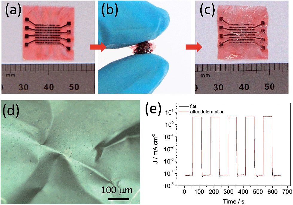 | ||
| Fig. 4 Deformable photoswitches. (a–c) Photographs of a flat, crumpled, and flattened device. (d) Optical micrograph of the PET surface of the photoswitch being crumpled and flattened. (e) A typical photoresponse curve before and after deformation. | ||
Conclusions
In summary, we developed the first deformable polymer photoswitch arrays with PVDF-HFP doped SLG as the top window electrode. The introduction of p-doped graphene facilitated the charge separation and collection, and the structure of the transferred top window electrode avoided the diffusion of metal into the polymer and minimized the dark current. This resulted in a high on/off ratio of 8.5 × 10⁵. The device structure developed in this study provides an inexpensive but efficient method of fabricating high-performance flexible photoswitches as well as other ITO-free flexible optoelectronic devices, such as organic light-emitting diodes or organic photovoltaic cells.Acknowledgements
This work was financially supported by ERC grants on NANOGRAPH and 2DMATER, DFG Priority Program SPP 1459, EU Projects GENIUS, UPGRADE and MoQuaS, EC under Graphene Flagship (no. CNECT-ICT-604391), and support from Cfaed of TU Dresden. The authors thank Dr Ye Zou (Institute of Chemistry, Chinese Academy of Sciences) for the XPS and UPS measurements.Notes and references
- H. Dong, H. Zhu, Q. Meng, X. Gong and W. Hu, Chem. Soc. Rev., 2012, 41, 1754 RSC.
- G. Konstantatos and E. H. Sargent, Nat. Nanotechnol., 2010, 5, 391 CrossRef CAS PubMed.
- X. Gong, M. Tong, Y. Xia, W. Cai, J. S. Moon, Y. Cao, G. Yu, C.-L. Shieh, B. Nilsson and A. J. Heeger, Science, 2009, 325, 1665 CrossRef CAS PubMed.
- Q. X. Tang, L. Q. Li, Y. B. Song, Y. L. Liu, H. X. Li, W. Xu, Y. Q. Liu, W. P. Hu and D. B. Zhu, Adv. Mater., 2007, 19, 2624 CrossRef CAS.
- G. Konstantatos, I. Howard, A. Fischer, S. Hoogland, J. Clifford, E. Klem, L. Levina and E. H. Sargent, Nature, 2006, 442, 180 CrossRef CAS PubMed.
- H. Zhu, T. Li, Y. Zhang, H. Dong, J. Song, H. Zhao, Z. Wei, W. Xu, W. Hu and Z. Bo, Adv. Mater., 2010, 22, 1645 CrossRef CAS PubMed.
- S. Pang, S. Yang, X. Feng and K. Müllen, Adv. Mater., 2012, 24, 1566 CrossRef CAS PubMed.
- L. Peng, L. Hu and X. Fang, Adv. Mater., 2013, 25, 5321 CrossRef CAS PubMed.
- T. Rauch, M. Boberl, S. F. Tedde, J. Furst, M. V. Kovalenko, G. Hesser, U. Lemmer, W. Heiss and O. Hayden, Nat. Photonics, 2009, 3, 332 CrossRef CAS.
- G. Yu, J. Wang, J. McElvain and A. J. Heeger, Adv. Mater., 1998, 10, 1431 CrossRef CAS.
- P. Peumans, V. Bulovic and S. R. Forrest, Appl. Phys. Lett., 2000, 76, 3855 CrossRef CAS PubMed.
- Y. Yao, Y. Liang, V. Shrotriya, S. Xiao, L. Yu and Y. Yang, Adv. Mater., 2007, 19, 3979 CrossRef CAS.
- X. Gong, M.-H. Tong, S. H. Park, M. Liu, A. Jen and A. J. Heeger, Sensors, 2010, 10, 6488 CrossRef CAS PubMed.
- F. Guo, B. Yang, Y. Yuan, Z. Xiao, Q. Dong, Y. Bi and J. Huang, Nat. Nanotechnol., 2012, 7, 798 CrossRef CAS PubMed.
- F. Guo, Z. Xiao and J. Huang, Adv. Opt. Mater., 2013, 1, 289 CrossRef.
- D. Lison, J. Laloy, I. Corazzari, J. Muller, V. Rabolli, N. Panin, F. Huaux, I. Fenoglio and B. Fubini, Toxicol. Sci., 2009, 108, 472 CrossRef CAS PubMed.
- A. K. Geim and K. S. Novoselov, Nat. Mater., 2007, 6, 183 CrossRef CAS PubMed.
- K. S. Kim, Y. Zhao, H. Jang, S. Y. Lee, J. M. Kim, J. H. Ahn, P. Kim, J. Y. Choi and B. H. Hong, Nature, 2009, 457, 706 CrossRef CAS PubMed.
- F. Bonaccorso, Z. Sun, T. Hasan and A. C. Ferrari, Nat. Photonics, 2010, 4, 611 CrossRef CAS.
- S. Bae, H. Kim, Y. Lee, X. Xu, J.-S. Park, Y. Zheng, J. Balakrishnan, T. Lei, H. Ri Kim, Y. I. Song, Y.-J. Kim, K. S. Kim, B. Ozyilmaz, J.-H. Ahn, B. H. Hong and S. Iijima, Nat. Nanotechnol., 2010, 5, 574 CrossRef CAS PubMed.
- Z. Liu, J. Li and F. Yan, Adv. Mater., 2013, 25, 4296 CrossRef CAS PubMed.
- T. Someya, Stretchable Electronics, Wiley-VCH, Weinheim, Germany, 2013 Search PubMed.
- K. H. Lee, M. S. Kang, S. Zhang, Y. Gu, T. P. Lodge and C. D. Frisbie, Adv. Mater., 2012, 24, 4457 CrossRef CAS PubMed.
- I. H. Lee, U. J. Kim, H. B. Son, S.-M. Yoon, F. Yao, W. J. Yu, D. L. Duong, J.-Y. Choi, J. M. Kim, E. H. Lee and Y. H. Lee, J. Phys. Chem. C, 2010, 114, 11618 CAS.
- G. Jo, M. Choe, S. Lee, W. Park, Y. H. Kahng and T. Lee, Nanotechnology, 2012, 23, 112001 CrossRef PubMed.
- X. Dong, D. Fu, W. Fang, Y. Shi, P. Chen and L.-J. Li, Small, 2009, 5, 1422 CrossRef CAS PubMed.
- A. Das, S. Pisana, B. Chakraborty, S. Piscanec, S. K. Saha, U. V. Waghmare, K. S. Novoselov, H. R. Krishnamurthy, A. K. Geim, A. C. Ferrari and A. K. Sood, Nat. Nanotechnol., 2008, 3, 210 CrossRef CAS PubMed.
- W. Chen, S. Chen, D. C. Qi, X. Y. Gao and A. T. S. Wee, J. Am. Chem. Soc., 2007, 129, 10418 CrossRef CAS PubMed.
- T. Wehling, K. Novoselov, S. Morozov, E. Vdovin, M. Katsnelson, A. Geim and A. Lichtenstein, Nano Lett., 2008, 8, 173 CrossRef CAS PubMed.
- H. Pinto, R. Jones, J. P. Goss and P. R. Briddon, J. Phys.: Condens. Matter, 2009, 21, 402001 CrossRef CAS PubMed.
- H. Medina, Y.-C. Lin, D. Obergfell and P.-W. Chiu, Adv. Funct. Mater., 2011, 21, 2687 CrossRef CAS.
- A. C. Crowther, A. Ghassaei, N. Jung and L. E. Brus, ACS Nano, 2012, 6, 1865 CrossRef CAS PubMed.
- S. P. Pang, H. N. Tsao, X. L. Feng and K. Müllen, Adv. Mater., 2009, 21, 3488 CrossRef CAS.
- S. J. Fonash, Solar Cell Device Physics, Academic Press, Burlington, USA, 2nd edn, 2010 Search PubMed.
- A. W. Hains, Z. Liang, M. A. Woodhouse and B. A. Gregg, Chem. Rev., 2010, 110, 6689 CrossRef CAS PubMed.
- F. Faupel, R. Willecke and A. Thran, Mater. Sci. Eng., R, 1998, 22, 1 CrossRef.
- J. Zhu, P. Goetsch, N. Ruzycki and C. T. Campbell, J. Am. Chem. Soc., 2007, 129, 6432 CrossRef CAS PubMed.
- F. Bebensee, J. Zhu, J. H. Baricuatro, J. A. Farmer, Y. Bai, H.-P. Steinrück, C. T. Campbell and J. M. Gottfried, Langmuir, 2010, 26, 9632 CrossRef CAS PubMed.
Footnote |
| † Electronic supplementary information (ESI) available. See DOI: 10.1039/c4tc02197e |
| This journal is © The Royal Society of Chemistry 2015 |