
Nanoscale characterisation and magnetic properties of Co81Cu19/Cu multilayer nanowires†
Junwei
Zhang
a,
Hongbin
Ma
a,
Senfu
Zhang
a,
Hong
Zhang
a,
Xia
Deng
a,
Qianqian
Lan
a,
Desheng
Xue
a,
Feiming
Bai
b,
Nigel J.
Mellors
c and
Yong
Peng
*a
aKey Laboratory for Magnetism and Magnetic Materials of the Ministry of Education, Lanzhou University, Lanzhou 730000, China. E-mail: pengy@lzu.edu.cn; Tel: +86-931-8912425
bState Key Laboratory of Electronic Thin Films and Integrated Devices, University of Electronic Science and Technology, Chengdu 610054, China
cNano Materials Group, School of Computing, Science and Engineering, University of Salford, Greater Manchester M5 4WT, UK
First published on 20th October 2014
Abstract
Bamboo-like CoCu/Cu multilayer nanowires have been successfully fabricated into anodic aluminium oxide templates using an electrodeposition method, and their chemistry and crystal structure have been characterised at the nanoscale. Energy-dispersive X-ray analysis indicated that the chemical composition of the regular periodic CoCu/Cu nanowires was Co81Cu19/Cu. Diffraction analysis revealed that Cu layers and Co-rich layers exhibited polycrystalline fcc structures. A twin relationship of Cu layer {111} planes stacking on Co81Cu19 layer {111} planes was observed at the lattice-resolution level. The magnetic properties analysed by experimental and theoretical simulations showed that there was a transition from a curling rotation mode to coherent rotation mode in our Co81Cu19/Cu multilayer nanowires when the angle between external field and nanowire length axis increased from 0° to 90°. This study highlights the basic morphological, chemical, structural information and magnetic reversal mechanism of CoCu/Cu nanowires, which are critical for the applications of multilayer nanowires in nanoscale sensors and electronics.
1 Introduction
One dimensional magnetic multilayer nanowires (MNWs) with giant magnetoresistance (GMR) effects have attracted numerous interests because of their unique physical properties1,2 and potential applications in high-density magnetic recording,3 magnetic sensors4 and spin electronics5 for almost two decades.6 The origin of the interest can be traced back to 1988 when A. Fert and co-workers discovered the GMR effect in a Fe/Cr/Fe magnetic multilayer structure.7 The effect is based on the dependence of electron scattering on the spin orientation, which is observed as a significant change in the electrical resistance depending on whether the magnetisation of adjacent ferromagnetic layers are in a parallel or an anti-parallel alignment.8 The GMR effect was quickly applied to reading heads in hard disk drives, magnetic sensors and nonvolatile memories. New applications of GMR sensors are daily being exploited because of the limitations of size, weight, power consumption, and cost in the current technologies. Magnetic/nonmagnetic multilayer nanowires, as a group of important GMR materials, have always received considerable attention not only because of their potential multifunctional applications,9,10 but also from a fundamental point of view such as spin-transport mechanisms11 and magnetisation reversal processes in magnetism.12Electrodeposition methods based on anodised aluminium oxide (AAO) templates or ion-track etched polycarbonate (PC) membranes13–15 is a common technique to prepare magnetic multilayer nanowires. Diverse multilayer nanowires have been experimentally synthesized.5,16–25 Most work has focused on their morphological, magnetic and GMR properties.26,27 There is a little study on the magnetisation reversal mechanism and the nanoscale characterisation including detailed morphological, chemical, structural analysis of these multilayer nanowires.28 However, these structural characteristics are intrinsically important for their other properties affecting the coercivity, magnetisation, magnetic domain structure, magnetisation reversal mechanism and resistance characteristics of the materials.29 The magnetization reversal mechanism is essential to understand their magnetic behaviour and GMR effect and wisely design them for particular applications. Therefore, it is important to analyse the microstructure, chemistry and magnetization reversal mechanism of multilayer nanowires at the nanoscale to further understand their magnetic, GMR and other properties.
One-dimensional (1D) and two-dimensional (2D) Co–Cu multilayer structures in particular have been intensively studied because of the large GMR values at either room temperature or low temperature.5,16–18,22,26,27 Properties such as the GMR effect and magnetic anisotropy are found to be very sensitive to the morphology, structure, chemistry and grain size of individual magnetic and non-magnetic layers. In addition, the performance of Co–Cu multilayer structures prepared by an electrodeposition (ED) method16–18,22 is worse than that of those prepared by a physical deposition (PD) method.26,27 A number of published works were devoted to figure out the intrinsic reasons between the GMR effect, magnetic properties of PD Co–Cu multilayer structures and their nanoscale characterisation, including morphology, chemistry, structure, interfaces and grain sizes.26,27 However, the systemic nanoscale characterisation of 1D ED Co–Cu multilayer structures and the understanding of how their nanoscale characterisation cause a poor performance of their GMR effect and magnetic properties are sparse.18
In this work, we have carried out a detailed nanoscale characterisation of CoCu/Cu multilayer nanowires prepared by electrodeposition into AAO templates following our recent investigation.28 To the best of our knowledge, the crystal structure of Co81Cu19 alloy is believed to be determined for the first time. A twin relationship between Cu {111} planes and Co81Cu19 {111} planes stacking on each other has also been observed, which directly confirms the theoretical prediction that an error rotates the fcc crystal by 180° about <111>, forming a twin because the {111} planes of the fcc structure are not the mirror planes of the space group. This observation is believed to reveal the intrinsic reason why the GMR effect of the specimens prepared by ED method is universally smaller than those prepared by PD methods. Moreover, the magnetic properties of the multilayer nanowires have been experimentally characterised and theoretically simulated by computational micromagnetism, which further progresses our previous report.28
2 Experimental
CoCu/Cu multilayer nanowires were synthesised by electrochemical deposition into anodic alumina templates (AAO) with 40 nm diameter pores. The preparation of AAO templates is the same as our previous reports.24,30,31 A gold layer was sputtered onto one side of the template to serve as the working electrode in a standard three-electrode electrochemical cell. The reference electrode was a saturated calomel electrode (SCE) and the counter electrode was a graphite rod. The electrodeposition electrolyte was composed of 0.5 mol L−1 CoSO4·7H2O, 0.005 mol L−1 CuSO4·7H2O and 0.6 mol L−1 H3BO3. Voltammetric experiments were performed to determine the optimal electrodeposition potentials for CoCu and Cu layers (Fig. 1a). It can be observed that there was a limited current region between −0.1 V and −0.7 V, which indicated a Cu electrodeposition. The relevant small current was due to the small concentration of Cu2+ in the electrolyte. The onset of Co deposition occurred at about −0.9 V, which was followed by a sharp increase in current. Therefore, the electrodeposition potential was alternately pulsed between a constant −0.65 V for 30 s to deposit only Cu and −1.2 V for 6 s to deposit CoCu alloy. The total deposition time for each specimen was 4000 s. The electrodeposition electrolyte was continuously agitated throughout using a magnetic stirrer. Typical curves showing the time dependence of the applied cathode potential and the corresponding observed current density during the deposition of CoCu/Cu multilayer nanowires are shown in Fig. 1b. The entire electrodeposition process is similar to other multilayer nanowires in our previous reports.24,30,31 | ||
| Fig. 1 (a) Cyclic voltammetry recorded from a Co–Cu electrolytic solution used for an electrodeposition of multilayer CoCu/Cu nanowries. (b) Typical curves of time dependence of the applied deposition potential versus SCE (blue line) and observed current density (red line) during the growth of CoCu/Cu multilayer nanowires. | ||
The morphology and chemistry of the electrodeposited multilayer nanowires were analysed using a scanning electron microscope (SEM, Tescan MIRA 3) and a high-resolution transmission electron microscope (HRTEM, FEI Tecnai G2 F30 operated at 300 kV) equipped with an energy-dispersive X-ray analyzer (EDX, AMETEK Co., LTD), high angle annular dark field (HAADF) and scanning transmission electron microscope (STEM). The magnetic properties were characterised using a vibrating sample magnetometer (VSM, Lakeshore 7304) and the properties were theoretically simulated by the public code OOMMF micromagnetic software. SEM samples were prepared by fracturing the templates. Multilayer nanowires were completely dissolved, out of the templates, using 0.1 M sodium hydroxide solution and were dispersed on holey carbon-film-coated grids for TEM, STEM and EDX analysis.
3 Results and discussion
The morphologies of CoCu/Cu multilayer nanowires were observed by SEM and TEM. Fig. 2a shows a representative SEM image of the CoCu/Cu multilayer nanowires present in AAO templates, in which the multilayer nanowires are observed “in situ” in which they were grown. It is observed that individual nanowires are well embedded into the channels of the AAO template, and have a uniform diameter. The quantitative analysis (Fig. 2d) shows that the average diameter of the CoCu/Cu multilayer nanowires is about 56 nm, and the average length is about 30 μm. Therefore, the length-to-diameter ratio is calculated to be about 535.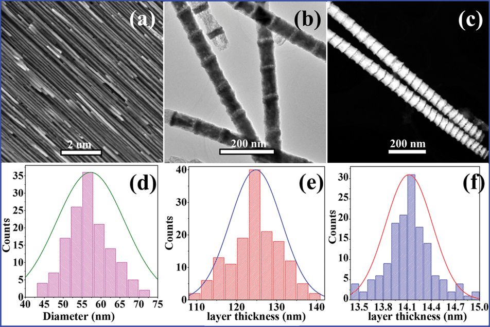 | ||
| Fig. 2 (a) SEM image of a fractured template with CoCu/Cu multilayer nanowires embedded in situ in their AAO channels. (b) Representative TEM image of multilayer nanowires, of which AAO templates have been fully dissolved. (c) HAADF-STEM image. (d) Quantitative analysis of CoCu/Cu nanowire diameter distribution. (e) Quantitative analysis of CoCu layer thickness distribution. (f) Quantitative analysis of Cu layer thickness distribution. | ||
Fig. 2b is a TEM image of the multilayer nanowires, clearly showing bamboo-like morphology with a uniform diameter and period. The black contrast layers should be the CoCu alloy (proved by chemical analysis described below) with alternating grey contrast of Cu layers with repeatable morphology, which confirms that the multilayer structure of CoCu/Cu nanowire has been successfully formed. The atomic number, Z, of Co is 27, slightly smaller than that of Cu (Z = 29).32 Due to their similar thicknesses, the contrast of Cu layers in a bright field TEM image should be a little bit blacker compared to Co or CoCu alloy layers. However, the observed contrast in Fig. 2b is converse. The intrinsic reason is believed to originate from the porous morphology of Cu layers during the preparation of electrodeposition method, which can be more clearly seen in Fig. 4b. In addition, nanowire 1 located at the top left of Fig. 2b show three brighter CoCu layers than do the other CoCu layers. Outside mechanical forces and the chemical dissolution, often peel off a part of the thick layers when the nanowires are released from the AAO templates, which causes a contrast variation during TEM observation. Moreover, individual MNWs have a uniform diameter of 55 nm (Fig. 2c), which is the same as the above SEM observations in error. The average thickness of the CoCu layers was 124 nm (Fig. 2e), and that of Cu layers was 14.2 nm (Fig. 2f) based on statistical analysis. For this specimen, the electrodeposition times were 6 s for CoCu layers and 30 s for Cu layers in a period. Then, it was calculated that the average growth rate was about 20.6 nm s−1 for Co layers and 0.5 nm s−1 for Cu layers. The CoCu growth rate was considerably faster than that of Cu, of which the main reason is believed to come from the 100 times higher concentration of CoSO4·7H2O than that of CuSO4·7H2O.
 | ||
| Fig. 3 EDX analysis of electrodeposited nanowires: (a) Co/Cu multilayer nanowires; (b) single-potential Co nanowires deposited using a potential of −1.2 V (versus SCE); (c) Cu nanowires deposited by constant potential of −0.65 V (versus SCE); (d) EDX spectra acquired from the three types of nanowires in (a)–(c), respectively. | ||
 | ||
| Fig. 4 High-resolution chemical analysis of Co/Cu multilayer nanowires: (a) EDX line scan spectra of Co Kα at 6.980 keV (red line) and Cu Kα at 7.478 keV (black line), of which scanning position is marked by red dotted line in (b); (b) HAADF-STEM image of the scanned area of the elemental mapping; (c–e) EDX elemental mappings of Co Kα, Cu Kα and their combination, respectively. | ||
The morphologies of individual CoCu/Cu multilayer nanowires were further investigated by a HAADF-STEM technique. Fig. 2c shows a representative HAADF-STEM image of the CoCu/Cu multilayer nanowires. The contrast of incoherent high-resolution HAADF-STEM images directly depends on specimen thickness (or material density) in addition to the atomic number (Z), and in the nanowire image the CoCu layers show the highest contrast when compared to the adjacent alternating Cu layers (Fig. 2d and below Fig. 4b). It can also be observed that the neighbouring nanowires have nearly the same periodicity and layer size, which is also observed in the bright-field TEM images.
The chemical analysis of the multilayer CoCu/Cu nanowires was performed using EDX and STEM mapping techniques on a 300 kV TEM. Because of the generation of secondary X-rays from adjacent layers, it is difficult to do quantitative EDX of individual layers on multilayer nanowires. In this work, we prepared additional single phase nanowires using the same AAO templates and plating electrolyte for correctly detecting the chemical composition of CoCu and Cu layers. Single phase Cu nanowires were electrodeposited by a single potential −0.65 V and single phase CoCu nanowires for −1.2 V. A single potential deposition should not significantly alter the ratio of the Co to Cu atoms compared to the pulsed deposition at the same potential.26,33 Then, the single phase nanowires were removed from the AAO templates, as were the CoCu/Cu samples, and analysed by EDX.
Fig. 3a–c shows the representative TEM images of CoCu/Cu nanowires, single-phase CoCu nanowires and Cu nanowires. Fig. 3d shows the corresponding EDX spectra measured from the CoCu/Cu, CoCu and Cu nanowires. As expected, Cu peaks are observed in all the spectra. Co peaks appear on both CoCu/Cu and CoCu nanowire spectra, revealing Co deposition at the −1.2 V applied potential (pulsed and constant). Quantitative analysis shows that the cobalt content of the CoCu single phase wires is higher compared to the multilayered CoCu/Cu wires as expected because of the presence of the Cu layers in the latter. The single phase Cu nanowire EDX spectra are consistent with the deposition of pure copper nanowires, and thus indicate pure Cu layers in the multilayered nanowires. Quantitative analysis of EDX spectra from the single phase CoCu nanowires indicates a 81![[thin space (1/6-em)]](https://www.rsc.org/images/entities/char_2009.gif) :19 atom ratio of Co:Cu, inferring a Co81Cu19/Cu composition for the multilayered nanowires deposited under our experimental conditions. In addition, the Al and O peaks on all three EDX spectra are from residue of the dissolved alumina, and the Ni and C peaks originate from carbon coated nickel grids, which were confirmed by EDX analysis of an empty carbon coated nickel grid.
:19 atom ratio of Co:Cu, inferring a Co81Cu19/Cu composition for the multilayered nanowires deposited under our experimental conditions. In addition, the Al and O peaks on all three EDX spectra are from residue of the dissolved alumina, and the Ni and C peaks originate from carbon coated nickel grids, which were confirmed by EDX analysis of an empty carbon coated nickel grid.
The chemical element distributions of Co81Cu19/Cu multilayer nanowires were further studied by HAADF-STEM, EDX line scan and EDX elemental mapping analysis techniques. Fig. 4a shows a collection of two line scan spectra taken across the multilayer nanowire using EDX Linescan, including Co Kα at 6.980 keV and Cu Kα at 8.048 keV, of which line scan position is marked by dotted red line in Fig. 4b, and the electron beam spot-size is 5 nm. Both Co Kα and Cu Kα X-ray signals oscillate along the wire as expected, with a maximum signal of Co in the CoCu layers and maximum signal of Cu in Cu layers. This result evidently reveals that our specimens are have a periodic multilayer structure. In addition, it is also observed that the Cu signal from the copper layers is a little bit lower than the Co signal from the Co81Cu19 alloy layers. The reasons are deduced to be mainly because of the resolution of the EDX detector and the atom amount of detected elements irradiated by the electron beam spot during the detection time. As observed by the above TEM and STEM morphologies, the Cu layers have a porous morphology, which causes the absolute atom amount of Cu per unit area to be larger than that of Co when the electron beam spot was scanned through their layers. Therefore, the Cu signal from copper layers itself would be weaker than the Co signal from the alloy layers. This is also the reason why the contrast of the Cu layers is darker compared to the Co81Cu19 layers under the HAADF-STEM observation, and whiter than that of the Co81Cu19 layers under TEM observation (although the Cu atomic number is larger than that of Co as mentioned above). Moreover, the resolution of our EDX detector is 20 nm, a little bit larger than the thickness of the Cu layers in this work, which indicates that the detector is not sensitive enough when the electron beam was scanned to the copper layer under the line scan model.
To further verify the distribution of two elements within the multilayer nanowires, EDX mappings of the Co and Cu elements were investigated. Fig. 4b shows the HAADF-STEM image of the single Co81Cu19/Cu multilayer nanowire, which was used for the chemical elemental distribution analysis. Fig. 4c and d display the corresponding EDX mappings of Cu (Kα at 8.048 keV) and Co (Kα at 6.980 keV) elements, respectively. The Cu elements (Fig. 4c) are observed to distribute throughout the entire nanowire, but have a very high concentration of Cu layers and a very low concentration of CoCu layers. This result indicates that copper was also generated during the electrodeposition of the Co layers, while the low concentration of Cu ions in the electrolyte and the slow growth rate led to the low content of copper in the CoCu layers. The Co element (Fig. 4d) is periodically distributed in magnetic layers, revealing a good modulation. The average thickness of the Cu modulation is approximately 14 nm, and that of CoCu is about 132 nm, which are the same as the above morphological detections by TEM and STEM. In order to well understand the distributions of two elements within a single multilayer nanowire, the mapping images of Co Kα and Cu Kα were combined as shown in Fig. 4e. The elemental mapping results confirm that individual multilayer nanowires contain an alternating CoCu and Cu layer once again, consistent with the expected CoCu/Cu structure of the multilayer nanowires. These are also in agreement with the observations of EDX line scan and morphological studies.
The crystalline structure of the Co81Cu19/Cu multilayer nanowires was characterised in detail using HRTEM, selected-area electron diffraction (SAED) and converged beam electron diffraction (CBED). Fig. 5b shows a typical SAED pattern of three Co81Cu19/Cu multilayer nanowires obtained from the area marked by a dashed circle in Fig. 5a. The rings can be well indexed to two sets of lattice planes. The green one can be well indexed to the (111), (200), (220), (311), (222), (400) and (311) planes of an fcc Cu structure with 3.61 ± 0.1 Å lattice constant, which is believed to come from the Cu layers. The red one can be well indexed to be an fcc structure of (111), (200), (220), (311), (222), (400) and (331) planes with 3.54 ± 0.1 Å lattice constant, which is believed to come from the Co81Cu19 layers. The standard JCPDS cards do not contain any phase information about bulk or other size-scaled Co81Cu19 alloy. To the best of our knowledge, there should be no report on the crystal structure of the bulk or the nanoscale Co81Cu19 alloy. Therefore, we cannot compare our measured crystal phase of Co81Cu19 layers with any previous report.
 | ||
| Fig. 5 TEM structural analysis of the Co81Cu19/Cu multilayer nanowires: (a) a bundle of nanowires; (b) SAED pattern of the area marked by a yellow dotted circle in (a); (c) a bundle of pure Co81Cu19 alloy nanowires; (d) SAED pattern of pure Co81Cu19 alloy nanowires; (e) a bundle of pure Cu alloy nanowires; (f) SAED pattern of pure Cu alloy nanowires. | ||
In order to verify the correctness of our measurement, the crystal structure of the above pure Cu nanowires and Co81Cu19 alloy nanowires were analysed for comparison in this work. Fig. 5d shows a SAED pattern of pure Co81Cu19 alloy nanowires, which is the same as the red set of lattice planes in Fig. 5b. Fig. 5f shows a SAED pattern of pure Cu nanowires, which is the same as the green set of lattice planes in Fig. 5b. This result confirms again that the crystal structure of our Co81Cu19 layers is fcc with a 3.54 ± 0.1 Å lattice constant, which should be the first reported crystal phase of a Co81Cu19 alloy.
The crystal structures of the inside Co81Cu19 layers, inside Cu layers and the interfaces between them were also examined. Fig. 6a shows a representative HRTEM image of a Co81Cu19/Cu period, displaying two clear interfaces of Co81Cu19/Cu and Cu/Co81Cu19 marked by yellow dotted lines. However, both the interfaces show a zig-zag shape, indicating a rough edge. The thickness of the non-magnetic Cu layer is measured to be approximately 12 nm, and that of the interfaces (transition region between the Co81Cu19 and Cu layer) is around 2 nm. The lattice-resolution HRTEM image and CBED analysis reveal that both Cu layers and Co81Cu19 layers are polycrystalline with an fcc structure. The diameter of most crystallites is measured in the range of 5–15 nm. As examples, Fig. 6c shows a lattice-level HRTEM image of a ∼13 nm Co81Cu19 single crystal, of which the top-left inset is its corresponding CBED pattern. The interplanar distances are measured to be 2.04 ± 0.1 Å and 1.77 ± 0.1 Å, matching with (111) and (200) planes of fcc Co81Cu19 with [011] orientation. The representative lattice-level HRTEM image of a Cu single crystal inside a Cu layer is shown in Fig. 6d, of which the relevant CBED pattern is shown in its top-left inset. The interplanar distances are measured to be 2.05 ± 0.1 Å and 1.81 ± 0.1 Å, well matched with the (111) and (200) planes of fcc Cu with [011] orientation.
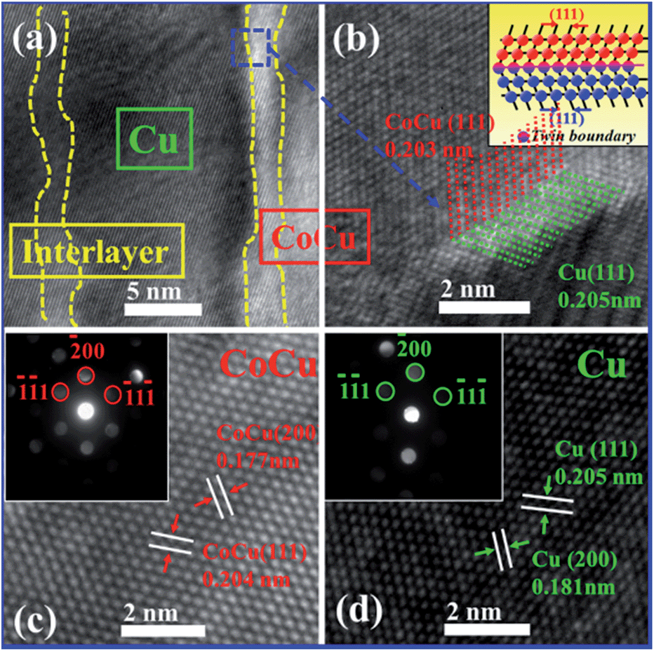 | ||
| Fig. 6 TEM structural analysis of the Co81Cu19/Cu multilayer nanowires: (a) a period of Co81Cu19/Cu nanowires; (b) atomic-level HRTEM image of the area marked by blue square A in (a). Inset, the schematic geometry of stacking faults with fcc structure. (c) atomic-level HRTEM image of Co81Cu19 layer. Inset, its corresponding CEBD pattern; (d) atomic-level HRTEM image of Cu layer. Inset, its corresponding CEBD pattern. | ||
Fig. 6b shows a lattice resolution TEM image of the interface between neighbouring Cu and Co81Cu19 grains in Fig. 6a (marked by the blue square). It is clearly seen that Cu {111} planes and Co81Cu19 {111} planes stack on each other and form a twin structure. This result directly confirms the theoretical prediction that an error rotating fcc crystal by 180° about <111> creates a twin because the {111} planes of fcc structure are not the planes of the space group.34 As detected by the above SAED, the lattice constants of Cu and Co81Cu19 are 3.61 Å and 3.55 Å, respectively. Their lattice mismatch ratio (Δa/a) (in our case, (aCu − aCo81Cu19)/aCo81Cu19) is calculated to be about 1.97%, providing an ideal condition occurring one perfect edge dislocation. The dislocation eventually releases the compression from Cu crystalline, which is deduced to be the intrinsic reason of forming the twin structure during the growth of the multilayer nanowire.35 The top-right inset in Fig. 6b shows a schematic geometry of stacking faults, which reveals the formation of a twin structure in fcc structures as in our observation here. It is known that the resistance of the FM/NM multilayer structure is relatively high when the neighbouring FM layers are in an anti-parallel alignment, and their resistance is relatively low when the FM layers are parallel alignment. However, twin structures may destroy the phase coherence of conduction electrons, which is a disadvantage for the GMR effect.37,38 Therefore, it is believed that this observation also reveals the intrinsic reason why the GMR effect of the specimens prepared by the electrodeposition method is universally smaller than those prepared by a high-vacuum sputtering method or a molecular beam epitaxy (MBE) method.26,27
The magnetic properties of the Co81Cu19/Cu multilayer nanowires were measured by a VSM with the applied field at different angles (θ) between the external field and nanowire length axis. Fig. 7a shows two hysteresis curves of the Co81Cu19/Cu multilayer nanowire arrays measured at room temperature with an applied field up to 1.6 T at 0° and 90° angles. The coercivity and squareness are 1098 Oe and 0.46, respectively when the applied field is parallel to the length axis of the multilayer nanowires (0°, blue curve marked by hollow dots in Fig. 7a), whilst 254 Oe and 0.04, respectively for the perpendicular position (90° red curve in Fig. 7a). Fig. 7b and c show the angular dependences of the squareness and coercivity (HC(θ)), respectively. The squareness is tuned between 0.46 and 0.04 by adjusting θ, and the coercivity ranges from 1098 Oe to 254 Oe. The bell-type squareness curve (Fig. 7b) shows that the squareness reaches a maximum value when the external field is parallel to the length axis of the multilayer nanowires, and reaches minimum value when the external field is perpendicular to the length axis of the multilayer nanowires. This result reveals that the easy axis of individual Co81Cu19/Cu multilayer nanowires is aligned along the nanowire length axis.
 | ||
| Fig. 7 (a) Representative hysteresis loops of the Co81Cu19/Cu nanowires arrays measured at room temperature, of which the blue curve is recorded when the applied field is parallel to the length axis of nanowires, and the red curve for perpendicular field; (b) the bell-typed angular dependence of squareness Mr/Ms; (c) M-typed angular dependences of coercivity; (d) Illustration of the magnetisation curling and coherent rotation reversal mechanism in a single CoCu/Cu nanowire. | ||
Angular dependence of coercivity also provides the information on the magnetisation reversal mechanism. Typically, a bell-shaped HC(θ) curve for magnetic nanowires based on an infinite cylinder model indicates a coherent rotation mode of magnetisation reversal mechanism, and other-bell-shaped curves are for a curling mode. In our case, the M-type HC(θ) curve as shown in Fig. 7c cannot be simply fitted by either a bell-shape or other-bell-shape, which indicates complicated magnetic reversal mechanisms may occur in our Co81Cu19/Cu multilayer nanowire when θ was tuned. According to other reports,36 the curve as shown in Fig. 7c should indicate a transition from a curling mode rotation to a coherent mode rotation.
In order to understand the magnetization reversal mechanism of our individual Co81Cu19/Cu multilayer nanowire under the tuned magnetised field, micro-magnetic simulations using public OOMMF software has been employed.39,40 The geometrical structure and magnetic parameters used in the simulation were based on our above morphological observations and magnetic measurements. As determined by above TEM observations, the length of our multilayer nanowire is about 30 μm. In order to make the amount of calculations handleable for our computing server, the structure only composed of three periods of CoCu/Cu multilayer nanowire with 56 nm diameter was simulated. Considering that the magnetic interaction between the first magnetic layer and the fourth magnetic layer is very weak and ignorable, it is believed that this structure with three periods could reveal the intrinsic magnetic reversal mechanism of our prepared 30 μm Co81Cu19/Cu multilayer nanowire. The thickness of the CoCu layer was set to 125 nm, and that of Cu layer to 15 nm based on the experimental measurement above. The cell size was divided into 2 × 2 × 5 nm3, and the saturated magnetisation (Ms) and exchange constant (A) for CoCu layer (herein, Ms and A of bulk Co are used to replace that of CoCu because there is no report on these parameters for the Co81Cu19 alloy, and the Cu composition is low in our Co81Cu19 layers) were 1.4 × 10⁶ A m−1 and 1.3 × 10⁻¹¹ J m−1, respectively.41 As copper is a non-magnetic material, both Ms and A were set to 0, which is the same as others' treatment.40–42Fig. 8a–g show a simulated process of the magnetisation reversal of CoCu/Co multilayer nanowires when the angle between external field and multilayer nanowire length axis was 0°. A large external magnetic field along the length axis of a multilayer nanowire was first applied to completely saturate its magnetisation, and then the external field was gradually reduced in the opposite direction. It was observed that the magnetic moments reverse from the two ends of each magnetic CoCu layer, and then nearly all moments start to reverse. During this process, both the ends of each magnetic layer form spirals. If observed along with the nanowire cross-section, the distribution of magnetic moments displays vorticity as shown in Fig. 8o. The spirals propagate to the centre of each magnetic layer and eventually lead to the inversion of magnetic moments, which is consistent with the curling mode.
 | ||
| Fig. 8 Magnetisation reversal simulations of individual Co81Cu19/Cu multilayer nanowires with 56 nm diameter and an FM (125 nm)/NM (10 nm)/FM (125 nm)/NM (10 nm)/FM (125 nm) structure: (a)–(g), distributions of magnetic moments along nanowire length axis at different reversal time when the external field was applied to be parallel to nanowire length axis (θ = 0°); (h)–(n), distributions of magnetic moments along nanowire length axis at different reversal time at = 90°; (o)–(x), cross sectional distributions of magnetic moments at 0°, 10°, 20°, 30°, 40°, 50°, 60°, 70°, 80°, and 90° when the opposite field was just applied; (y) the relevant angular dependence of simulated squareness Mr/Ms; (z) the relevant angular dependences of simulated coercivity. | ||
Fig. 8h–n show the simulated magnetisation reversal process occurring when the external field is perpendicular to the multilayer nanowire length axis (90°). Similar to the above parallel situation (0°), a large external magnetic field perpendicular to the length axis of multilayer nanowire was first applied to make its magnetization completely saturated, and then the external field gradually reduced in the opposite direction. It is seen that nuclei of reversed domains were formed at the two ends of each magnetic layers when the opposite field is initially applied (Fig. 8i), and then they propagate until all magnetic moments were reversed (Fig. 8j–n). The cross-sectional distribution of magnetic moments in the initial moments when the opposite field was applied is shown in Fig. 8x. This result clearly reveals a coherent rotation mechanism occurring on individual Co81Cu19/Cu multilayer nanowires after a perpendicular external field was applied to the multilayer nanowire length axis.
The magnetic reversal processes of the Co81Cu19/Cu multilayer nanowire under other angles ranging from 0° to 90° have also been simulated. Fig. 8p–w show the relevant cross-sectional distributions of magnetic moments at 10°, 20°, 30°, 40°, 50°, 60°, 70° and 80° between the external field and multilayer nanowire length axis when the opposite field was just applied. Combining the 0° and 90° situations, it is seen that the nuclei of reversed domain appear in a different distribution of magnetic moments. At 0° (Fig. 8o), the magnetic moments form an ideal vortex, of which the centre is located in the middle of the nanowire cross-section. As the external field angle increases (Fig. 8o–x), the centre of the vortex diverges from the centre of the nanowire cross-section. When the external field angle θ is 90°, the magnetic moments become a distribution of coherent rotation. These simulations prove that there is a transition from the curling mode to coherent rotation in the magnetisation reversal mechanism of the Co81Cu19/Cu multilayer nanowire as the angle between the external field and multilayer nanowire length axis increases. This result is consistent with above experimental measurement of H(θ) as shown in Fig. 7c.
Fig. 8y and z show the simulated relationship of squareness and coercivity and the external field angle θ. It is seen that both of them show the same trends as the experimental data of Fig. 7b and c, which reveals a consistence of our simulations with the experiments. However, the simulated coercivities at all angles are smaller than their relevant experimental values. The intrinsic reason is deduced to come from the pinning effect coercivity in CoCu layers in reality, while it was not considered in our theoretic simulation. Meanwhile, the simulated data in Fig. 8z has a pronounced dip in comparison with the experimental data in Fig. 7c. The reason is believed to originate from the magneto-static interaction among the neighbouring nanowires, which was also not considered in our theoretic simulation.45 In addition, it is notable that the magnetic reversal processes of all magnetic layers are exactly the same and synchronous when the external field is either parallel or perpendicular to the nanowire length axis. The intrinsic reason is believed to originate from the separation of the 15 nm non-magnetic Cu layer, causing an ignorable dipole-dipole interaction between neighbouring magnetic layers. This result also confirms that the simplified multilayer structure used in this simulation can represent the intrinsic magnetic reversal mechanism of our real 30 μm Co81Cu19/Cu multilayer nanowires.
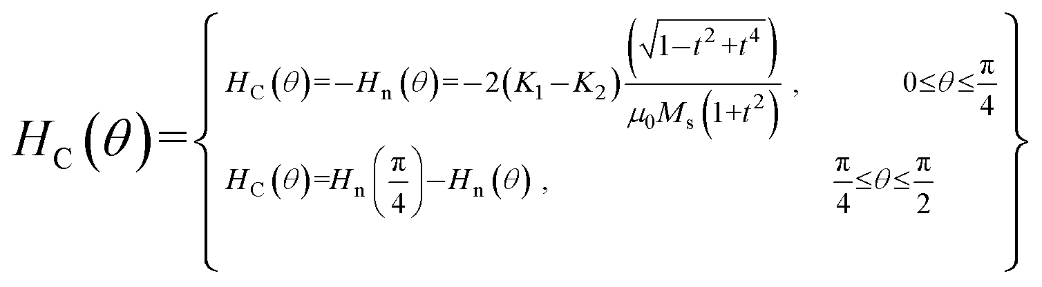
In order to further confirm the correctness of our above simulations, the coercivities of the multilayer wire structure at 0° and 90° field angles were theoretically calculated. According to the reported theoretical analysis of micromagnetism,39,42 the coercivity for a curling mode is governed by eqn (1):
 | (1) |
 | (2) |
The coercercity governed by coherent rotation mode can be obtained by eqn (3):43,44
 | (3) |
4 Conclusions
In conclusion, we have demonstrated a detailed high spatial resolution investigation of the morphological, chemical, structural and magnetic properties of Co81Cu19/Cu multilayer nanowires fabricated by a dc electrodeposition technique into AAO templates. It was determined that individual nanowires have a regular periodic structure with a smooth surface. The Co81Cu19 and Cu layers are polycrystalline with an fcc lattice structure, and a twin structure via Co81Cu19 layer {111} planes stacking on Cu layer {111} planes was observed. The interlayer between Co81Cu19 and Cu layers is about 2 nm. Co layers are proved to present about 19% Cu by EDX analysis due to a co-electrodeposition. The magnetic properties show that the Co81Cu19/Cu nanowires arrays have an easy axis parallel to the length axis of the wires. Furthermore, the experimental measurements and theoretic simulations prove that there is a transition from the curling mode to coherent rotation in the magnetisation reversal mechanisms of individual Co81Cu19/Cu multilayer nanowires with increasing angle between external field and multilayer nanowire length axis ranging from parallel position to perpendicular position.Acknowledgements
This work was supported by National Basic Research Program of China (2012CB933104), National Natural Science Foundation of China (11274145 and 11034004), MOST International Cooperation Funds (2014DFA91340), Program for Changjiang Scholars and Innovative Research Team in University (Grant no. IRT1251), the Fundamental Research Funds for the Central Universities (lzujbky-2013-19, and 2022013zrct01).Notes and references
- Y. Jyoko, S. Kashiwabara and Y. Hayashi, J. Electrochem. Soc., 1997, 144, L5–L8 CrossRef CAS PubMed.
- E. Comini, C. Baratto, G. Faglia, M. Ferroni, A. Vomiero and G. Sberveglieri, Prog. Mater. Sci., 2009, 54, 1–67 CrossRef CAS PubMed.
- D. Li, R. S. Thompson, G. Bergmann and J. G. Lu, Adv. Mater., 2008, 20, 4575–4578 CrossRef CAS.
- A. Fert and L. Piraux, J. Magn. Magn. Mater., 1999, 200, 338–358 CrossRef CAS.
- S. Parkin, X. Jiang, C. Kaiser, A. Panchula, K. Roche and M. Samant, Proc. IEEE, 2003, 91, 661–680 CrossRef CAS.
- Y. Cui, Q. Q. Wei, H. K. Park and C. M. Lieber, Science, 2001, 293, 1289–1292 CrossRef CAS PubMed.
- M. N. Baibich, J. M. Broto, A. Fert, D. F. Van and F. Petroff, Phys. Rev. Lett., 1988, 61, 2472–2475 CrossRef CAS.
- S. Parkin, N. More and K. P. Roche, Phys. Rev. Lett., 1990, 64, 2304–2307 CrossRef CAS.
- D. Zhang, Z. Liu, S. Han, C. Li, B. Lei and M. P. Stewart, Nano Lett., 2004, 11, 2151–2155 CrossRef.
- M. Tanase, D. M. Silevitch, A. Hultgren, L. A. Bauer, P. C. Searson and G. J. Meyer, J. Appl. Phys., 2002, 91, 8549–8851 CrossRef CAS PubMed.
- D. Kelly, J.-E. Wegrowe, T.-K. Truong, X. Hoffer and J.-P. Ansermet, Phys. Rev. B: Condens. Matter Mater. Phys., 2003, 68, 134425 CrossRef.
- P. N. Loxley, J. Magn. Magn. Mater., 2002, 249, 187–192 CrossRef CAS.
- S. Valizadeh, J. M. George, P. Leisner and L. Hultman, Thin Solid Films, 2002, 402, 262–271 CrossRef CAS.
- L. Piraux, S. Dubois, J. L. Duvaip, K. Ounadjela and A. Fert, J. Magn. Magn. Mater., 1997, 175, 127–136 CrossRef CAS.
- J. U. Cho, J. H. Wu, J. H. Min, J. H. Lee, H. L. Liu and Y. K. Kim, J. Magn. Magn. Mater., 2007, 310, 2420–2422 CrossRef CAS PubMed.
- J. U. Cho, J. H. Min, S. P. Ko, J. Y. Soh, Y. K. Kim, J.-H. Wu and S. H. Choi, J. Appl. Phys., 2006, 99, 08C909 CrossRef PubMed.
- M. Shima, L. Salamanca-Riba, T. P. Moffat and R. D. McMichael, J. Magn. Magn. Mater., 1999, 198–199, 52–54 CrossRef CAS.
- T. Ohgai, X. Hoffer, L. Gravier and J.-Ph. Ansermet, J. Appl. Electrochem., 2004, 34, 1007–1012 CrossRef CAS.
- P. Shakya, B. Cox and D. Davis, J. Magn. Magn. Mater., 2012, 324, 453–459 CrossRef CAS PubMed.
- H. P. Liang, Y. G. Guo, J. S. Hu, C. F. Zhu, L. J. Wan and C. L. Bai, Inorg. Chem., 2005, 44, 3013–3015 CrossRef CAS PubMed.
- X.-T. Tang, G.-C. Wang and M. Shima, IEEE Trans. Magn., 2006, 42, 2975–2977 CrossRef CAS.
- N. Rajasekaran, L. Pogány, Á. Révész, B. G. Tóth, S. Mohan, L. Péter and I. Bakonyi, J. Electrochem. Soc., 2014, 161, D339–D348 CrossRef CAS PubMed; D. Rafaja, C. Schimpf, T. Schucknecht, V. Klemm, L. Péter and I. Bakonyi, Acta Mater., 2011, 59, 2992–3001 CrossRef PubMed.
- L. Wang, K. Y. Zhang, A. Metrot, P. Bonhomme and M. Troyon, Thin Solid Films, 1996, 288, 86–89 CrossRef CAS.
- Y. Peng, T. Cullis, G. Möbus, X. Xu and B. Inkson, Nanotechnology, 2007, 18, 485704 CrossRef.
- M. Jamali, K. Narayanapillai, X. P. Qiu and L. M. Loong, Phys. Rev. Lett., 2013, 111, 246602 CrossRef.
- M. Hecker, J. Thomas, D. Tietjen, S. Baunack, C. M. Schneider, A. Qiu, N. Cramer, R. E. Camley and Z. Celinski, J. Phys. D: Appl. Phys., 2003, 36, 564–572 CrossRef CAS; X. T. Tang and G. C. Wang, J. Appl. Phys., 2006, 99, 033906 CrossRef PubMed.
- J. C. A. Huang, Y. H. Lee, Y. M. Hu and T. C. Chang, J. Appl. Phys., 1996, 79, 6276–6278 CrossRef CAS PubMed; K. Tsutsumi, P. De Haan, M. Eisenberg, D. Monsma and J. C. Lodder, J. Magn. Magn. Mater., 1996, 156, 327–328 CrossRef.
- K. Qi, X. H. Li, H. Zhang, L. Wang, D. S. Xue, H. L. Zhang, B. F. Zhou, N. J. Mellors and Y. Peng, Nanotechnology, 2012, 23, 505707 CrossRef PubMed.
- K. Y. Kok, C. M. Hangarter, B. Goldsmith, I. K. Ng, N. B. Saidin and N. V. Myung, J. Magn. Magn. Mater., 2010, 322, 3876–3881 CrossRef CAS PubMed.
- Y. Peng, T. Cullis, G. MÖbus, X. J. Xu and B. Inkson, Nanotechnology, 2009, 20, 395708 CrossRef PubMed.
- Y. Peng, T. Cullis and B. Inkson, Nano Lett., 2009, 9, 91–96 CrossRef CAS PubMed.
- G. Martínez, N. M. Baibich, M. G. Miranda and E. Vargas, J. Magn. Magn. Mater., 2004, 272–276, 1716–1717 CrossRef PubMed.
- S. B. Valizadeh, L. Hulman, J. M. George and P. Leisner, Adv. Funct. Mater., 2002, 12, 766–772 CrossRef CAS.
- J. L. Maurice, D. Imhoff, P. Etienne, D. Durand, S. Dubois, L. Piraux, J. M. George, P. Galtier and A. Fert, J. Magn. Magn. Mater., 1998, 184, 1–18 CrossRef CAS.
- M. Yuasa, H. Nakano and M. Mabuchi, J. Phys.: Conf. Ser., 2013, 417, 012064 CrossRef.
- W. Wernsdorfer, B. Doudin, D. Mailly, K. Hasselbach, A. Benoit and J. Meier, Phys. Rev. Lett., 1996, 77, 1873–1876 CrossRef CAS.
- P. L. Rossiter, The Electrical Resistivity of Metals and Alloys Cambridge, University Press, New York, 1987 Search PubMed.
- D. W. Callister Jr, Materials Science and Engineering, An Introduction, Wiley, New York, 2000 Search PubMed.
- M. Donahue and D. Porter, http://math.nist.gov/oommf.
- G. Mohlera and A. W. Harter, J. Appl. Phys., 2005, 97, 10E313 Search PubMed.
- Y. Zhou, J. Åkerman and J. Z. Sun, Appl. Phys. Lett., 2011, 98, 102501 CrossRef PubMed.
- A. Aharoni and S. Shtrikman, Phys. Rev., 1958, 109, 1522–1528 CrossRef.
- G. C. Han, B. Y. Zong, P. Luo and Y. H. Wu, J. Appl. Phys., 2003, 93, 9202 CrossRef CAS PubMed.
- L. G. Vivas, M. Vazquez, J. Escrig, S. Allende, D. Altbir and D. C. Leitao, Phys. Rev. B: Condens. Matter Mater. Phys., 2012, 85, 035439 CrossRef.
- D. Kaur, S. Chaudhary, D. K. Pandya, R. Gupta and R. K. Kotnala, J. Magn. Magn. Mater., 2013, 344, 72–78 CrossRef CAS PubMed.
Footnote |
| † Electronic supplementary information (ESI) available. See DOI: 10.1039/c4tc01510j |
| This journal is © The Royal Society of Chemistry 2015 |