
Nondoped deep-blue spirofluorenexanthene-based green organic semiconductors (GOS) via a pot, atom and step economic (PASE) route combining direct arylation with tandem reaction†
Ming-Li
Sun
a,
Wen-Sai
Zhu
c,
Zhen-Song
Zhang
b,
Chang-Jin
Ou
a,
Ling-Hai
Xie
*a,
Yang
Yang
c,
Yan
Qian
a,
Yi
Zhao
b and
Wei
Huang
*ac
aCenter for Molecular Systems and Organic Devices (CMSOD), Key Laboratory for Organic Electronics & Information Displays (KLOEID), Institute of Advanced Materials (IAM), Nanjing University of Posts & Telecommunications, Nanjing 210046, Jiangsu, China. E-mail: wei-huang@njtech.edu.cn; iamlhxie@njupt.edu.cn; Fax: +86 25 5813 9988; Tel: +86 25 5813 9001
bState Key Laboratory of Integrated Optoelectronics, College of Electronics Science and Engineering, Jilin University, Changchun 130012, Jilin, China
cJiangsu-Singapore Joint Research Center for Organic/Bio-Electronics & Information Displays, Institute of Advanced Materials (IAM), Nanjing Tech University, Nanjing 211816, Jiangsu, China
First published on 23rd October 2014
Abstract
Effective synthesis of organic semiconductors with pot, atom, and step economic (PASE) methods will be an indispensable part of green electronics. In this paper, we combined direct arylation with one-pot/tandem reaction to synthesize a green organic semiconductor (GOS), di(spiro[fluorene-9,9′-xanthene]-2-yl)-1,2,4,5-tetrafluorobenzene (DSFX-TFB), serving as the emitting layer for organic light-emitting devices (OLEDs). The maximum current efficiency (CE) of 3.2 cd A−1, power efficiency (PE) of 2.0 lm W−1 and external quantum efficiency (EQE) of 4.1% were obtained with the CIE coordinates (0.15, 0.08) in the nondoped deep-blue OLEDs. Meanwhile, good energy transfer and device performances with maximum CE of 8.03 cd A−1 and PE of 4.62 lm W−1 were achieved in typical sky-blue fluorescent OLEDs using DSFX-TFB as host and p-bis(p-N,N-diphenyl-aminostyryl)benzene (DSA-Ph) as dopant material. This work provides a PASE synthetic route for GOSs and eco-friendly materials.
1. Introduction
Green electronics is a necessary part of sustainable economic and social development. In recent years, viable organic electronics are on the rise due to advantages such as low cost, large-area processing and even wearable textile compared to inorganic counterparts.1 Exploration of green organic semiconductors (GOS) in wearable electronics is also underway. Ideal GOSs should have four fundamental features: (1) biomass or renewable feedstocks rather than fossil raw materials;2–4 (2) atom economic synthetic route with less hazardous reagents;5,6 (3) low energy consumption and eco-friendly aqueous film-forming process;7 (4) finally obtained organic devices with low toxicity and biodegradability.8 Until now, there are no organic semiconductors that meet all above mentioned four features. Based on the second feature, it is one crucial challenge to design effective synthetic routes to GOSs with the pot, atom, and step economic (PASE) procedure developed by Clarke and co-workers for the synthesis of tetrahydropyran-4-ones.9 In general, organic semiconductors were synthesized by traditional transition metal-catalyzed cross-coupling reactions, such as the Suzuki and/or Stille reaction, which usually require a precursor with boronic acid groups and/or toxic tin groups.5,10 Recently, C–H bond activation11,12 has become an alternative synthetic technology with an atom economic and greener character for the design of organic semiconductors.13–16 In addition, more concise and pot-economic synthesis methods, such as tandem reaction,17,18 domino reaction,19,20 and multicomponent reaction21–23 have been explored to synthesize building blocks for sustainable organic semiconductors. However, it is rare to make synthetic schemes of organic semiconductors by combining various green and sustainable methods.It is a powerful synthetic tool to combine direct arylation with tandem reaction to synthesize GOSs since most organic pi-semiconductors belong to arenes. In our previous work, we discovered a concise one-pot method for synthesizing spiro-building blocks such as spirofluorenexanthene (SFX),18 and created a series of SFX-based, organic light-emitting materials24–27 that have been confirmed to have excellent device performances equivalent to spirobifluorene counterparts. In this work, we first combined direct arylation with one-pot/tandem reaction with PASE to synthesize a dumbbell-shaped fluorescent organic semiconductor, di(spiro[fluorene-9,9′-xanthene]-2-yl)-1,2,4,5-tetrafluorobenzene (DSFX-TFB), for high-efficiency nondoped deep-blue-emitting OLEDs. In our design, tetrafluorobenzene was introduced into DSFX-TFB primarily based on the following considerations. (1) The tetrafluorobenzene group as an electron-withdrawing moiety benefits electron injection that can balance carrier transport in the design of bipolar organic semiconductors. Meanwhile, it can also make spectrum blue shift and improve colour purity.28–30 (2) Electron-deficient tetrafluorobenzene facilitates the activation of C–H bonds that make direct arylation reaction with brominated SFX easy to accomplish.31–33 It has already been incorporated into polymers and other small molecules via direct arylation.13,14,31,33–35 (3) SFX-capped tetrafluorobenzene forms a dumbbell-shaped molecule that is favorable for the suppression of intermolecular packing,25 which can be expected to produce high device performance and better material stability.36–38 As a result, we used only a two-step concise and effective reaction to synthesize the DSFX-TFB and fabricated a preliminary device with a configuration of ITO/MoOx (2 nm)/m-MTDATA (20 nm)/NPB (10 nm)/DSFX-TFB (30 nm)/Bphen (40 nm)/LiF (1 nm)/Al. The device exhibited good current efficiency (CE, 3.2 cd A−1), power efficiency (PE, 2.0 lm W−1), external quantum efficiency (EQE, 4.1%), and deep-blue emission with enhanced colour purity of CIE coordinates (0.15, 0.08). In addition, the maximum CE of 8.03 cd A−1 and PE of 4.62 lm W−1 were obtained in the typical host–guest OLEDs using DSFX-TFB![[thin space (1/6-em)]](https://www.rsc.org/images/entities/char_2009.gif) :DSA-Ph (3 wt%) as the emitting layer.
:DSA-Ph (3 wt%) as the emitting layer.
2. Results and discussion
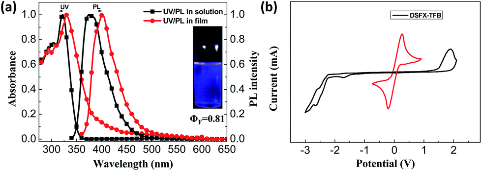
The synthetic route of DSFX-TFB as green advanced material is outlined in Scheme 1. As in our previous work,18 2-BrSFX was synthesized via a tandem protocol of 2-bromofluorenone with overdose phenol under methylsulfonic acid at 150 °C. This greener synthesis need not be separated by column chromatography with more than 75% yield. The target DSFX-TFB was obtained through direct arylation of 2-BrSFX with 1,2,4,5-tetrafluorobenzene using Pd(OAc)2 as the catalyst with a yield of 70%. The product was confirmed by 1H-NMR spectroscopy and MALDI-TOF mass spectroscopy (Fig. S1†) and found to be in good agreement with the structure. DSFX-TFB showed high decomposition temperature (440 °C) and no obvious glass-transition temperatures (Tg) (Fig. S2†). The absorption spectrum of DSFX-TFB showed a main absorption band at 322 nm in dilute chloroform solution and at 330 nm in thin film corresponding to the π → π* transition of the π-conjugated cores (Fig. 1a). The photoluminescence (PL) emission peak of DSFX-TFB was observed at 375 nm in chloroform solution and 401 nm in thin film with a red shift of 26 nm (Fig. 1a), respectively. Nevertheless, the PL spectrum in thin film exhibited the same narrow full widths at half maximum (FWHM) of 54 nm as that in solution (Table S1†). And due to the introduction of fluorine atoms, the PL spectrum obviously shifted blue compared with 1,4-di(spiro[fluorene-9,9′-xanthen]-2-yl)benzene (DSFXB) (for synthesis and characterization, see Fig. S3†), which exhibited the maximum emission peak at 417 nm in film (Fig. S4†). The fluorescence quantum efficiency of DSFX-TFB in solution is 0.81 and the value also can be as high as 0.66 in film. Such efficient solid-state deep-blue emission should be partially attributed to the dumbbell-shaped conformation that effectively suppresses molecular packing. Cyclic voltametry (CV) (Fig. 1b) was measured to estimate its HOMO (−6.1 eV), LUMO (−2.4 eV), and bandgap (3.7 eV). The low LUMO is consistent with other fluorinated polymers and small molecules that have been widely developed and used in organic semiconductors,29,30 suggesting that the electron-injection ability of DSFX-TFB was improved due to introduction of fluorine atoms as compared with DSFXB whose LUMO is −2.27 eV (Fig. S5†).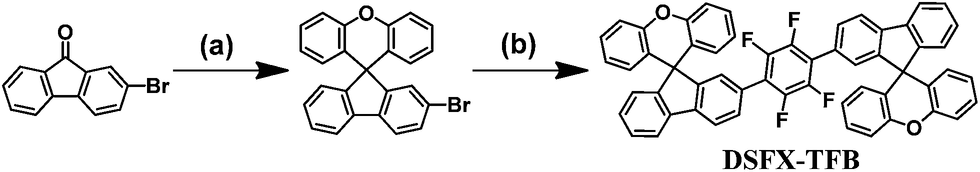 | ||
| Scheme 1 Synthetic procedures for the DSFX-TFB. Reaction conditions: (a) phenol, MeSO3H, 150 °C, 8 h, 75%. (b) 1,2,4,5-tetrafluorobenzene, Pd(OAc)2, PtBu2Me–HBF4, K2CO3, DMAc, 150 °C, reflux 36 h, 70%. | ||
 | ||
| Fig. 1 UV-Vis and PL spectra in dilute chloroform and in thin film (a) and cyclic voltammograms of reduction in THF solution and oxidation in CH2Cl2 solution (b) for DSFX-TFB. | ||
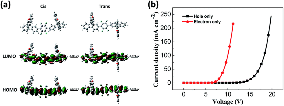
According to DFT calculations, DSFX-TFB exhibits cis and trans conformations that have the same stability due to very close frontier orbital energy levels (Fig. 2a). This probably results in a less obvious shoulder peak at about 386 nm in the emission spectrum of the DSFX-TFB film, which makes the entire spectrum look slightly wider (Fig. 1a). All the HOMOs and LUMOs are mainly concentrated at the π-conjugated backbone comprised of the benzene ring and fluorene units in either conformation. The charge is not localized in a specific location even in the presence of fluorine atoms, which ensures good charge transport properties of DSFX-TFB.
 | ||
| Fig. 2 HOMO and LUMO calculated using the B3LYP/6-31G basis set (a) and current density versus voltage characteristics of the hole-only and electron-only devices (b) for DSFX-TFB. | ||
The hole-only device with the structure of glass/ITO/MoOx (2 nm)/NPB (30 nm)/DSFX-TFB (30 nm)/NPB (30 nm)/MoOx (2 nm)/Al (100 nm) and electron-only device with the structure of glass/Al (80 nm)/Cs2CO3 (1 nm)/Bphen (40 nm)/DSFX-TFB (40 nm)/Bphen (40 nm)/Cs2CO3 (1 nm)/Al (100 nm) were fabricated to investigate the charge-transport of DSFX-TFB. The current density–voltage characteristics of these single-carrier devices are shown in Fig. 2b. It can be determined that DSFX-TFB has the property of hole- and electron-transport that facilitates the charge carrier balance. But the electron current density is higher than the hole current density, indicating that DSFX-TFB exhibits better electron-transport ability than hole-transport capacity.
To investigate the potential nondoped device applications of DSFX-TFB, a series of devices, A–E, were fabricated with multilayer configurations (Fig. 3). First, we fabricated devices A–C, which have the same configuration of ITO/MoOx (2 nm)/NPB (30 nm)/DSFX-TFB (30 nm)/electron-transporting layer (ETL) (40 nm)/LiF (1 nm)/Al. All the devices have the same total thickness of organic films (100 nm). In devices A–C, DSFX-TFB served as blue light emitter, a thin-layer MoOx (2 nm) and LiF (1 nm) acted as anode and cathode buffer layer, and NPB as the hole-injecting and transporting layer. Bphen, TPBi and Alq3 were used in the ETL to transport electrons and block hole/exciton. The molecular structures of these organic compounds are shown in Fig. 3. The current density–voltage–luminance (J–V–L) characteristics, efficiencies versus luminance and normalized EL spectra of devices A–C are compared in Fig. 4. The EL performances of devices A–C are summarized in Table 1.
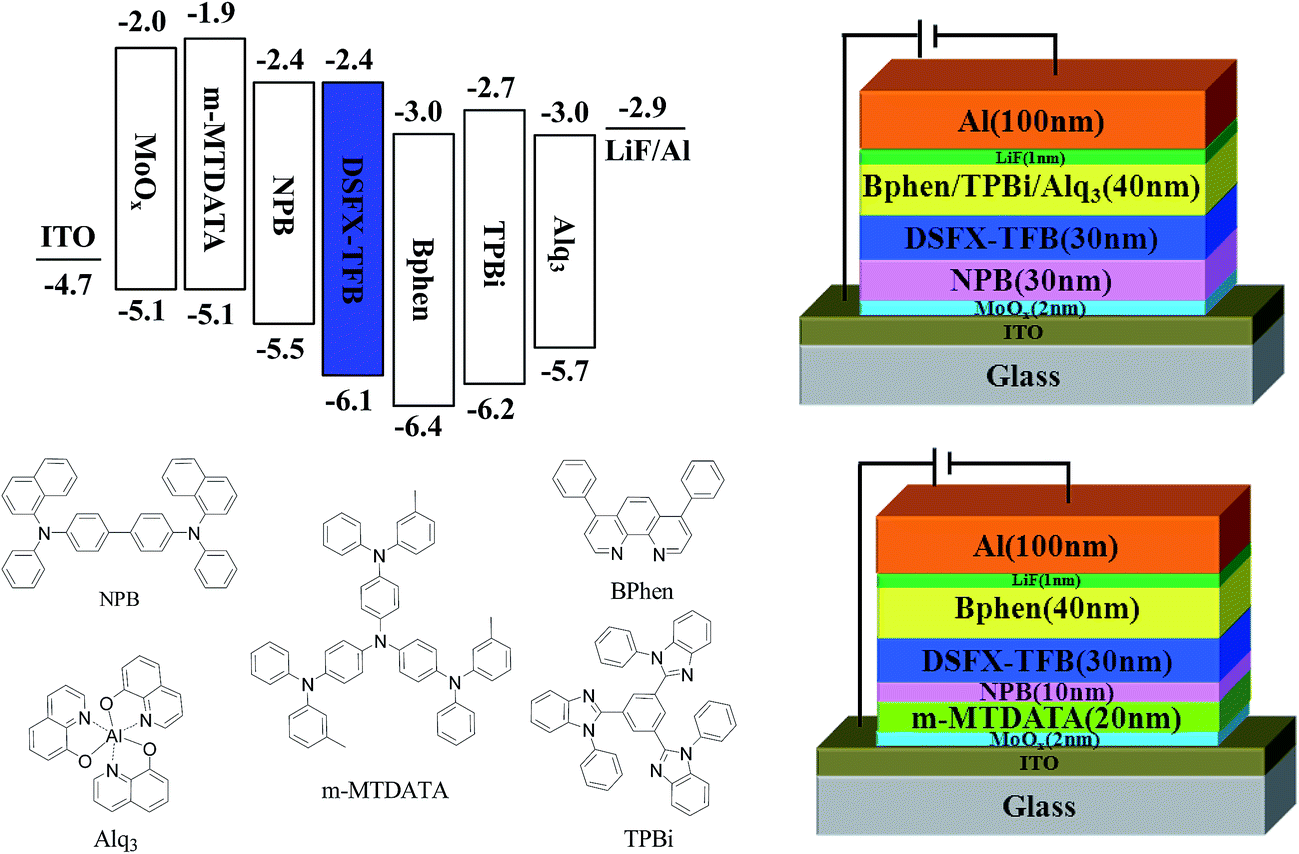 | ||
| Fig. 3 Structure diagram of devices A–E and chemical structures of used materials. | ||
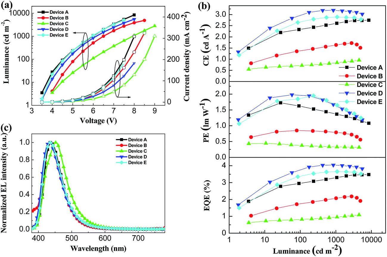 | ||
| Fig. 4 (a) J–V–L characteristics of devices A–E. (b) Efficiency characteristics of devices A–E. (c) Normalized EL spectra of devices A–E at 6 V. | ||
| Device | V on (V) | Emission peaksb/FWHM (nm) | CIEx,yb | EQEc (%) | Current efficiency | Power efficiencyc (lm W−1) |
|---|---|---|---|---|---|---|
| a Defined as onset voltage of log(J)–V curve. b At brightness of 4000 cd m−2. c Maximum values and values at 4000 cd m−2. | ||||||
| A | 3.45 | 439/62 | (0.15, 0.08) | 3.5/3.4 | 2.7/2.7 | 1.7/1.2 |
| B | 3.91 | 436/63 | (0.15, 0.07) | 2.2/2.1 | 1.7/1.6 | 0.8/0.6 |
| C | 3.82 | 453/74 | (0.16, 0.10) | 1.1/1.1 | 1.0/0.9 | 0.5/0.3 |
| D | 3.47 | 433/65 | (0.15, 0.08) | 4.1/3.9 | 3.2/3.1 | 2.0/1.3 |
| E | 3.48 | 436/65 | (0.15, 0.07) | 3.7/3.6 | 2.9/2.8 | 1.9/1.3 |
Device A exhibited the lowest turn-on voltage of 3.45 V among the three devices and the best performance, as in maximum CE of 2.7 cd A−1, PE of 1.7 lm W−1 and EQE of 3.5% (Fig. 4b and Table 1). And it obtained deep-blue emission with peak of 439 nm corresponding to CIE coordinates of (0.15, 0.08) without color shift from 4 V to 7 V (Fig. S6†) and the FWHM of 62 nm. High performance probably contributed to its high PL quantum efficiency and excellent evaporated thin-film morphology. The efficiencies of device B are lower than those of device A despite a slightly enhanced colour purity (Table 1). When compared with device A, efficiencies drop significantly; moreover, at the EL emission peak, redshift appeared in device C (Fig. 4c).
As seen in the previous results, a better device performance was obtained using Bphen as the ETL material. Subsequently, on the basis of device A, we have further optimized the device structure, which is fabricated with the configuration of ITO/MoOx (2 nm)/m-MTDATA (x nm)/NPB (30-x nm)/DSFX-TFB (30 nm)/Bphen (40 nm)/LiF (1 nm)/Al (Fig. 3). We inserted m-MTDATA between MoOx and NPB, maintaining the thickness of the hole-transporting layer (HTL) up to 30 nm. The thickness of m-MTDATA/NPB was 20 nm/10 nm and 10 nm/20 nm in device D and E, respectively. It was found that the device performance was improved due to the introduction of m-MTDATA in the HTL. This is because the m-MTDATA transition layer benefits hole-transport and thus easily balances the charge carrier. Device D exhibited maximum CE of 3.2 cd A−1, PE of 2.0 lm W−1, EQE of 4.1%, and almost unchanged turn-on voltage of 3.47 V and CIE coordinates of (0.15, 0.08) (Table 1). Moreover, device performance can be improved when the thickness of m-MTDATA is higher than that of NPB, compared to device E whose maximum CE, PE, and EQE are 2.9 cd A−1, 1.9 lm W−1, and 3.7%, respectively.
In addition, DSA-Ph as a common dopant material39–42 and DSFX-TFB were used to fabricate the typical sky-blue fluorescent OLEDs with the host–guest structure as reported in the literature.39 The structure of device F is ITO/MoO3 (10 nm)/NPB (40 nm)/DSFX-TFB:DSA-Ph (3 wt%, 40 nm)/Alq3 (20 nm)/LiF (0.7 nm)/Al, and the structure of device G is similar to that of device F, apart from the thickness of the emitting layer, which is 50 nm.
The maximum luminance over 20000 cd m−2 was obtained in both device F and device G (Fig. 5a). Nevertheless, the luminance and current density of device F were higher than those of device G at the same voltage. Device F exhibited the maximum CE of 8.03 cd A−1 and PE of 4.62 lm W−1, which were slightly higher than those of device G (Fig. 5b), but the CE was a little worse than that of device G when the luminance was more than 50 cd m−2. Furthermore, device F had a low turn-on voltage of 4.5 V and a slightly better colour purity with CIE coordinates (0.15, 0.23) relative to device G (Table 2). The EL spectra of devices F and G show an intense peak at 464 nm accompanied by a weak peak at 492 nm (Fig. 5b inset, Table 2), which is close to the PL spectrum of DSA-Ph.41 Emissions from DSFX-TFB host, which are at 401 nm (433–439 nm in the EL spectra, Table 1), are not observed, indicating efficient energy transfer from the DSFX-TFB host to the dopant.
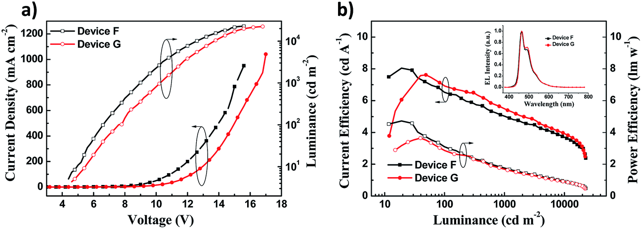 | ||
| Fig. 5 (a) J–V–L characteristics of devices F and G. (b) Current efficiency and power efficiency characteristics of devices F and G. The inset shows normalized EL spectra of devices F and G at 10 V. | ||
| Device | V on (V) | Emission peaksb (nm) | CIEx,yb | Current efficiencyc (cd A−1) | Power efficiencyc (lm W−1) |
|---|---|---|---|---|---|
| a Defined as onset voltage of log(J)–V curve. b At 10 V. c Values at 100 cd m−2, 1000 cd m−2, and 5000 cd m−2. | |||||
| F | 4.5 | 464, 492 | (0.15, 0.23) | 6.5/5.1/4.2 | 3.1/1.8/1.2 |
| G | 5.0 | 464, 492 | (0.15, 0.25) | 6.9/5.5/4.4 | 2.9/1.7/1.1 |
In summary, a green organic semiconductor material DSFX-TFB was synthesized via a relatively green tandem reaction and direct arylation with PASE. Subsequently, the nondoped deep-blue OLEDs based on DSFX-TFB with high performance were successfully realized. The devices exhibited a maximum EQE of 4.1% and deep-blue emission with CIE coordinates of (0.15, 0.08). Furthermore, DSFX-TFB can be used as a host for fluorescent OLEDs with the host–guest structure and better device performances with CE of 8.03 cd A−1 and PE of 4.62 lm W−1 are obtained. These results proved that SFX-based organic semiconductors that are obtained by concise and atom-economic synthesis will be able to meet green electronics and green chemistry requirements, as well as having potential in the field of organic electronics. And organic semiconductors synthesized via PASE routes will be potential advanced materials for eco-friendly devices.
3. Experimental section
3.1 Synthesis
:C, 82.95%; H, 3.73%; F, 9.37%. Found: C, 82.78; H, 3.67%, F, 9.42%.
3.2 Measurements
The NMR spectrum was recorded on a Bruker AV 400 MHz NMR spectrometer. Mass spectra were collected using a Microflex MALDI-TOF mass spectrometer (Bruker Daltonics, Germany). UV-Vis absorption and photoluminescence spectra were recorded with a Shimadzu UV-3600 and a Shimadzu RF-5301PC spectrophotometer, respectively. The fluorescence quantum yields in solution and in thin film were measured using 9,10-diphenyl anthracene as a reference. Differential scanning calorimetry (DSC) and thermogravimetric analyses (TGA) were performed on a Shimadzu DSC-60A and DTG-60H Instrument, respectively. Cyclic voltammetric (CV) studies were conducted using a CHI600C in a typical three-electrode cell with a platinum sheet working electrode, a platinum wire counter electrode, and a silver/silver nitrate (Ag/Ag+) reference electrode.3.3 Device fabrication
All devices were fabricated by means of vacuum deposition with ITO glass (10 Ω square−1) as the substrate. The ITO surface was scrubbed and ultrasonic cleaned sequentially with detergent, acetone, ethanol, and deionized water, and then treated in an ultraviolet-ozone chamber after drying in an oven. After the organic layers were thermally deposited under a vacuum (about 4.0 × 10⁻⁴ Pa) at a rate of 1–2 Å s−1, 100 nm-thick Al was covered directly on the organic layers serving as the cathode. The cathode area defined an active device area of 2 × 2 mm2 through a shadow mask. The current–voltage–luminance (J–V–L) characteristics were measured with a PR-650 SpectraScan spectrometer and a Keithley 2400 programmable voltage–current source. All experiments and measurements were carried out at room temperature under ambient conditions.3.4 Theoretical computation methods
Geometrical optimization for the ground and excited states was carried out at the B3LYP/6-31G and CIS/6-31G levels, respectively. The TDDFT/B3LYP/6-31g calculations of the excitation energies were then performed at the optimized geometries. All the quantum-chemical calculations were performed using the Gaussian09 suite of programs.Acknowledgements
We would like to express our sincere gratitude to the following sources for financial assistance: National Natural Science Fund for Excellent Young Scholars (21322402), National Natural Science Foundation of China (U1301243, 21373114, 21274064, 21144004, 60876010, 61177029, 20974046, 61136003), Program for New Century Excellent Talents in University (NCET-11-0992), Ministry of Education Doctoral Fund of China (20133223110007), Science and Technology Innovation Team of Jiangsu Higher Education Institutions (2013), Natural Science Foundation of Jiangsu Province (BK2011761, BK2008053, SJ209003, BM2012010), Priority Academic Program Development of Jiangsu Higher Education Institutions, PAPD (YX03001), and Fundamental Research Funding for Central Universities (2572014BB21). We are grateful for the assistance of Professor Hong-Mei Zhang and graduate student Ran Bi.Notes and references
- L.-H. Xie, C.-R. Yin, W.-Y. Lai, Q.-L. Fan and W. Huang, Prog. Polym. Sci., 2012, 37, 1192 CrossRef CAS PubMed.
- C.-J. Li and B. M. Trost, Proc. Natl. Acad. Sci. U. S. A., 2008, 105, 13197 CrossRef CAS PubMed.
- J. C. Warner, A. S. Cannon and K. M. Dye, Environ. Impact Assess. Rev., 2004, 24, 775 CrossRef PubMed.
- D. S. Argyropoulos, et al., in Materials, Chemicals and Energy from Forest Biomass, ed. ACS Symposium Series 954, American Chemical Society, Washington, DC, 2007 Search PubMed.
- P. Anastas and N. Eghbali, Chem. Soc. Rev., 2010, 39, 301 RSC.
- P. T. Anastas and J. C. Warner, in Green Chemistry: Theory and Practice, Oxford University Press, New York, 1998, p. 30 Search PubMed.
- Z.-Q. Lin, J. Liang, P.-J. Sun, F. Liu, Y.-Y. Tay, M.-D. Yi, K. Peng, X.-H. Xia, L.-H. Xie, X.-H. Zhou, J.-F. Zhao and W. Huang, Adv. Mater., 2013, 25, 3664 CrossRef CAS PubMed.
- M. Irimia-Vladu, Chem. Soc. Rev., 2014, 43, 588 RSC.
- P. A. Clarke, S. Santos and W. H. C. Martin, Green Chem., 2007, 9, 438 RSC.
- M. E. Mowery and P. DeShong, J. Org. Chem., 1999, 64, 1684 CrossRef CAS PubMed.
- K. Goldberg and A. S. Goldman, in Activation and Functionalization of C–H Bonds, ACS Symposium Series, Oxford University Press, 2004 Search PubMed.
- D. Alberico, M. E. Scott and M. Lautens, Chem. Rev., 2007, 107, 174 CrossRef CAS PubMed.
- K. Okamoto, J. Zhang, J. B. Housekeeper, S. R. Marder and C. K. Luscombe, Macromolecules, 2013, 46, 8059 CrossRef CAS.
- D. J. Schipper and K. Fagnou, Chem. Mater., 2011, 23, 1594 CrossRef CAS.
- J. Zhang, W. Chen, A. J. Rojas, E. V. Jucov, T. V. Timofeeva, T. C. Parker, S. Barlow and S. R. Marder, J. Am. Chem. Soc., 2013, 135, 16376 CrossRef CAS PubMed.
- R. Che, Z. Wu, Z. Li, H. Xiang and X. Zhou, Chem.–Eur. J., 2014, 20, 7258 CrossRef CAS PubMed.
- N. Hall, Science, 1994, 266, 32 CAS.
- L.-H. Xie, F. Liu, C. Tang, X.-Y. Hou, Y.-R. Hua, Q.-L. Fan and W. Huang, Org. Lett., 2006, 8, 2787 CrossRef CAS PubMed.
- L. F. Tietze, Chem. Rev., 1996, 96, 115 CrossRef CAS PubMed.
- L.-H. Xie, J. Liang, J. Song, C.-R. Yin and W. Huang, Curr. Org. Chem., 2010, 14, 2169 CrossRef CAS.
- G. H. Posner, Chem. Rev., 1986, 86, 831 CrossRef CAS.
- B. B. Toure and D. G. Hall, Chem. Rev., 2009, 109, 4439 CrossRef CAS PubMed.
- A. R. Siamaki, M. Sakalauskas and B. A. Arndtsen, Angew. Chem., Int. Ed., 2011, 50, 6552 CrossRef CAS PubMed.
- F. Liu, L.-H. Xie, C. Tang, J. Liang, Q.-Q. Chen, B. Peng, W. Wei, Y. Cao and W. Huang, Org. Lett., 2009, 11, 3850 CrossRef CAS PubMed.
- J.-F. Gu, G.-H. Xie, L. Zhang, S.-F. Chen, Z.-Q. Lin, Z.-S. Zhang, J.-F. Zhao, L.-H. Xie, C. Tang, Y. Zhao, S.-Y. Liu and W. Huang, J. Phys. Chem. Lett., 2010, 1, 2849 CrossRef CAS.
- Z.-Q. Lin, P.-J. Sun, Y.-Y. Tay, J. Liang, Y. Liu, N.-E. Shi, L.-H. Xie, M.-D. Yi, Y. Qian, Q.-L. Fan, H. Zhang, H. H. Hng, J. Ma, Q. Zhang and W. Huang, ACS Nano, 2012, 6, 5309 CrossRef CAS PubMed.
- X.-H. Zhao, G.-H. Xie, Z.-D. Liu, W.-J. Li, M.-d. Yi, L.-H. Xie, C.-P. Hu, R. Zhu, Q. Zhao, Y. Zhao, J.-F. Zhao, Y. Qian and W. Huang, Chem. Commun., 2012, 48, 3854 RSC.
- J. E. Anthony, A. Facchetti, M. Heeney, S. R. Marder and X. Zhan, Adv. Mater., 2010, 22, 3876 CrossRef CAS PubMed.
- T. Zhang, R. Wang, H. Ren, Z. Chen and J. Li, Polymer, 2012, 53, 1529 CrossRef CAS PubMed.
- U. Giovanella, C. Botta, F. Galeotti, B. Vercelli, S. Battiato and M. Pasini, J. Mater. Chem. C, 2013, 1, 5322 RSC.
- H.-Q. Do and O. Daugulis, J. Am. Chem. Soc., 2008, 130, 1128 CrossRef CAS PubMed.
- D. Lapointe and K. Fagnou, Chem. Lett., 2010, 39, 1118 CrossRef.
- W. Lu, J. Kuwabara and T. Kanbara, Macromolecules, 2011, 44, 1252 CrossRef CAS.
- W. Lu, J. Kuwabara, T. Iijima, H. Higashimura, H. Hayashi and T. Kanbara, Macromolecules, 2012, 45, 4128 CrossRef CAS.
- S. A. Johnson, C. W. Huff, F. Mustafa and M. Saliba, J. Am. Chem. Soc., 2008, 130, 17278 CrossRef CAS PubMed.
- T. Huang, X. Wang, T. Malmgren, K. Hong and J. W. Mays, Macromol. Chem. Phys., 2012, 213, 49 CrossRef CAS.
- J. H. Oh, S. Liu, Z. Bao, R. Schmidt and F. Würthner, Appl. Phys. Lett., 2007, 91, 212107-1 Search PubMed.
- H.-G. Jeong, B. Lim, D. Khim, M. Han, J. Lee, J. Kim, J.-M. Yun, K. Cho, J.-W. Park and D.-Y. Kim, Adv. Mater., 2013, 25, 6416 CrossRef CAS PubMed.
- H. M. Zhang, W. C. H. Choy and K. Li, IEEE Trans. Electron Devices, 2010, 57, 125 CrossRef CAS.
- S. Z. Yue, S. M. Zhang, Z. S. Zhang, Y. K. Wu, P. Wang, R. D. Guo, Y. Chen, D. L. Qu, Q. Y. Wu, Y. Zhao and S. Y. Liu, J. Lumin., 2013, 143, 619 CrossRef CAS PubMed.
- S.-O. Jeon, Y.-M. Jeon, J.-W. Kim, C.-W. Lee and M.-S. Gong, Synth. Met., 2007, 157, 558 CrossRef CAS PubMed.
- H. Khizar ul, M. A. Khan, X. Y. Jiang, Z. L. Zhang, X. W. Zhang, B. Wei, J. M. Wei, L. Zhang and J. Li, J. Lumin., 2009, 129, 1158 CrossRef PubMed.
Footnote |
| † Electronic supplementary information (ESI) available. See DOI: 10.1039/c4tc01963f |
| This journal is © The Royal Society of Chemistry 2015 |