
 Open Access Article
 This Open Access Article is licensed under a
 Creative Commons Attribution 3.0 Unported Licence
UV-assisted synthesis of indium nitride nano and microstructures†
Mahalieo
Kao
ab,
Rudolph M.
Erasmus
bd,
Nosipho
Moloto
a,
Neil J.
Coville
*ab and
Sabelo D.
Mhlanga
*bc
aMolecular Sciences Institute, School of Chemistry, University of the Witwatersrand, Johannesburg 2050, South Africa. E-mail: Neil.coville@wits.ac.za
bDST-NRF Centre of Excellence in Strong Materials, University of the Witwatersrand, Johannesburg 2050, South Africa
cNanotechnology and Water Sustainability Research Unit, College of Science, Engineering and Technology, University of South Africa, Florida Science Campus, Johannesburg, South Africa. E-mail: mhlansd@unisa.ac.za
dRaman and Luminescence Laboratory, School of Physics, University of the Witwatersrand, Johannesburg 2050, South Africa
First published on 9th February 2015
Abstract
Indium nitride (InN) has been made the first time by a combined thermal/UV photo-assisted process. Indium oxide (In2O3) was reacted with ammonia using two different procedures in which either the ammonia was photolysed or both In2O3 and ammonia were photolysed. A wide range of InN structures were made by these procedures that were determined by the reaction conditions (time, temperature). The reaction of In2O3 with photolysed NH3 gave InN rod-like structures that were made of stacked cones (6 h/750 °C) or discs (6 h/800 °C) and that contained some In2O3 residue. In contrast, photolysis of both In2O3 and NH3 gave InN nanowires and pure InN nanotubes filled with In metal (>90%). The transformation of the 3D In2O3 particles to the tubular 1D InN was monitored as a function of time (1–4 h) and temperature (700–800 °C); the product formed was very sensitive to temperature. The band gap of the In filled InN nanotubes was found to be 1.89 eV.
1 Introduction
InN is an understudied material because it is difficult to produce due to its low decomposition temperature and its high equilibrium pressure with N2.1 This has led to many controversies about the properties of this material. The inconsistencies and lack of reproducibility observed in the reported syntheses for this material escalates the problem.InN has been grown with morphologies that range from one dimension (1D) to three dimensions (3D).2,3 1D nanostructures are of particular importance in nanoscience and nanotechnology since they can be used to control space-confined transport phenomena,4,5 exhibit a discrete density of states and at the same time maintain a continuous transport path.6 They are of great importance in the understanding of the fundamental properties of low dimensional systems, and for use in potential nanodevice applications.7
Chemical vapour deposition (CVD) has proven to be a feasible method to prepare 1D InN nanomaterials.8–11 Temperature has been identified as a driving force that determines the different types of morphologies of the 1D InN nanostructures synthesised by CVD.11–13 The many studies reported on the synthesis of 1D InN using CVD have related to InN nanowires while much less work has been done on the synthesis of InN nanotubes.7,10–12,14
In2O3 is very attractive as an indium source in CVD studies due to the ease with which it can be handled. Body centred cubic In2O3 with space group Ia3 has a direct band gap and dominant ionic bonding.15 The magnitudes of the absorption and reflection coefficients for In2O3 are low, in the energy range 0–5 eV, indicating transparency in the material.15 It has a band gap of 3.6 eV.16
Several CVD studies have reported on the use of In2O3 for the preparation of InN. Zhang et al. reported the synthesis of InN nanowires through nitridation of a mixture of In metal and In2O3 (mole ratio 4![[thin space (1/6-em)]](https://www.rsc.org/images/entities/char_2009.gif) :1) at 700 °C for a reaction time of 4 h in NH3.8 However the XRD pattern of the InN showed the existence of an oxide impurity. On the other hand Tang et al. have reported the preparation of single crystal InN nanowires by nitriding a mixture of In metal and In2O3 (mole ratio ∼5:1) at 525 °C for a period of 30 min under NH3, based on a SAED pattern of a hexagonal crystal system and Raman spectroscopy.9 At the other extreme, carbonitridation of In2O3via CVD for 1.5 h was reported to give InN nanowires at 1150–1180 °C and InN nanotubes at 1190–1220 °C.14 Gao et al. reported complete nitridation of nanosized In2O3 and In(OH)3 powders within 8 h at 600 °C under NH3.17 In contrast, Luo et al. have reported several studies on the synthesis of InN and reported complete conversion of In2O3 powder to InN nanowires at 700 °C for a reaction period of 8 h in NH3 whereas for a shorter time period (4 h) oxide impurities were noted in their study.18 In a related study, done by a different group, a change in dimensionality on nitridation of In2O3 (650–700 °C for 4 h), was reported.11 Dimensional and structural evolution from 1D InN nanowires to 2D InN plates was achieved through temperature increments of 25 °C.11 Luo et al. also reported on the impact of reaction time on the morphologies of structures resulting from nitridation of In2O3 at 680 °C in the presence of a gold catalyst. In this study, both InN nanowires (14 h) and InN nanobelts (38 h) were produced.19 In yet another study at, 680 °C, Luo et al. made pure InN nanobelts (22 h); microtubes coexisting with nanobelts after 26 h, but after 30 h microtubes dominated.10 It has also been reported that a dramatic change in InN morphology with temperature indicated predominant involvement of In2O gas, formed from the decomposition of In2O3, in the growth of InN structures.12
:1) at 700 °C for a reaction time of 4 h in NH3.8 However the XRD pattern of the InN showed the existence of an oxide impurity. On the other hand Tang et al. have reported the preparation of single crystal InN nanowires by nitriding a mixture of In metal and In2O3 (mole ratio ∼5:1) at 525 °C for a period of 30 min under NH3, based on a SAED pattern of a hexagonal crystal system and Raman spectroscopy.9 At the other extreme, carbonitridation of In2O3via CVD for 1.5 h was reported to give InN nanowires at 1150–1180 °C and InN nanotubes at 1190–1220 °C.14 Gao et al. reported complete nitridation of nanosized In2O3 and In(OH)3 powders within 8 h at 600 °C under NH3.17 In contrast, Luo et al. have reported several studies on the synthesis of InN and reported complete conversion of In2O3 powder to InN nanowires at 700 °C for a reaction period of 8 h in NH3 whereas for a shorter time period (4 h) oxide impurities were noted in their study.18 In a related study, done by a different group, a change in dimensionality on nitridation of In2O3 (650–700 °C for 4 h), was reported.11 Dimensional and structural evolution from 1D InN nanowires to 2D InN plates was achieved through temperature increments of 25 °C.11 Luo et al. also reported on the impact of reaction time on the morphologies of structures resulting from nitridation of In2O3 at 680 °C in the presence of a gold catalyst. In this study, both InN nanowires (14 h) and InN nanobelts (38 h) were produced.19 In yet another study at, 680 °C, Luo et al. made pure InN nanobelts (22 h); microtubes coexisting with nanobelts after 26 h, but after 30 h microtubes dominated.10 It has also been reported that a dramatic change in InN morphology with temperature indicated predominant involvement of In2O gas, formed from the decomposition of In2O3, in the growth of InN structures.12
It can be seen from the studies mentioned that the standard reaction parameters for the synthesis of InN tubes from In2O3 have not yet been confirmed and agreed upon. The reported reaction parameters show wide ranges involving a single parameter such as the type of nitrogen source (N2, NH3), the flow rate (30–500 sccm), the time of reaction (1½–30 h) and the temperature (680–1220 °C).7,10–12,14 More than two thirds of the reported InN tubes are in the micrometer scale and the longest InN tubes reported are several microns in length.7
This study reports on the first UV photochemical synthesis of a range of InN structures as well as partially filled indium nitride nanotubes by photo-assisted nitridation of In2O3 in NH3. Photo-assisted reactions are typically done with lasers due to their high peak intensities.20 However, UV-photochemical vapour deposition (UV-CVD) has been successfully used in the past to deposit numerous metals, insulators, and semiconducting films.21–23 In photochemical reactions, absorption of light by a reactant molecule enables an inaccessible reaction path to occur by bringing the reactants to the necessary activation energy and also by changing the symmetry of the reactant's electronic configuration.24 Medium pressure mercury UV lamps are important radiation sources for photochemical applications. When medium pressure mercury lamps are used more energy levels are excited resulting in more spectral lines as well as a continuum due to recombination radiation.25 The major UV spectral lines emitted by these lamps are at 254 nm (4.8 eV) and 185 nm (6.7 eV). The majority of the UV-photochemical studies reported to date has focused on the deposition of two dimensional (2D) structures (i.e. thin films).26 Most films are normally produced using plasma deposition techniques in glow discharge.
UV-photochemical deposition of 1D group III-nitride nanostructures, with NH3, is not well established. Boron nitride nanotubes were synthesized by using excimer laser ablation at 1200 °C in different carrier gases.27 A few UV-synthesis studies have been reported on 1D gallium nitride (GaN) nanostructures. Shi et al. reported on GaN nanowires made from gallium oxide, using an excimer pulsed laser.28 Lieber and Duan also synthesised GaN nanowires by laser ablation of a metal containing target.29 There are however, to our knowledge, no studies reported on UV-CVD synthesis of one dimensional (1D) III-nitrides in general, and specifically on indium nitride (InN).
2 Results and discussion
2.1 InN synthesis by photolysis of only NH3
The effect of photo-activating only the ammonia in the nitridation of In2O3, was investigated by placing a boat containing In2O3 downstream out of the UV-light (i.e. the sample was protected from the UV light) (Fig. 1, position 1). In the absence of photolysis and using this configuration, (T > 700 °C) no InN was formed. Also, photolysis performed below 700 °C, yielded no InN. This is to be contrasted with reports on the production of InN at much lower temperatures using plasma assisted CVD.30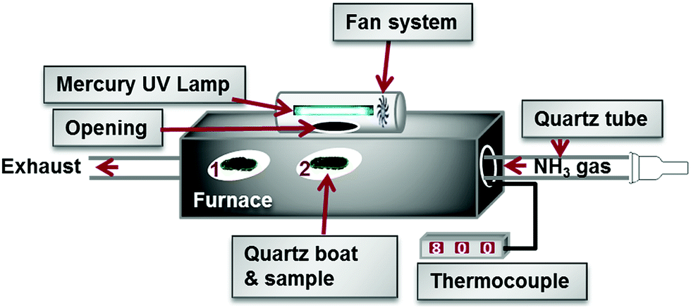 | ||
| Fig. 1 A horizontal CVD furnace with a mercury UV lamp housing equipped with a cooling fan system. Position 1 is the position where NH3 was irradiated but the quartz boat and its contents were not irradiated by UV-light. Position 2 marks the position where the NH3, the quartz boat and its contents are illuminated by the UV-light. | ||
Reactions involving the photolysis of NH3 in position 1 (Fig. 1) were also performed for 6 h at 700, 750 and 800 °C and soft black powders or dark brown fluffy materials were produced and collected from the quartz boat. In reactions performed for shorter times, the product was dominated by In2O3 (see Table S1†).
The XRD patterns of the as-synthesised materials made at 700–800 °C (Fig. S1†) revealed that after 6 h wurtzite InN was formed in all reactions but the product contained varying amounts of In2O3. XRD analysis showed that In2O3 in the product did not decrease substantially with increasing temperature as one might expect. Microscopy analysis also revealed that the indium oxide signals found in the InN XRD pattern are due to large residual In2O3 particles which did not completely react; the residual In2O3 was not due to a residual oxide coating of the InN. For materials made at 800 °C after 6 h reaction, spherical droplets of metallic indium were also observed at the bottom of the quartz boat. The images shown in Fig. 2 correspond to InN structures and indicate the variability in InN morphologies formed by variation in temperature.
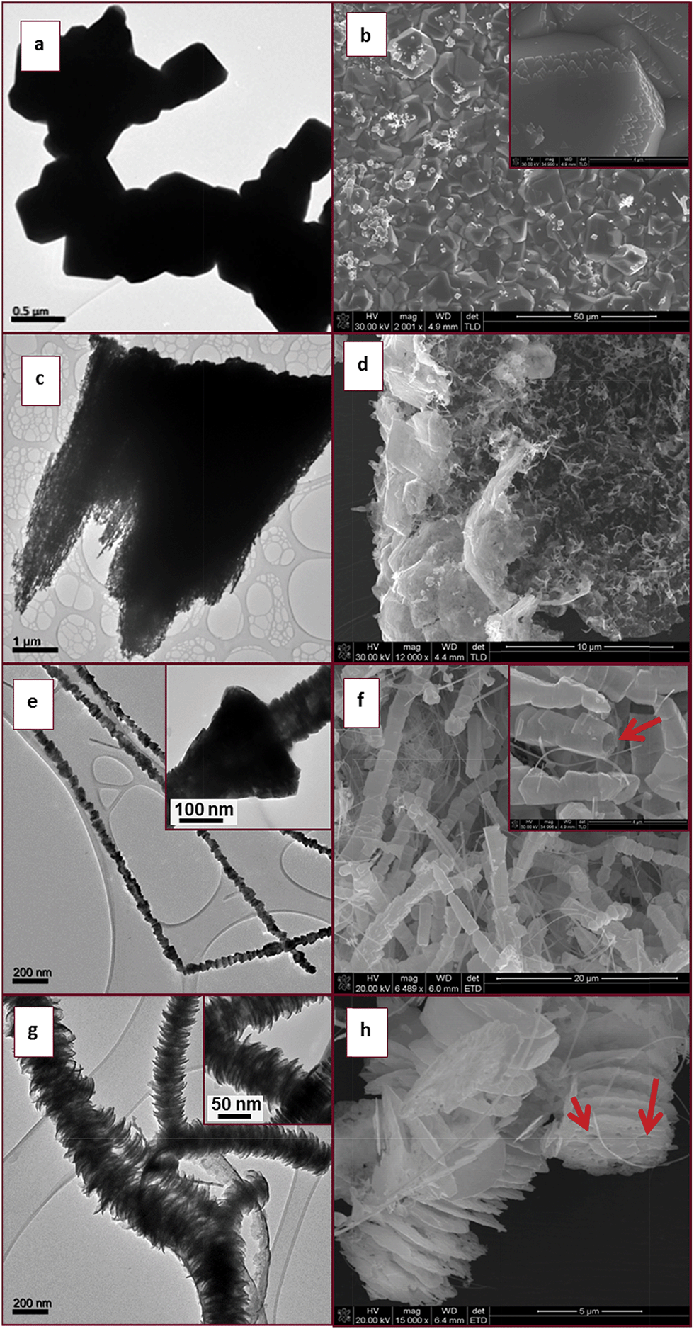 | ||
| Fig. 2 (a) TEM and (b) SEM images of as purchased In2O3 particles, (c) TEM and (d) SEM images of perforated materials formed at 700 °C, (e) TEM and (f) SEM images of segmented rod like structures at 750 °C (the arrow indicates the hollow core), (g) TEM and (h) SEM images of flaky structures at 800 °C (the arrows show perforations). All reactions were performed by photolysis of NH3 only. | ||
TEM and SEM images of the precursor In2O3 prior to reaction showed solid agglomerated well defined 3D facetted particles with varying dimensions (Fig. 2a and b). Higher magnification SEM images reveal that all the particle tips sticking out from the agglomerate have rhombohedral-like faces varying in size that depend on both the size of the parent particle and the extent it is embedded into the agglomerate (Fig. 2b insert). TEM and SEM analyses of the collected materials after 6 h at 700 °C showed that the product consisted of an irregularly perforated material (Fig. 2c and d). At 750 °C TEM and SEM images revealed that rod-like structures had formed (Fig. 2e and f). These rod-like structures possessed rough surfaces (Fig. 2e). High magnification TEM analysis of the rod-like structures showed that the roughness is due to stacking of cone like pieces that form the overall structure (Fig. 2e insert). An arrow shows that some of the cones are actually hollow, an indication that the rod-like structures are tubular in nature (Fig. 2f insert).
At 800 °C SEM analysis revealed that unusual 1D structures were formed from stacked disc-like units (Fig. 2h). The flake-like nature of the stacked discs creates an illusion of a rod-like structure, as revealed by the high magnification TEM image (Fig. 2g insert). The flakes had a rough surface texture and arrows indicate some of the perforations on the surface of the flakes (Fig. 2h). This disc type of morphology has not been reported previously in the literature for InN nanostructures.
In summary, even though a 100% pure InN material was not synthesized from photolysis of only NH3, information on the structure generation as a function of temperature was obtained. We suggest that the In2O3 was etched by the species generated by photolysis of NH3 in the process of nitridation (in the absence of photolysis no InN was made under the reaction conditions studied). No oxide nanowires were observed but the parent oxide particles were observed. The species formed from NH3 degrade the oxide leading to formation of InN with a disc like appearance and with increased temperature these discs become longer and more flake like.
2.2 InN synthesis by photolysis of both indium oxide and NH3
 | ||
| Fig. 3 XRD patterns of wurtzite InN materials prepared from photolysis of In2O3 and NH3 in 2 h at different temperatures. | ||
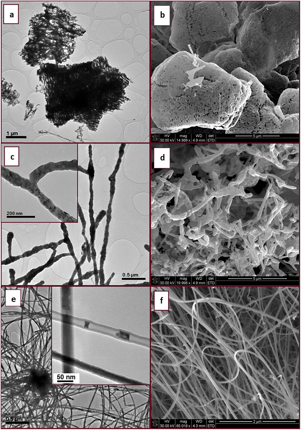 | ||
| Fig. 4 (a) TEM and (b) SEM images of porous InN particles showing irregular pores at 700 °C, (c) TEM and (d) SEM images of amorphous nanowires at 750 °C, (e) TEM and (f) SEM images of partially filled InN tubes at 800 °C. All reactions were held for 2 h at their respective temperatures. | ||
2.3 Photolysis of indium oxide and NH3 as a function of time
 | ||
| Fig. 5 XRD patterns of wurtzite InN materials prepared at 750 °C for different duration. | ||
 | ||
| Fig. 6 XRD patterns of the wurtzite InN product synthesised by photoactivation of In2O3 and NH3 at 800 °C as a function of time. | ||
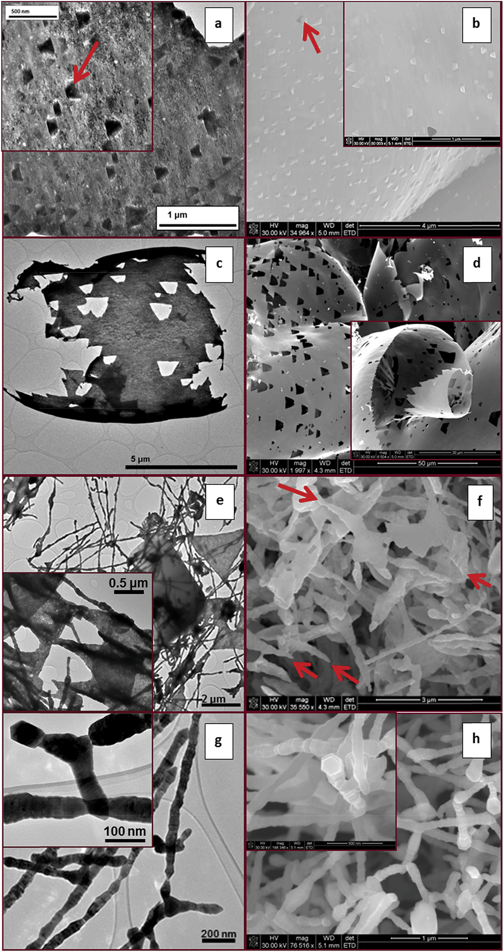 | ||
| Fig. 7 (a) TEM and (b) SEM images of 2D microsheets at 750 °C for 30 min; (c) TEM and (d) SEM images of perforated 2D microsheets at 750 °C for 1 h; (e) TEM and (f) SEM images of amorphous InN nanowires formed from 2D microsheets at 750 °C for 2 h; (g) TEM and (h) SEM images of InN nanowires at 750 °C for 3–4 h. | ||
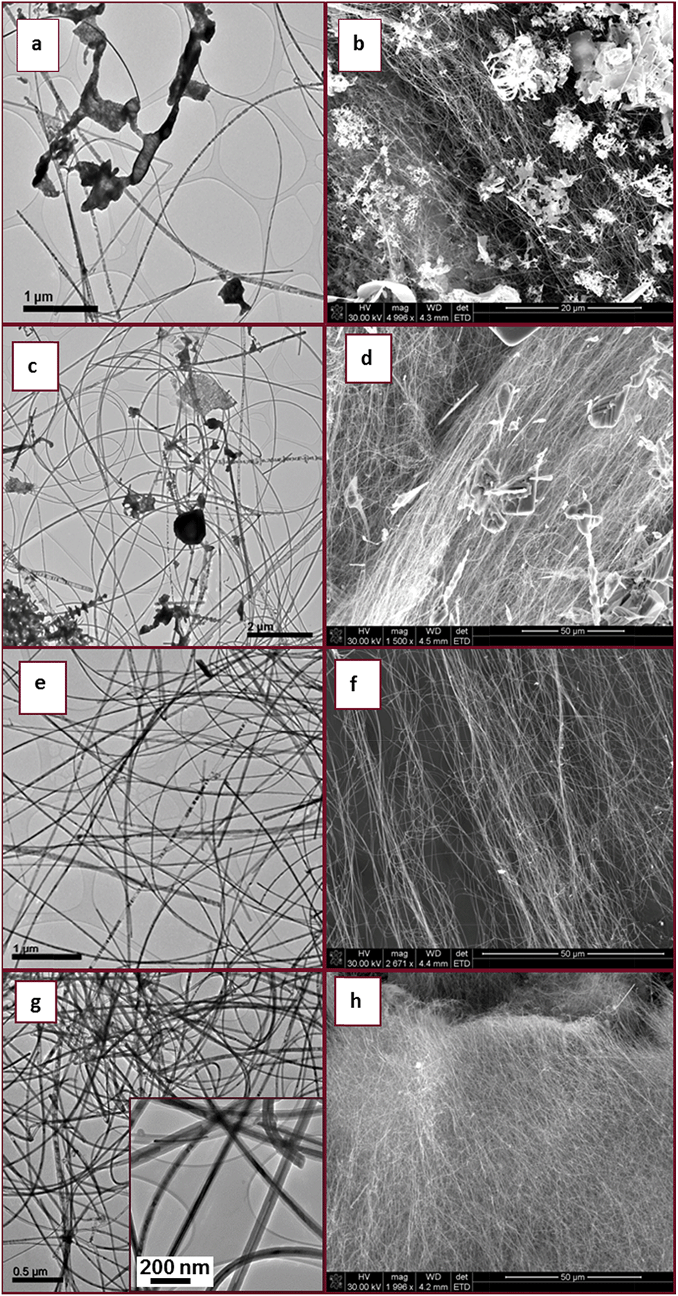 | ||
| Fig. 8 (a) TEM and (b) SEM images of InN nanotubes at 800 °C in 30 min. (c) TEM and (d) SEM images of the nanotubes at 800 °C for 1 h (e) TEM and (f) SEM images of the nanotubes at 800 °C for 3 h, (g) TEM and (h) SEM images of the nanotubes at 800 °C for 4 h. | ||
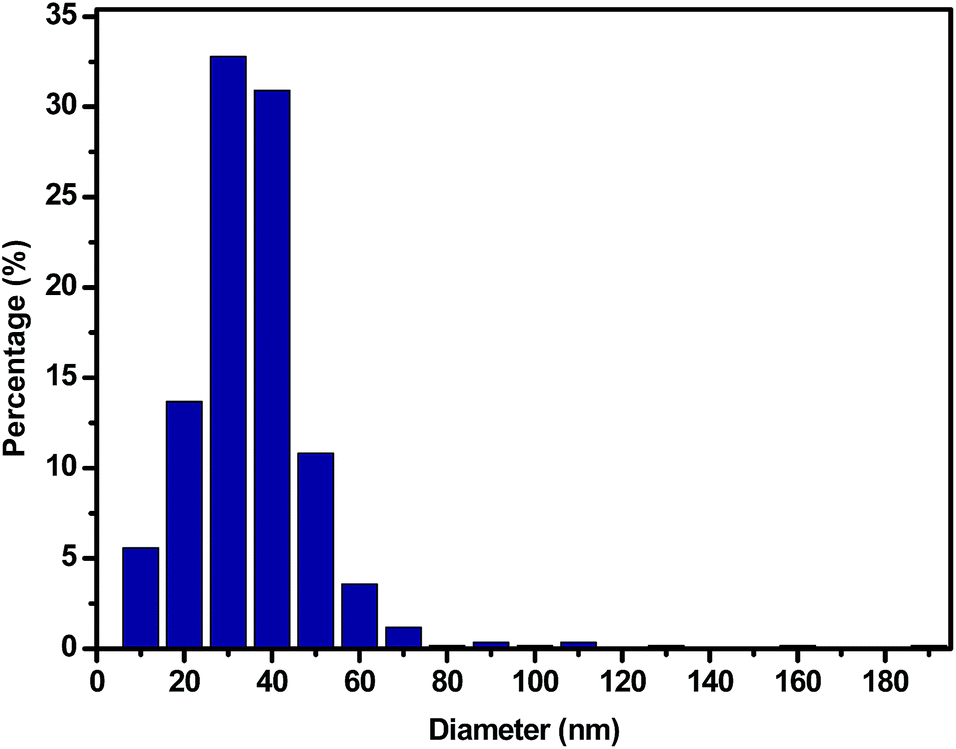 | ||
| Fig. 9 InN nanotube diameters obtained from TEM studies. | ||
To our knowledge indium filled InN nanotubes have not been previously reported. However, GaN nanotubes partially filled with indium have been achieved through indium assisted thermal evaporation. It was suggested that indium played an important role in the formation of nanotubes since spherical indium particles were found at the tips of the GaN tubes.31 We propose that InN nanotubes may develop from both 2D sheets and 3D microparticles as long as the reaction conditions generate an indium catalyst essential for tube formation. In our study the general quality and selectivity of the product (InN) improved gradually with increasing time of reaction.
2.4 Spectral properties of In filled InN nanotubes
Fig. 10 shows the Raman spectrum of the partially filled InN nanotubes made at 800 °C (2 h). The E2 high mode of the wurtzite InN is observed at 478 cm−1. The strain-free Raman frequency of the E2 high mode has been reported to be 490 cm−1 for wurtzite InN.32 Hence it is blue shifted relative to the reported position for strain free InN. Usually a shift to lower wavenumbers indicates the presence of tensile stress. The Raman peak at 581 cm−1 is also blue shifted (∼4 cm−1) relative to the A1 longitudinal optical (LO) mode reported at 585–590 cm−1.33 The data thus indicates tensile stress in the material.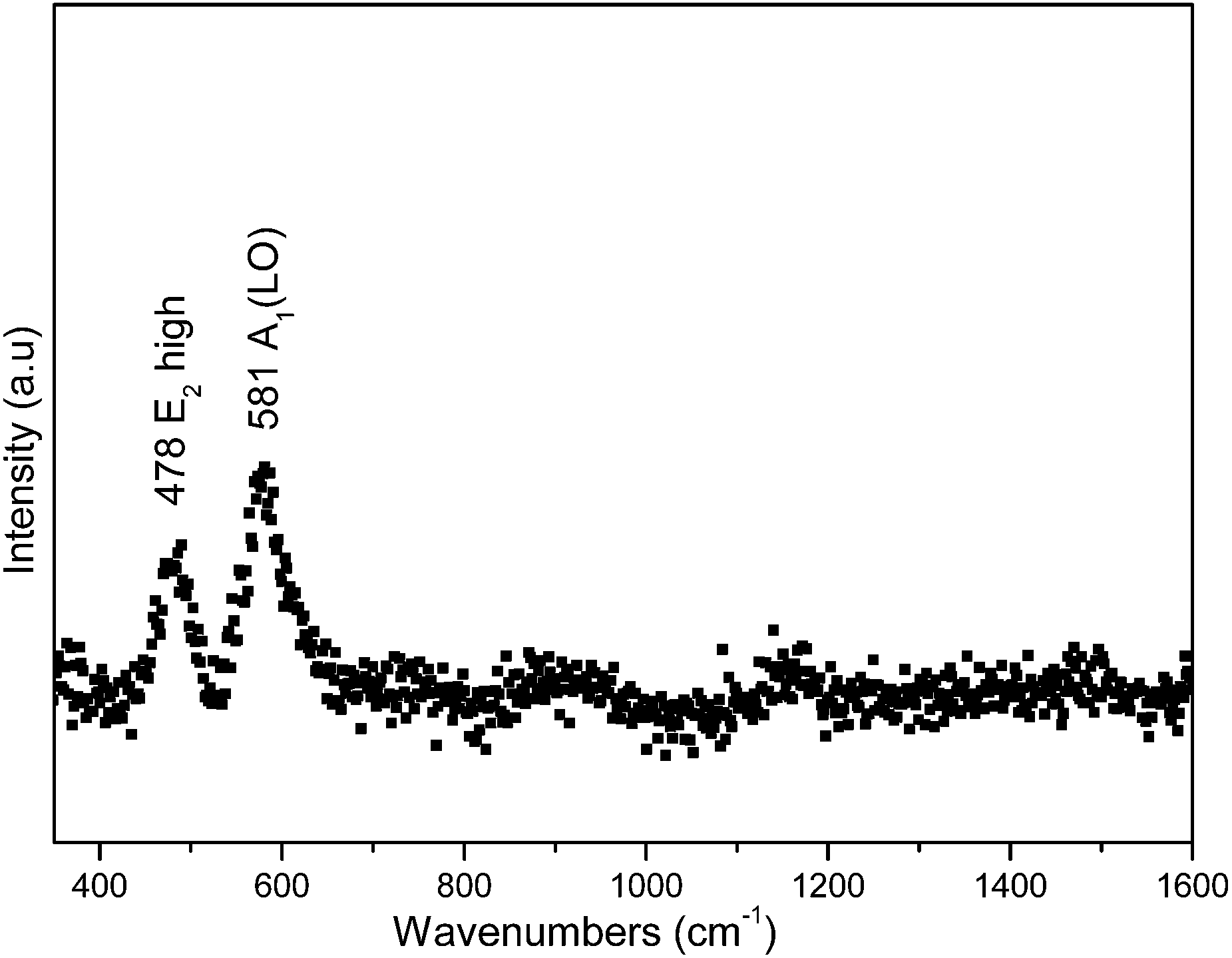 | ||
| Fig. 10 Raman spectrum of partially filled InN nanotubes made at 800 °C. | ||
The fundamental band gap value for InN is still a subject of controversy. The values from the reported data vary between 0.65 eV to 2.1 eV.34 Various phenomena, mechanisms and processes such as deep level traps, the Mie resonance, the Burstein–Moss effect, quantum confinement, oxygen incorporation and nitrogen-vacancies have been proposed to explain the band gap values measured for InN.34 It has also been shown that deviations in the In:N stoichiometric ratio can result in a large change in the band gap.35 Polycrystallinity has been identified as one of the factors that may lead to high band gap values. In InN materials polycrystallinity has been associated with excess nitrogen; and it has been suggested that excess nitrogen incorporation occurs largely when non-equilibrium growth techniques such as RF sputtering, and MBE are used.36
UV-vis/NIR diffuse reflectance spectroscopy was used in this study to determine the band gap value of the partially filled InN nanotubes made at 800 °C for 4 h. It has been suggested that the DRS technique can allow for the extraction of the band gap values of powder semiconductors without any ambiguity.37 The estimated band gap energy of partially filled tubes made at 800 °C was found to be 1.89 eV (Fig. 11 insert). This value is close to the original band gap data reported for InN (1.9 eV)38 but much larger than the more recent band gap values reported (0.7 eV) for InN.39 The observed band gap values might be influenced by the possible presence of defects suggested by tensile stress indicated by Raman analysis. It also might to some extent be influenced by the indium within the core of the nanotubes.34 The indium could increase the overall carrier concentration of the InN nanotubes. Large carrier concentrations have been correlated to high band gap values associated with the Burstein–Moss effect.40
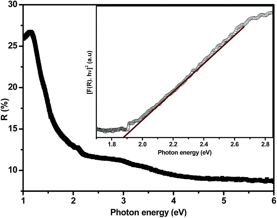 | ||
| Fig. 11 Diffuse reflectance spectra of partially filled InN nanotubes at 800 °C. The insert shows the Kubelka–Munk function analyses of the DRS of partially filled InN tubes at 800 °C. | ||
2.5 Reaction mechanism
It is interesting to note that the morphologies of the synthesized 1D InN nanostructures depend remarkably on small changes in the growth temperature. Ding et al. reported that in the vapour–liquid–solid (VLS) mechanism the shape of a 1D structure is determined by the interfacial lattice mismatch between a catalyst particle and a 1D structure.41 They however suggested that amongst other factors, temperature played a crucial role in determining the shape of a 1D structure but a detailed mechanism was not provided. Bando et al. and others suggested that in a vapour–solid (VS) mechanism, hollow InN nanotubes were formed by a diffusion-limited process at high temperatures, while the solid InN nanowires were formed by a kinetically limited process at lower temperatures in a VS mechanism.14,42,43The InN obtained from the reaction between In2O3 and NH3 generated by photo-activation of only NH3, showed a change in the morphology with time and temperature. All samples contained small amounts of In2O3. The photo-activated reaction of both In2O3 and NH3, as a function of temperature also gave rise to different morphologies of pure InN.
For all reactions in which only NH3 was photolysed, a minimum of 6 h appears necessary to obtain InN even though it was still impure. The morphologies varied with temperature indicating that the mechanism of formation is temperature dependent.
The TEM and SEM analyses shed some light into the progressive development of 1D morphologies of InN from 3D In2O3 particles. It is suspected that the porous particles form from the solid In2O3 particles by thermal decomposition in a manner similar to that proposed by Yu et al.44–46 This entails adsorption, diffusion and subsequent reaction of NH3 species on and within the In2O3 particle core. A InN shell would be formed from surface based reactions on the outside the In2O3 core, later converting to a porous hollow particle (Fig. S2†). The general reaction between In2O3 and NH3 proposed by several authors can explain the generation of H2O as a by-product.12,17,18,47 As decomposition of the In2O3 core proceeds in the presence of NH3, the generated H2O vapour accumulates in the core until the pressure, when high enough, weakens the shell of the particle generating tiny pores that allow the trapped gas to escape. Alternatively the pores could be formed by conversion of In2O3 to InN by NH3; in the process the structure changes, as N replaces O. This is to be contrasted with the mechanism proposed by Ashok and co-workers to interpret the synthesis of porous InN microcages. Ashok et al. observed porous microcages in the InN synthesis using a lower temperature (650 °C) and a shorter reaction time (1 h). They suggested that microcages form by self-assembly of a few web-like structures controlled by a diffusion limited process.48 In another study InN microtubes with holes were observed and it was suggested that the holes were formed as a result of a lack of InN vapour in the reaction feed.12
The kinetics and the reaction mechanism for the photochemical decomposition of ammonia by ultraviolet light has not yet been settled,49–51 and even in the simplest case of thermal NH3 decomposition several matters are still in dispute.52–54 However, both thermal and photochemical decomposition studies of NH3 have identified N2H4 as the molecular intermediate formed before conversion to H2 and N2 (molar ratio 3:1).50,52 NH3 and N2H4 are known for their etching properties. We therefore propose that the 2D microsheets observed in this study are formed from surface etching of the 3D In2O3 particle agglomerates by UV-light, NH3 and N2H4. Based on differences in the parent particle size as well as differences in exposure of the individual particles in the agglomerate, to the etching agents, some particles are selectively etched faster than others creating the 2D sheet with uneven points. As a result the particles least affected by etching remain stuck in the sheet creating mounds. Prolonged etching of the sheet creates weak points around the particles stuck in the parent sheet and the particles fall off the 2D sheet leaving behind rhombohedral holes on the 2D sheet. This is to be contrasted with the proposition made by Schwenzer et al.11 They suggested that 2D microplates were formed by degradation of the InN microtube walls. They also observed triangular shaped holes on the microtubes. Our study helps bring into focus the mechanism of formation for the triangular/rhombohedral shaped holes observed on the InN microtubes/sheets.
Further degradation of the porous 2D sheet results in selective growth of the InN nanowires from the corners of the pieces of the parent sheet in a manner similar to that described by Schwenzer et al.11 They observed that the corners of the triangles of 2D InN plates grow into nanowires. They suggested that the co-existence of nano and microstructures indicated that the structures do not form independently from In2O3 but rather go through different stages.11 It is to be noted that another research study argued that the local differences in the morphology of InN structures suggested the independent growth of InN nano and microstructures.12 The schematic presentation of our proposed mechanism for 1D InN growth is presented in Fig. 12. The mechanism of nanowire growth from 2D sheets is to be contrasted with the mechanism of nanowire growth from microcages proposed by Ashok et al.48
 | ||
| Fig. 12 Reaction mechanism showing etching effects due to both the UV and ammonia species. | ||
We believe that at high temperatures (≥750 °C) decomposition of NH3 produces reducing species (e.g. N2H4, H2) in high abundance relative to reactions at low temperature. The reduction of In2O3 into indium is then highly favoured. The resulting indium metal particles embedded or supported on the 3D particle or the 2D sheet, could serve as catalysts from which indium filled InN nanotubes grow. This is supported by experiments we performed by conventional thermal nitridation of In2O3 (not shown), where at high temperatures all the In2O3 is converted to metallic indium. Thus UV irradiation aids in activating the nitriding species at lower temperatures to limit complete conversion to indium metal.
3 Experimental
In2O3 powder (Aldrich, particle size 300–600 nm, 99.99% purity) was placed in a quartz boat (L: 25 mm, D: 8 mm) that had been cleaned in ethanol. The boat was then loaded into a long quartz tube (L: 800 mm, D: 20 mm) which was installed horizontally into a furnace. The furnace has an opening (D: 30 mm) that allowed light from a mercury UV lamp in to the mid-region of the furnace to illuminate the tube and its contents. A 400 Watt medium pressure mercury UV lamp (model no. 3040, Photochemical reactors Ltd) was situated in a housing equipped with a cooling system (Fig. 1).The quartz tube was degassed and purged with high-purity (99.999%) nitrogen. During the growth process, 400 sccm of NH3 (anhydrous, 99.999%) was introduced into the tube. The flow rate of NH3 was programmed and maintained at 400 sccm using a Brookes mass flow controller at atmospheric pressure. The exhaust NH3 was bubbled through an oil bubbler before being discharged into the atmosphere. The furnace was set to 700–800 °C (the temperature error, ±2 °C) and was held there for 1–6 h, then cooled to room temperature under NH3.
Two sets of synthesis experiments were carried out. In the first setup (position 1), In2O3 powder was not irradiated by the UV lamp to prevent secondary photolysis of the product (Fig. 1) while varying temperature. In the second setup (position 2), both reactants (In2O3 and NH3) were irradiated while varying the synthesis temperature and time (1–4 h). The breakdown of all the reactions and the reaction parameters varied is tabulated in Table S1 (ESI†). A fluffy wool-like grey product was generated at the surface of the quartz boat after nitriding the reactant. In a typical optimised experiment 0.2 g of In2O3 was used and 0.08 g of partially filled InN nanotubes was obtained. XRD data used for structural analysis was collected on a Bruker D2 diffractometer with CuKα radiation. Morphologies were evaluated by SEM (NOVA) and TEM (Tecnai T12). The optical properties of InN nanotubes were characterized by diffuse reflectance spectroscopy (Praying Mantis DRS Cary 500) and Raman spectroscopy (Jobin Yvon LabRAM).
4 Conclusions
In this study we have indicated the use of a combined thermal/UV photolysed approach to make InN materials with a wide range of shapes. Photolysis of the NH3 provides a method to activate the NH3 that in the presence of In2O3 replaces the O atoms by N atoms (a reduction reaction). In doing so the In2O3 structure converts from a 3D structure to a 1D tubular material. Secondary growth processes lead to the final structures observed. The InN material that makes the tubes does so by means of supersaturation and nucleation from the catalytic liquid indium metal phase via a VLS mechanism. The anisotropic alignment of the indium filled InN nanotubes seen in all SEM images is a typical feature of the VLS method. The rod-like structures made of cones as well as flaky rods could be formed by a VS mechanism.Photolysis of the In2O3 (as well as the NH3) results in the formation of completely different structures. In this case the replacement of the O in the In2O3 by N is aided by the photolysis process. Thus, the solid particles become porous on photolysis as the replacement reaction of O by N progresses (700 °C). With an increase in temperature (800 °C), a pure InN is formed as more indium filled InN tubes are formed. However, over-reduction occurs and indium metal now readily forms.
This study indicates the rich range of InN materials that is accessible by simple synthetic strategies. The study also indicates that the various structures are all linked together i.e. the structures form from each other. More work will be required to gain further insight into these shape/size transformation reactions. Whether the methodology can be extended to the synthesis of other metal nitride materials will need further experimentation.
Acknowledgements
The authors would like to thank the DST-NRF CoE in Strong Materials, the DST-IBSA Nanotechnology Project (80287) and the DST-NRF SA-India research initiative program (76517) for funding.References
- J. B. MacChesney, Mater. Res. Bull., 1970, 5, 783 CrossRef CAS.
- S. Vaddiraju, A. Mohite, A. Chin, M. Meyyappan, G. Sumanasekera, B. W. Alphenaar and M. K. Sunkara, Nano Lett., 2005, 5, 1625 CrossRef CAS PubMed.
- T. J. Kistenmacher and W. A. Bryden, Appl. Phys. Lett., 1991, 59, 1844 CrossRef CAS PubMed.
- Y. Xia, P. Yang, Y. Sun, Y. Wu, B. Mayers, B. Gates, Y. Yin, F. Kim and H. Yan, Adv. Mater., 2003, 15, 353 CrossRef CAS.
- C. N. R. Rao, F. L. Deepak, G. Gundiah and A. Govindaraj, Prog. Solid State Chem., 2003, 31, 5 CrossRef CAS PubMed.
- M.-S. Hu, W.-M. Wang, T. T. Chen, L.-S. Hong, C.-W. Chen, C.-C. Chen, Y.-F. Chen, K.-H. Chen and L.-C. Chen, Adv. Funct. Mater., 2006, 16, 537 CrossRef CAS.
- H. Xu, Z. Liu, X. Zhang and S. Hark, Appl. Phys. Lett., 2007, 90, 113105 CrossRef PubMed.
- J. Zhang, L. Zhang, X. Peng and X. Wang, J. Mater. Chem., 2002, 12, 802 RSC.
- T. Tang, S. Han, W. Jin, X. Liu, C. Li, D. Zhang, C. Zhou, B. Chen, J. Han and M. Meyyapan, J. Mater. Res., 2004, 19, 424 CrossRef.
- S. Luo, W. Zhou, W. Wang, Z. Zhang, L. Liu, X. Dou, J. Wang, X. Zhao, D. Liu and Y. Gao, Appl. Phys. Lett., 2005, 87, 063109 CrossRef PubMed.
- B. Schwenzer, L. Loeffler, R. Seshadri, S. Keller, F. F. Lange, S. P. DenBaars and U. K. Mishra, J. Mater. Chem., 2004, 14, 637 RSC.
- W. Jung, C. S. Ra and B. Min, Bull. Korean Chem. Soc., 2005, 26, 1354 CrossRef CAS.
- X. M. Cai, F. Ye, S. Y. Jing, D. P. Zhang, P. Fan and E. Q. Xie, Appl. Surf. Sci., 2008, 255, 2153 CrossRef CAS PubMed.
- L. W. Yin, Y. Bando, D. Golberg and M. S. Li, Adv. Mater., 2004, 16, 1833 CrossRef CAS.
- S. Z. Karazhanov, P. Ravindran, P. Vajeeston, A. Ulyashin, T. Finstad and H. Fjellvåg, Phys. Rev. B: Condens. Matter Mater. Phys., 2007, 76, 075129 CrossRef.
- R. Weiher and R. Ley, J. Appl. Phys., 1966, 37, 299 CrossRef CAS PubMed.
- L. Gao, Q. Zhang and J. Li, J. Mater. Chem., 2003, 13, 154 RSC.
- S. Luo, W. Zhou, Z. Zhang, L. Liu, X. Dou, J. Wang, X. Zhao, D. Liu, Y. Gao and L. Song, Small, 2005, 1, 1004 CrossRef CAS PubMed.
- S. Luo, W. Zhou, Z. Zhang, X. Dou, L. Liu, X. Zhao, D. Liu, L. Song, Y. Xiang and J. Zhou, Chem. Phys. Lett., 2005, 411, 361 CrossRef CAS PubMed.
- Y. Hirota and O. Mikami, Electron. Lett., 1985, 21, 77 CrossRef CAS.
- D. Ehrlich, R. Osgood Jr and T. Deutsch, J. Vac. Sci. Technol., 1982, 21, 23 CrossRef CAS.
- V. Donnelly, M. Geva, J. Long and R. Karlicek, Appl. Phys. Lett., 1984, 44, 951 CrossRef CAS PubMed.
- H. Ando, H. Inuzuka, M. Konagai and K. Takahashi, J. Appl. Phys., 1985, 58, 802 CrossRef CAS PubMed.
- G. J. Kavarnos and N. J. Turro, Chem. Rev., 1986, 86, 401 CrossRef CAS.
- B. Gellert and U. Kogelschatz, Appl. Phys. B, 1991, 52, 14 CrossRef.
- D. Ehrlich and R. Osgood Jr, Thin Solid Films, 1982, 90, 287 CrossRef CAS.
- D. Yu, X. Sun, C. Lee, I. Bello, S. Lee, H. Gu, K. Leung, G. Zhou, Z. Dong and Z. Zhang, Appl. Phys. Lett., 1998, 72, 1966 CrossRef CAS PubMed.
- W. Shi, Y. Zheng, N. Wang, C. Lee and S. Lee, Chem. Phys. Lett., 2001, 345, 377 CrossRef CAS.
- X. Duan and C. M. Lieber, J. Am. Chem. Soc., 2000, 122, 188 CrossRef CAS.
- Y.-K. Chang and F. C.-N. Hong, Mater. Lett., 2009, 63, 1855 CrossRef CAS PubMed.
- L.-W. Yin, Y. Bando, Y.-C. Zhu, D. Golberg and M.-S. Li, Appl. Phys. Lett., 2004, 84, 3912 CrossRef CAS PubMed.
- X. Wang, S.-B. Che, Y. Ishitani and A. Yoshikawa, Appl. Phys. Lett., 2006, 89, 171907 CrossRef PubMed.
- V. Y. Davydov and A. Klochikhin, Semiconductors, 2004, 38, 861 CrossRef CAS.
- K. Butcher and T. Tansley, Superlattices Microstruct., 2005, 38, 1 CrossRef CAS PubMed.
- A. E. Morales, E. S. Mora and U. Pal, Rev. Mex. Fis. S, 2007, 53, 18 CAS.
- K. Scott, A. Butcher, M. Wintrebert-Fouquet, P. P. T. Chen, K. E. Prince, H. Timmers, S. K. Shrestha, T. V. Shubina, S. V. Ivanov and R. Wuhrer, Phys. Status Solidi C, 2005, 2, 2263 CrossRef CAS.
- H. Timmers, S. K. Shrestha and A. P. Byrne, J. Cryst. Growth, 2004, 269, 50 CrossRef CAS PubMed.
- M. Yoshimoto, H. Yamamoto, W. Huang, H. Harima, J. Saraie, A. Chayahara and Y. Horino, Appl. Phys. Lett., 2003, 83, 3480 CrossRef CAS PubMed.
- T. Matsuoka, H. Okamoto, M. Nakao, H. Harima and E. Kurimoto, Appl. Phys. Lett., 2002, 81, 1246 CrossRef CAS PubMed.
- W. Walukiewicz, S. Li, J. Wu, K. Yu, J. Ager Iii, E. Haller, H. Lu and W. J. Schaff, J. Cryst. Growth, 2004, 269, 119 CrossRef CAS PubMed.
- Y. Ding, P. X. Gao and Z. L. Wang, J. Am. Chem. Soc., 2004, 126, 2066 CrossRef CAS PubMed.
- E. P. Bakkers and M. A. Verheijen, J. Am. Chem. Soc., 2003, 125, 3440 CrossRef CAS PubMed.
- L. W. Yin, Y. Bando, J. H. Zhan, M. S. Li and D. Golberg, Adv. Mater., 2005, 17, 1972 CrossRef CAS.
- H.-D. Yu, M. D. Regulacio, E. Ye and M.-Y. Han, Chem. Soc. Rev., 2013, 42, 6006 RSC.
- H.-D. Yu, Z.-Y. Zhang, K. Y. Win, J. Chan, S. H. Teoh and M.-Y. Han, Chem. Commun., 2010, 46, 6578 RSC.
- H. Yu, D. Wang and M.-Y. Han, J. Am. Chem. Soc., 2007, 129, 2333 CrossRef CAS PubMed.
- Z. Chen, Y. Li, J. Jiang, C. Cao, T. Xu, Q. Chen, X. Xu and H. Zhu, RSC Adv., 2012, 2, 6806 RSC.
- V. D. Ashok, T. Ghoshal and S. De, J. Phys. Chem. C, 2009, 113, 10967 CAS.
- J. A. Kaye and D. F. Strobel, Icarus, 1983, 54, 417 CrossRef CAS.
- E. O. Wiig and G. B. Kistiakowsky, J. Am. Chem. Soc., 1932, 54, 1806 CrossRef CAS.
- N. Dietz, M. Straßburg and V. Woods, J. Vac. Sci. Technol., A, 2005, 23, 1221 CAS.
- D. Dirtu, L. Odochian, A. Pui and I. Humelnicu, Cent. Eur. J. Chem., 2006, 4, 666 CrossRef CAS PubMed.
- J. C. Elgin and H. S. Taylor, J. Am. Chem. Soc., 1929, 51, 2059 CrossRef CAS.
- R. R. Wenner and A. O. Beckman, J. Am. Chem. Soc., 1932, 54, 2787 CrossRef CAS.
Footnote |
| † Electronic supplementary information (ESI) available: XRD patterns of InN materials with oxide impurities synthesised from a reaction of In2O3 with photolysed NH3 at different temperatures for a period of 6 h. See DOI: 10.1039/c4ta06848c |
| This journal is © The Royal Society of Chemistry 2015 |