
 Open Access Article
 This Open Access Article is licensed under a Creative Commons Attribution-Non Commercial 3.0 Unported Licence
Antimony sulfide as a light absorber in highly ordered, coaxial nanocylindrical arrays: preparation and integration into a photovoltaic device
Yanlin
Wu
a,
Loïc
Assaud
a,
Carola
Kryschi
a,
Boris
Capon
b,
Christophe
Detavernier
b,
Lionel
Santinacci
c and
Julien
Bachmann
*a
aDepartment of Chemistry and Pharmacy, Friedrich-Alexander University of Erlangen-Nürnberg, Egerlandstrasse 1, D-91058 Erlangen, Germany. E-mail: julien.bachmann@fau.de
bDepartment of Solid State Sciences, Ghent University, Krijgslaan 281/S1, B-9000 Ghent, Belgium
cAix Marseille Université, CNRS, CINaM UMR 7325, F-13288 Marseille, France
First published on 10th February 2015
Abstract
We demonstrate the preparation of functional ‘extremely thin absorber’ solar cells consisting of massively parallel arrays of nanocylindrical, coaxial n-TiO2/i-Sb2S3/p-CuSCN junctions. Anodic alumina is used as an inert template that provides ordered pores of 80 nm diameter and 1–50 μm length. Atomic layer deposition (ALD) then coats pores of up to 20 μm with thin layers of the electron conductor and the intrinsic light absorber. The crystallization of the initially amorphous Sb2S3 upon annealing is strongly promoted by an underlying crystalline TiO2 layer. After the remaining pore volume is filled with the hole conductor by solution evaporation, the resulting coaxial p-i-n junctions display stable diode and photodiode electrical characteristics. A recombination timescale of 40 ms is extracted from impedance spectroscopy in open circuit conditions, whereas transient absorption spectroscopy indicates that holes are extracted from Sb2S3 with a lifetime of 1 ns.
Introduction
Nanostructured ‘third-generation’ types of solar cells are meant to replace the costly materials of planar cells (needed for the extreme efficiency of either light absorption or charge transport) with inexpensive ones by exploiting the geometric parameters smartly.1–4 However, these systems have not reached the efficiencies of the planar cells yet. Part of the difficulty in the optimization of these cells resides in the lack of control over the structure of the interface, typically based on a colloidal oxide layer.5,6 A direct investigation of the device physics via systematic variation of well-defined individual geometric parameters would be possible in a semiconductor junction organized in parallel cylindrical nanostructures of tunable length and diameter.15 This paper demonstrates the preparation of such a coaxial nanocylindrical solar cell, the principle of which is illustrated in Scheme 1.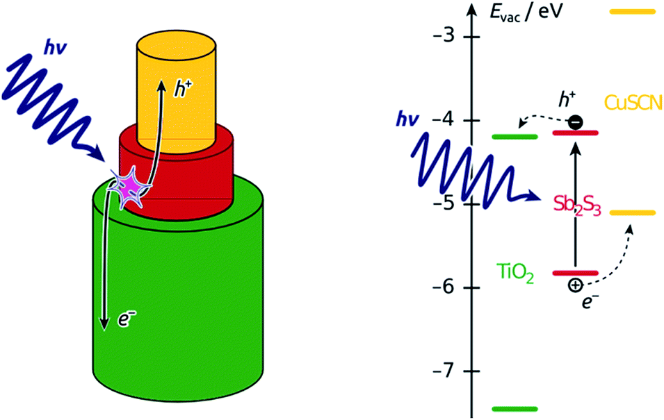 | ||
| Scheme 1 Function principle of the coaxial nanocylindrical solar cell. Left, schematic view of the geometry of one individual coaxial p-i-n junction amongst the large numbers of parallel cylinders constituting the solar cell device. Right, band diagram of the semiconductors involved.7–14 | ||
We focus on the so-called extremely thin absorber (ETA) cell, also described as a solid dye-sensitized cell (sDSSC). In ETA cells, a very thin intrinsic layer of strongly absorbing, inorganic solid (typically a II–VI or V2–VI3 semiconductor, such as CdSe, In2S3 or Sb2S3) is combined with solid electron and hole conductors, such as n-TiO2 and p-CuSCN, respectively.16,17 We propose a general preparative strategy based on coating the ordered, cylindrical nanopores of ‘anodic’ alumina (used as the template) with consecutive layers of the functional materials. To this goal, we use atomic layer deposition (ALD) as the crucial method that enables the experimentalist to coat thin layers on porous substrates with the following properties: (a) homogeneous deposition along the length of deep pores; (b) accurate tuning of the thickness deposited between 1 and 20 nm approximately; (c) high quality of the material, in particular accurate stoichiometry and absence of unwanted oxide.18–21 We have previously demonstrated that ALD is applicable to the deposition of Sb2S3 as the light absorber of ETA cells based on colloidal TiO2 crystals.22 We now have characterized the ALD of Sb2S3 in pores, investigated the necessary post-deposition treatment, and quantified some of the photovoltaic parameters of the functional device based on the nanocylindrical geometry. Our results establish a versatile preparative strategy towards the elusive ‘nanorod’ or ‘interdigitated’ solar cell.
Results and discussion
ALD-based Sb2S3 nanotube preparation: structure and tunability
The overall preparative procedure foreseen for our ordered arrays of nanocylindrical, coaxial p-i-n junctions as ETA solar cells is presented in Scheme 2. The preparation bases on mostly published individual steps. The two-step anodization of Al in oxalic acid provides an inert matrix the pores of which are ordered with a period of 105 nm (±10%) and pore diameter (after pore widening) 80 nm (±10%).1,23 We note that with these parameters, only 47% of the sample's total volume is taken up by the matrix. The remaining can be filled with the functional materials. This is performed by atomic layer deposition (ALD)18 and evaporative infiltration.2 The thin film technique ALD possesses the unique ability of coating complex substrates conformally, especially highly porous ones.24 In particular, it has been exploited for n-TiO2 layers in similar geometries in the context of dye-sensitized solar cells already.25 The Sb2S3 ALD procedure26,27 delivers a material of high quality (purity and stoichiometry) applicable to photovoltaic applications,22,28 which can even grow epitaxially near room temperature given an appropriate substrate.29 However, its capability to coat deep pores has not been investigated to date. Therefore, we will start with an extensive characterization of the Sb2S3 layers.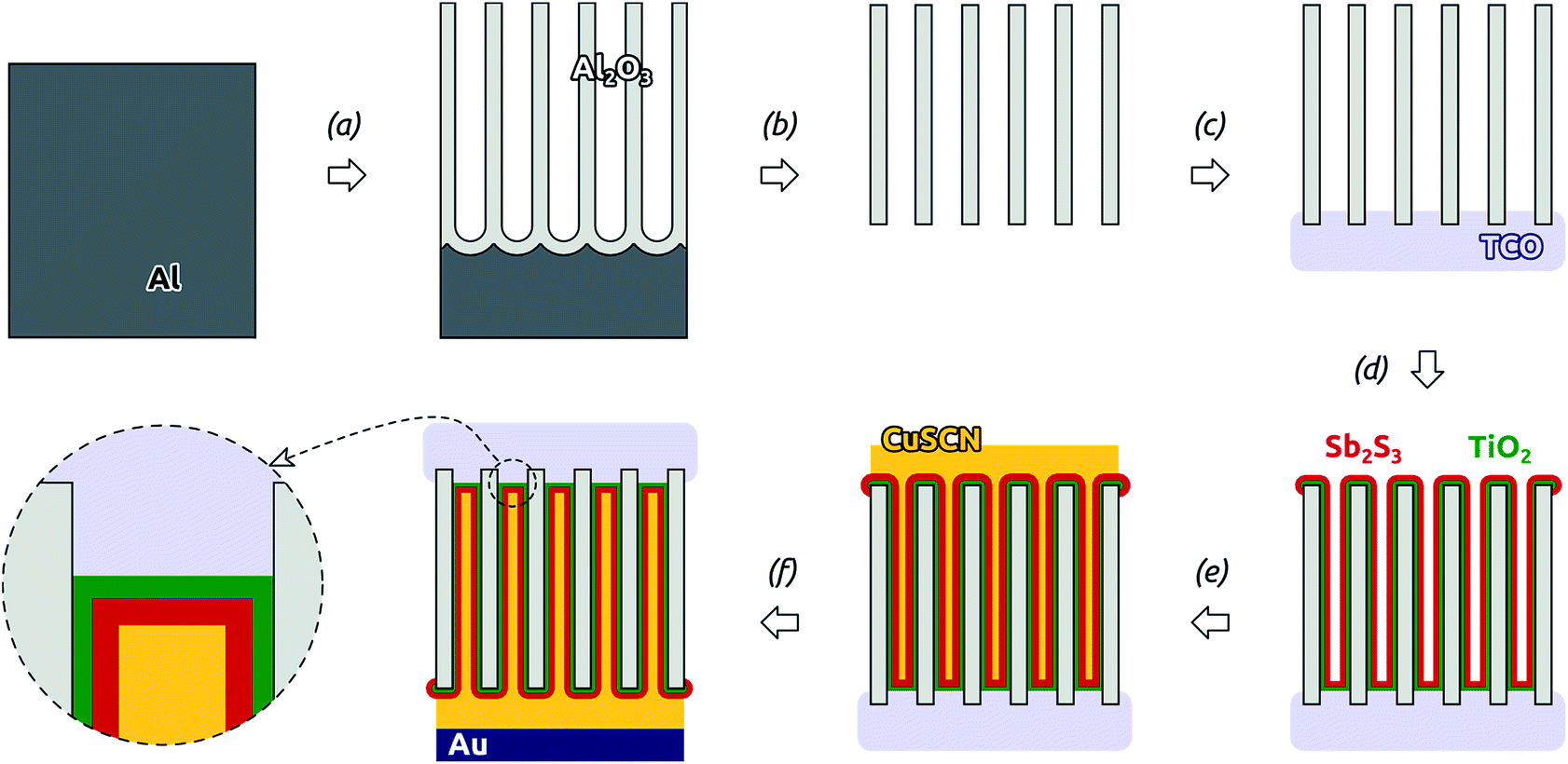 | ||
| Scheme 2 Preparation of ‘extremely thin absorber’ (ETA) solar cells in ordered arrays of coaxial, nanocylindrical p-i-n junctions: (a) two-step anodization of Al, (b) wet chemical removal of the Al substrate (Cu2+) and the Al2O3 barrier layer, pore widening (H+), (c) RF sputter coating of the transparent conducting oxide (TCO), (d) ALD of TiO2 and Sb2S3, (e) evaporative infiltration of CuSCN, (f) Au DC sputter coating. | ||
With long durations of the exposure and purge within each ALD cycle (exposure 50 s, purge 60 s) performed at 120 °C in our home-built hot-wall reactor, the ALD reaction26 between Sb(NMe2)3 and H2S delivers reproducible Sb2S3 coatings in cylindrical, straight pores of 80 nm diameter and 30 μm length. Fig. 1(a) displays a scanning electron micrograph (SEM) of a sample in which pores closed at one extremity with the barrier layer of oxide were coated with TiO2 and Sb2S3 consecutively, after which the barrier layer was removed in acid. On the side of the sample which used to be closed by the barrier layer (the deepest point of the pores for ALD precursor diffusion), the hemispherical closed extremities of the acid-resistant TiO2 tubes visibly protrude out of the matrix. The energy-dispersive X-ray spectrum (EDX) taken on the same sample area, presented in Fig. 1(b) and quantified in Table 1, exhibits exclusively the elements expected for Al2O3, TiO2 and Sb2S3. Most importantly, the elements constituting Sb2S3 are detected by EDX in significant amounts, even though the method only probes the uppermost micron of the sample. This demonstrates the penetration of Sb2S3 ALD into the 30 μm long pores. Additionally, the 2![[thin space (1/6-em)]](https://www.rsc.org/images/entities/char_2009.gif) :3 stoichiometric ratio of the compound is reflected in the EDX intensities obtained for Sb and S, within uncertainty. Note that the elemental EDX composition discussed here is representative of other positions of the sample, including its cross-section and its front side.
:3 stoichiometric ratio of the compound is reflected in the EDX intensities obtained for Sb and S, within uncertainty. Note that the elemental EDX composition discussed here is representative of other positions of the sample, including its cross-section and its front side.
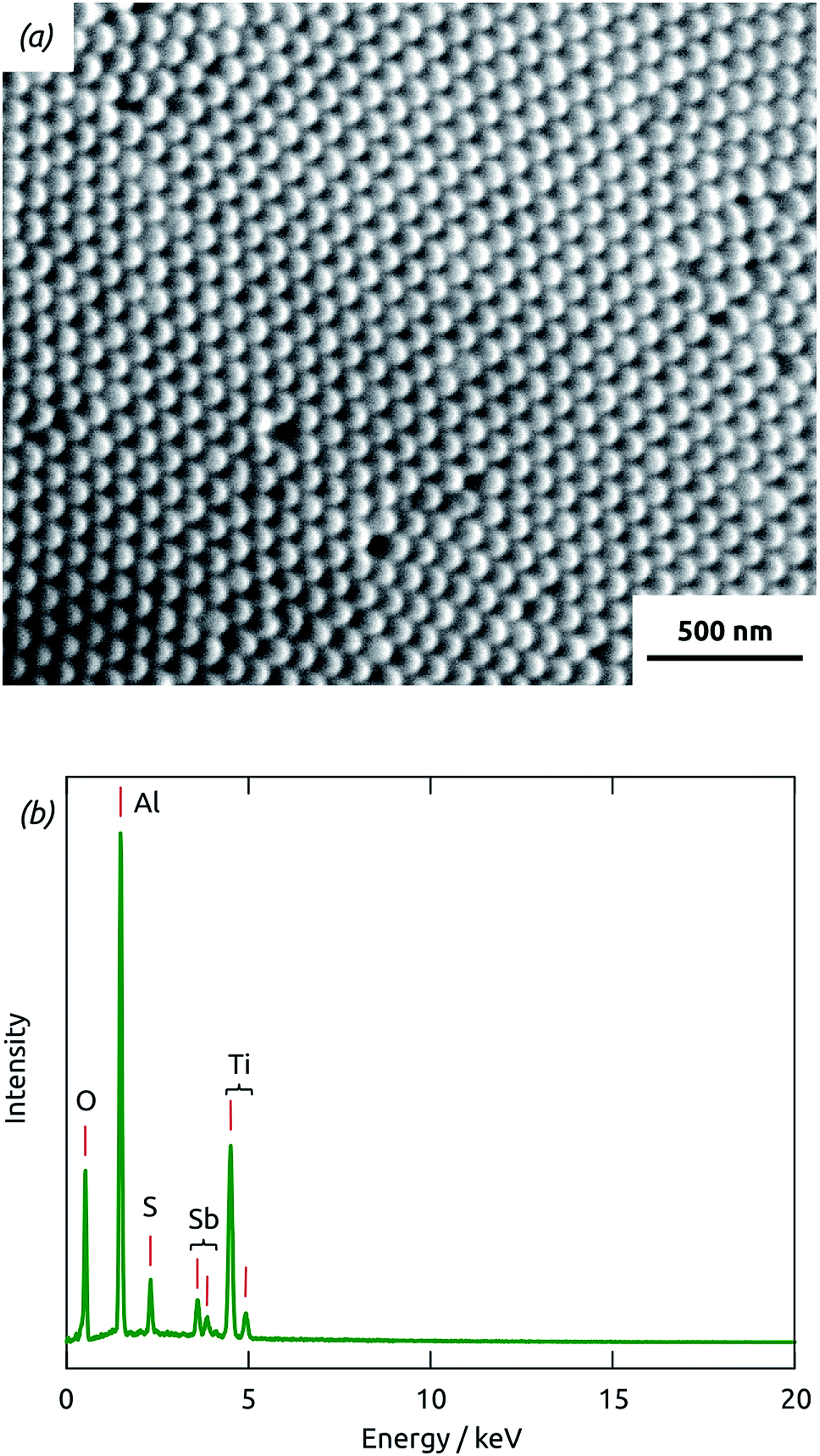 | ||
| Fig. 1 (a) Scanning electron micrograph of the backside of a sample coated with TiO2 and Sb2S3 ALD after the barrier layer of alumina closing the pore extremities was removed. (b) Energy-dispersive X-ray (EDX) spectrum recorded on the area displayed in (a), together with the corresponding element labels. | ||
| Element | Line | Atomic composition |
|---|---|---|
| O | Kα | 67.3% |
| Al | Kα | 20.2% |
| S | Kα | 1.9% |
| Ti | Kα | 9.2% |
| Sb | Lα | 1.4% |
The maximal ALD deposition depth achievable in our cylindrical pores can be determined by EDX profiles along the depth axis of thick matrices. Fig. 2 displays results obtained with two membranes of 20 μm (a) and 50 μm (b), respectively. Note that for this study, care was taken to leave the barrier layer of oxide closing one pore extremity intact, so that penetration of ALD precursor gases into the pores is unidirectional. In both cases, the pore opening is presented on the left-hand side of the graph (near distance zero). The short pores are obviously coated completely with an Sb2S3 layer of homogeneous composition, whereby a slight but significant downwards trend of the Sb2S3 amount is observable from the pore opening to the extremity (about 30% over 20 μm). Such a variation, albeit undesirable, is within the range tolerable for applications. It certainly represents a large improvement over solution-based deposition methods (‘chemical bath deposition’ or CBD), traditionally used for ETA cells.30–32 The sample with the longer pores demonstrates the limit reachable by our ALD method (with the conditions used in this study). The first 20 μm of the pores are coated essentially homogeneously, whereas the Sb2S3 amount (corresponding to the thickness of the deposited layer) drops to zero between the thicknesses 20 μm and 35 μm. Thus, our ALD method is limited to straight pores of aspect ratio 1:250 if conformal coatings are essential, and can be applied up to aspect ratio 1:370 or so if a strong thickness variation can be tolerated for the application. It should be possible to increase the deposition depth further by increasing the precursor dosage (via exposure duration and/or precursor bottle temperature), and possibly by varying the reaction chamber temperature, as well.
 | ||
| Fig. 2 Energy-dispersive X-ray spectroscopic profiles of samples prepared by Sb2S3 ALD in porous alumina templates, observed in cross-section. The samples have overall thicknesses of (a) approx. 20 μm and (b) approx. 50 μm. Gray, Al; red, S; orange, Sb; blue, Au; brown, Cu. The elements C and O are not accounted for in the percentage values. The data points corresponding to analyses outside the confines of the sample (where percentages are not meaningful) are grayed out for clarity. A 5 nm Au layer was sputtered for investigation for better conductivity, and the Cu signal is an artefact originating from the sample holder. | ||
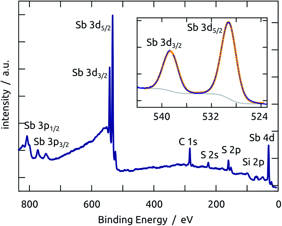
X-ray photoelectron spectroscopy performed on a planar Sb2S3/SiO2/Si sample demonstrates that not only the bulk of the material deposited is stoichiometric and free of oxide, but also its surface. The spectrum presented in Fig. 3 is dominated by the prominent Sb 3d peaks in the region 520–540 eV.33 The other elements found are S (as expected) and C (due to the usual surface contamination). Silicon is practically absent, which demonstrates that the Sb2S3 layer is continuous and closed. The 1s peak of oxygen would be found near 528 eV, which would overlap with the Sb 3d signal. However, the experimental data can be perfectly fitted with only the Sb doublet (the spin–orbit splitting is 9.6 eV and the maxima are located at 529.6 and 539.2 eV respectively, consistent with previous studies),34–36 without any O contribution, as shown in the inset of Fig. 3.
 | ||
| Fig. 3 XPS spectrum recorded on an Sb2S3 layer grown on a Si/SiO2 wafer. The inset shows the high-resolution Sb 3d region: experimental data are drawn in deep blue, the Shirley background in gray and the calculated fit (with two Gaussian peaks) in orange. | ||
Annealing the initially amorphous Sb2S3 layers deposited by ALD not only causes crystallization, it may also affect the morphology of the films. Fig. 4 compares transmission electron micrographs of Sb2S3 films grown on flat Si(100) wafers covered by a 200 nm thick thermal SiO2 layer (a) before and (b) after an annealing post-treatment carried out at 315 °C for 5 hours in Ar atmosphere. As grown, the Sb2S3 solid film is a smooth and continuous layer exhibiting a thickness of about 20 nm after 500 ALD cycles. Upon annealing, the film dewets and contracts to large crystallites of 50 to 200 nm diameter on the SiO2 layer. This phenomenon shows the potentially significant mobility of the solid at elevated temperature,29,37 as well as its poor adhesion to certain oxidic surfaces.38
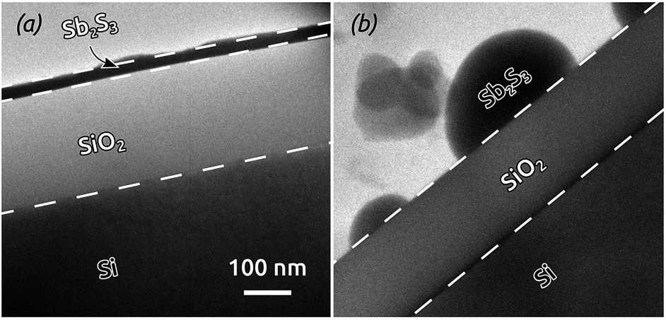 | ||
| Fig. 4 TEM micrographs showing the cross-section of an Sb2S3 layer deposited on thermal silicon oxide, (a) as grown and (b) after subsequent annealing at 315 °C. Both micrographs are presented at the same scale. | ||
However, the planar Si/SiO2 substrate, although convenient for TEM investigation, is not representative of our photovoltaic samples, in which the Sb2S3 layer not only experiences a different underlying oxide, but also a certain geometric confinement. Realistic data were collected on nanoporous samples by in situ XRD monitoring during annealing. Fig. 5 summarizes all data collected on a nanoporous sample in which amorphous Sb2S3 was coated onto crystalline TiO2, and evidences that crystallization starts slightly below 300 °C already. It is also found to be highly dependent on the exact geometry, chemical identity, and crystal structure of the surface. To characterize these effects, the behavior of various Sb2S3 layer thicknesses on three different substrates are compared in Fig. 6: (1) Sb2S3 on bare (amorphous) anodic alumina pores, (2) Sb2S3 on pores preliminarily coated by amorphous TiO2 (by ALD), and finally, (3) Sb2S3 on pores preliminarily coated by TiO2 and crystallized at 400 °C.
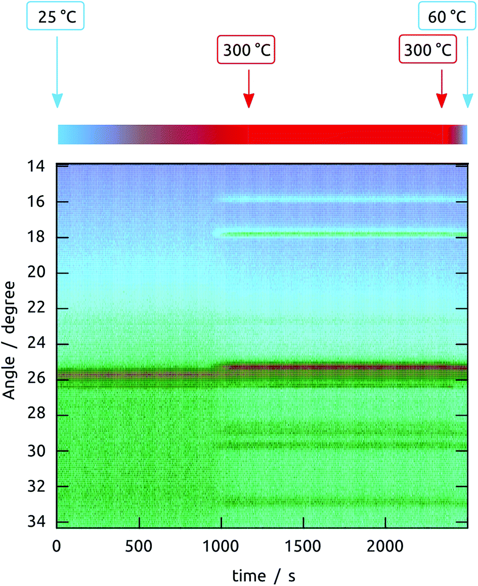 | ||
| Fig. 5 Full dataset obtained by in situ XRD monitoring of a sample upon annealing to 300 °C. The temperature is ramped up linearly from 25 °C to 300 °C, then maintained at 300 °C and finally cooled as sketched above the graph. The sample was prepared by anodization (pore diameter 80 nm, length >100 μm), followed by ALD of TiO2 (20 nm), crystallization of TiO2 (400 °C, 4 h), and finally ALD of Sb2S3 (10 nm). Color code: the X-ray signal intensity increases from blue to green to brown. The constant signal observed near 26° present from the very start is due to the initially crystalline TiO2. | ||
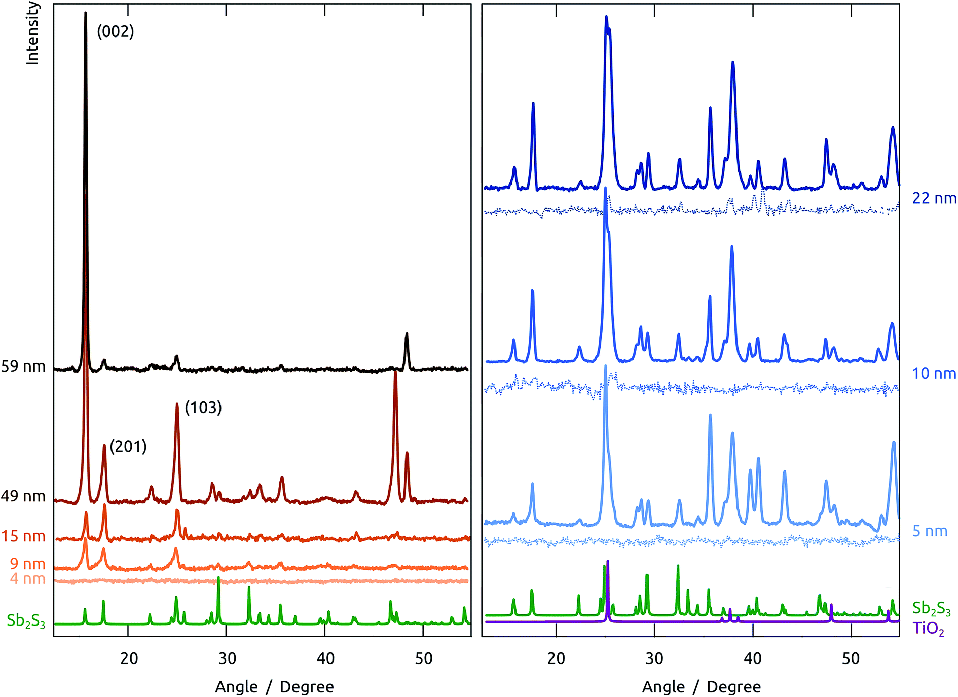 | ||
| Fig. 6 Contrasting crystallization behaviors of Sb2S3 layers of various thicknesses and on various substrates upon annealing to 300 °C in situ. Left, five different thicknesses in anodized alumina matrix. Right, three different thicknesses in the same matrix preliminarily coated with TiO2 (ALD, 20 nm); the solid lines represent samples the TiO2 layer of which was crystallized by annealing before the Sb2S3 ALD, the thin dotted lines refer to samples in which this annealing was not performed before Sb2S3 ALD. Reference spectra are provided for Sb2S3 in green,39 and for anatase TiO2 in purple.40 | ||
On the amorphous anodic alumina matrix, thin Sb2S3 layers (5 nm) do not crystallize at 300 °C (note that this is not due to the low absolute signal intensity, as we have demonstrated separately). Not only does crystallization occur only with at least 9 nm Sb2S3, but the crystallization behavior of thicker layers changes with thickness drastically. As long as the layer are thin with respect to the pore diameter (100 nm in this case), the low-index peaks (002), (201) and (103) appear in roughly powder intensity ratios. When the pore is completely filled with Sb2S3 (sample with nominal 59 nm thickness), crystallization takes place in a strongly preferred orientation, namely with the c axis parallel to the pore long axis. The situation is different altogether on amorphous TiO2. Here, no significant crystallization is evident. The case of crystalline TiO2 as the underlying surface yields yet another completely new picture. Indeed, all thicknesses of Sb2S3 crystallize on it with random orientation, as shown by the peak intensities, which follow the powder pattern over the full 2θ scale. This piece of information is encouraging for the final solar cell devices, as it allows one to expect not only a high crystal quality of the ‘extremely thin’ absorber layer, but also indicates a good interfacial contact between the individual semiconductors.
The capability of our methods to generate sample series in which one geometric parameter (either cylinder length L or wall thickness d) is varied systematically whereas the others are kept constant, and the value of this experimental possibility, is exemplified by the optical properties shown in Fig. 7. We note that the cylinder outer diameter D can also be experimentally varied, however at one given period of the order in the pore array, one expects a monotonous improvement of all performance parameters with D. In this paper, we therefore use a value of D close to the experimentally reachable maximum. All samples absorb essentially all photons more energetic than 500 nm, and transmit essentially all photons beyond 800 nm. That the experimental spectra rarely reach exactly A = 1 and A = 0 in these spectral regions is a common artifact of diffuse absorbance spectra, obtained by subtracting diffuse transmittance and diffuse reflectance from unity, due to ambiguities in referencing. Thus, the significant differences between the various samples are found in the band gap region, where A transitions form unity to zero.
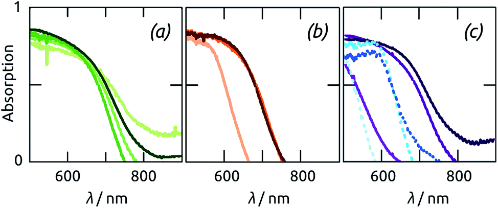 | ||
| Fig. 7 Optical properties (diffuse absorption A obtained from diffuse transmission and diffuse reflection) of nanotubular Sb2S3 samples with various geometric parameters (length L and tube wall thickness d). (a) Variation of L at constant d = 9.5(±0.5) nm: L = 10/20/30/50 μm (±10%), from light green to dark green. (b) Variation of d at constant L = 30(±3) μm: d = 6/10/13(±0.5) nm, from orange to brown. (c) Effect of annealing at constant L = 35(±3) μm: the wall thicknesses d = 6/10/15(±0.5) nm are represented in increasingly dark shades of dashed blue before annealing and of solid purple after it. | ||
The absorption range of Sb2S3 samples grown with the same ALD deposition in pores of different lengths increases with L, as expected (Fig. 7(a)). However, no further improvement is obtained beyond L = 30 μm, which corresponds to the limitation in ALD penetration depth described above. Light absorption is also increased by d (Fig. 7(b)). However, for the rather long samples studied here, increases beyond 10 nm do not result in any measurable gain. The structural changes occurring upon annealing (documented above) are also apparent in the optical properties of the samples (Fig. 7(c)). The absorption band edge shifts by almost 100 nm (from somewhat beyond 650 nm to almost 750 nm) for the sufficiently thick Sb2S3 layers, which crystallize efficiently. In contrast to this, the variation is minute for the 5 nm thick sample, due to its unsuccessful or incomplete crystallization demonstrated by XRD.
Physical characterization of films, junctions, and functional solar cells
Once a sample is prepared through all steps of Scheme 1, a functional solar cell is obtained, as demonstrated by the I–V curves of Fig. 8 in the dark and under irradiation (1 sun). The curves measured following preparation immediately are not completely stable: the samples must be first stabilized by passing moderate current for a couple of hours before the properties are quantitatively reproducible. | ||
| Fig. 8 Electrical current–voltage curves recorded at 1 mV s−1 on a sample of 0.126 cm2 area with L = 30 μm, d(TiO2) = d(Sb2S3) = 11 nm: blue and red, dark and irradiated curves recorded on a freshly prepared sample; green and orange, dark and irradiated curves recorded after several hours of electrical measurements. Solar spectrum AM1.5 irradiation was performed under 1 sun. | ||
A slightly hysteretic behavior is often observed on the I–V curves, as in Fig. 8. The timescales associated with it are characterized by time-resolved measurements of open-circuit potential and short-circuit current, shown in Fig. 9. The UOC and ISC buildups upon exposure to solar light are essentially instantaneous (<100 ms), indicating that our materials have few traps that can be occupied by photogenerated carriers. The UOC(t) decay obtained after turning off the irradiation is monoexponential and characterized by a lifetime of 117(±2) ms. This corresponds to a recombination lifetime of the photogenerated charge carriers in our experimental conditions, and is in line with values reported for photovoltaic systems based on TiO2 nanocrystals of colloidal origin.41–43 In addition to this, both UOC and ISC also decay from their respective value obtained immediately after turn-on, with contrasting lifetimes on the order of tens of seconds (for UOC) and hundreds of milliseconds (for ISC). This behavior has been described as an effective ‘negative capacitance’ and observed in this type of solar cell in numerous cases.44
 | ||
| Fig. 9 Time-dependent behavior of (a) open-circuit potential and (b) short-circuit current upon turning full-spectrum irradiation at 1 sun on (white) and off (gray). | ||
Further insight into the phenomena limiting the performance of our system, and more reliable values of the time constants involved, are provided by impedance spectroscopy. Fig. 10(a) shows data recorded at +0.1 V bias in the dark and under irradiation. The overall real resistance, evident as the abscissa of the lowest-frequency points (on the right-hand side), is reduced by over an order of magnitude upon irradiation, as should be the case. The evolution of the Nyquist plots from +0.1 V to −0.1 V under irradiation is shown in Fig. 10(b). The shape of all curves can be described as a significantly depressed semicircle. Consequently, an equivalent circuit model featuring three RC elements in series (in addition to the series resistance, Fig. 10(c)) must be used to deliver adequate fits (thin dashed black curves) to the experimental data.
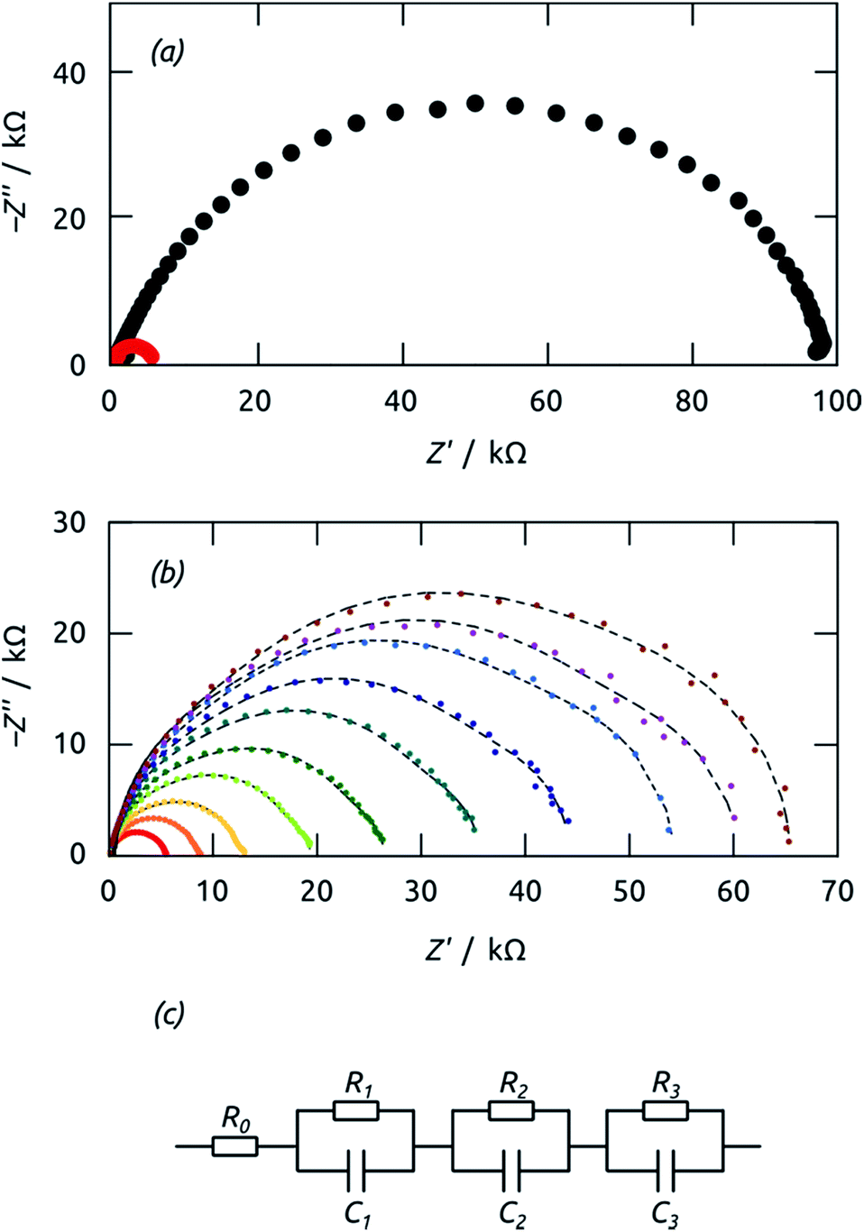 | ||
| Fig. 10 (a) Nyquist plots of impedance spectroscopy data recorded on a cell (area 0.126 cm2) in the dark (black) and under 1 sun irradiation (red) at +0.1 V. (b) Nyquist plots of the same cell recorded under 1 sun at various voltages from −0.1 V (brown datapoints) to +0.1 V (red datapoints). The dashed lines are curves calculated from a fit. (c) Equivalent circuit model used for fitting the data. | ||
The characteristic time constants obtained in short circuit conditions are τ1 = 13 ms, τ2 = 40 ms, and τ3 = 6 ms. The short constants are not accessible in the UOC(t) and ISC(t) experiments of Fig. 9, but we note that τ2 coincides with the decay time constants observed in the real-time curves rather well. The attribution of τ2 to recombination is corroborated by the very large capacitance value of C2 = 56 μF cm−2 (at 0 V), which is larger than C1 and C3 by factors larger than 50 and 20, respectively. Indeed, this large value must be expected based on the large specific surface area of our elongated nanocylindrical p-i-n junction. The corresponding resistance is R2 = 750 Ω cm2 (still at 0 V), which is comparable to values reported for a colloidal TiO2/Sb2S3/CuSCN system.45 We attribute the resistance R1 to the p-CuSCN phase based on its very limited, linear variation with applied potential (Fig. 11): the values are larger than those reported in the colloidal system,41 consistent with the longer transport paths to the electrode in our system (30 μm, as compared to ≤3 μm in the colloidal case). Finally, the remaining resistance R3 = 2.6 kΩ cm2 must be associated with transport in the n-TiO2 phase. The large value is likely related to the geometry (long TiO2 tubes with thin walls), and seems to be the major factor limiting the performance of our novel system.
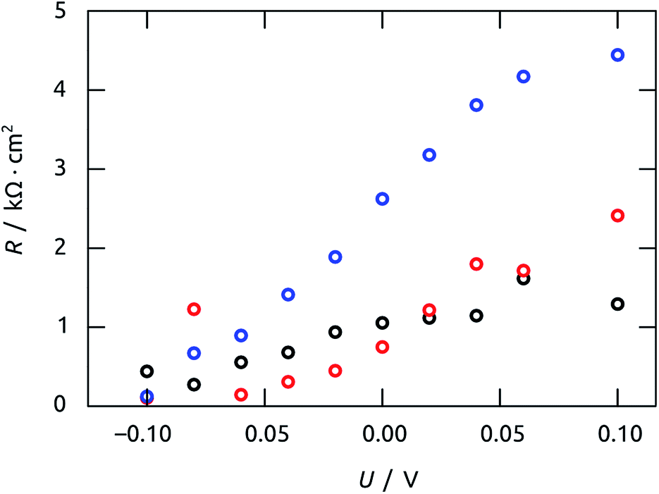 | ||
| Fig. 11 Values of resistances R obtained by impedance spectroscopy vs. applied potential U. The values were calculated from the model of Fig. 10(c) to fit the Nyquist plots in Fig. 10(b). Color code: R1, black; R2, red; R3, blue. | ||
Insight into exciton dynamics and charge transfer processes, which occur on much faster timescales, is obtained by femtosecond transient absorption spectroscopy of a crystalline, planar Sb2S3 film deposited on ITO, as a transparent layer able to accept both electrons and holes (since its Fermi energy lies higher than its conduction band edge).46,47 It has been established that holes, instead of electrons, limit the overall kinetics of charge separation in the materials system studied here, as the transport of localized holes within Sb2S3 and their subsequent transfer into another phase are slow.48,49 When excited with ultrashort (i.e. 150 fs) pump pulses at 665 nm and probed with temporally delayed, white-light continuum probe pulses, the sample gives rise to two salient features (Fig. 12). A photoinduced bleach due to exciton formation appears within 1 ps near 460 nm, whereas a transient absorption centered around 600 nm emerges later and can be attributed to the localized trapping of valence-band holes (likely at interfaces).48
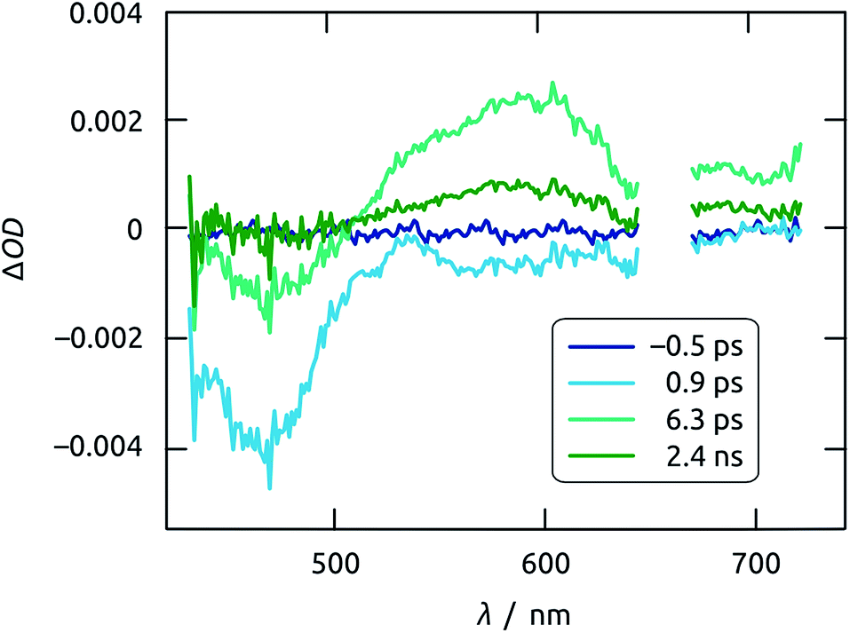 | ||
| Fig. 12 Time evolution of the transient absorption spectra of Sb2S3 film on ITO excited using 665 nm pump pulses. Note that the spectrum recorded at negative time is a perfect blank. | ||
The bleach at 460 nm recovers with monoexponential kinetics characterized by τb = 2 ps. This value is identical (within uncertainty) to the characteristic rise time of the transient absorption of trapped holes, recorded at 620 nm (Fig. 13(a)). Thus, either the photogenerated hole is captured very quickly and localized, or the exciton recombines nonradiatively on a somewhat slower time scale. The trapped holes disappear on a much slower timescale, with a decay time of τa = 1 ns (in addition to a minor component on the order of 10 ps), as shown in Fig. 13(b). The physical process taking place on the 1 ns timescale is unveiled by comparison with a Sb2S3 film sample grown directly on glass, that is, in which holes cannot be injected into a second semiconductor. In this reference sample, the transient absorption signal (recorded at 590 nm) also appears concurrently with the decay of the bleach, but remains constant at a non-zero, positive value on the nanosecond scale. That this trapped state is long-lived on glass but decays with τa = 1 ns on ITO assigns it as being due to hole injection into ITO. The timescale found in this system for hole injection coincides with that determined previously in a TiO2/Sb2S3/CuSCN cell in which Sb2S3 particles were generated by chemical bath deposition.48
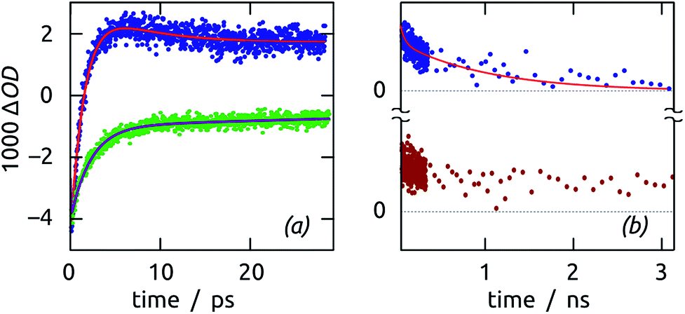 | ||
| Fig. 13 Dynamics of Sb2S3 thin film samples. (a) Ultrafast decay of the exciton bleach (460 nm, green) and subsequent appearance of a transient absorption due to trapped holes (620 nm, blue) in Sb2S3/ITO. (b) Slow decay of the trapped holes in the Sb2S3/ITO system (620 nm, blue), compared to the non-decaying signal recorded for Sb2S3/glass (590 nm, brown). | ||
This confirms the capability of our ALD-grown light absorber to carry out its function in ETA cells. Therefore, we can conclude that physical insight to be gained in the future from our model system featuring the well-defined nanocylindrical geometry will be applicable to understanding ETA systems generated by colloidal methods, as well.
Experimental
Materials
Oxalic acid, phosphoric acid, copper(II) chloride dihydrate, chromium(VI) oxide, ethanol, hydrochloric acid, perchloric acid, and argon were purchased from commercial suppliers and used as received. The ALD precursor tris(dimethylamido)antimony(III) was from Sigma Aldrich, H2S from Air Liquide (3% H2S in N2), and Ti(OiPr)4 from Alfa Aesar. The p-semiconductor CuSCN was obtained from Strem Chemical, iPr2S from Alfa Aesar and LiSCN from Sigma Aldrich. The aluminum (99.999%) for anodization was purchased from Goodfellow. Boron-doped [100] CZ silicon wafers with 200 nm thermal oxide were ordered from Silicon Materials. Water was purified immediately before use in a Millipore Direct-Q system. The sputter targets (ITO and Au) were obtained from Stanford Advanced Materials.Sample preparation
Characterization methods
Spectroscopic ellipsometry data were collected from 400 to 1000 nm under a 70° incidence angle with an instrument model EL X-02 P Spec from DRE Dr Riss Ellipsometerbau GmbH. Fits were performed using the database of material files provided with the instrument or the optical spectra published for amorphous Sb2S3.26Diffuse optical absorption spectroscopy was measured using a DH-2000-L light source, an HR4000 spectrometer, and an ISP-50-8-R integrating sphere from OceanOptics. For each sample, a diffuse transmission spectrum was recorded with respect to a blank taken without sample, and then a diffuse reflectance spectrum was recorded with respect to a blank taken on a reflective standard (anodic alumina membrane with underlying aluminum substrate). The diffuse absorption (A) spectra displayed in the article were obtained by subtracting the transmitted and reflected/scattered intensities (T and R, respectively) from the incident intensity, A = 1 − T − R.
Scanning electron micrographs were taken on a Jeol JSM 6400 equipped with a LaB6 cathode and with an EDX system based on an SDD detector. Transmission electron microscopy (TEM) of ion-milled thin sample sections was performed on a Jeol 3010 equipped with a LaB6 cathode.
The electrochemistry data were collected with a CompactStat potentiostat from Ivium Technologies and the impedance spectroscopy fits were performed between 17782.8 Hz and 1 Hz by the instrument's software. A solar simulator from Newport Model 69907 with a 150 W Xe lamp was used as the light source and the light intensity was calibrated to AM1.5 with a reference Si solar cell.
The chemical surface composition analysis was performed by X-ray photoelectron spectroscopy (XPS) using a Mg Kα (1253.6 eV) source from a commercial HA 150 VSW spectrometer, on a planar sample prepared by depositing approximately 20 nm of Sb2S3 onto a Si wafer. The energy scale was calibrated on the C 1s peak. Spectrum fitting was performed with the XPS Peak 4.1 software, whereby a Shirley background was used. An identical sample was investigated by TEM after preparation of a microtome lamella.
Annealing of the Sb2S3 layers with in situ X-ray diffraction (XRD) monitoring was performed in an experimental stainless steel heating chamber, mounted in a dedicated Bruker D8 Discover. Cu K-alpha radiation (λ = 0.15406 nm) was used as the X-ray source, while a linear Vantec detector monitored the crystallinity of the thin films. The samples were heated in a helium atmosphere to 300 °C at a rate of 0.25 °C s−1, after which the temperature was kept constant for 30 min. The diffraction pattern was captured over a 2θ range of 20° in 4 s intervals.
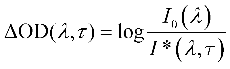
Femtosecond transient absorption spectroscopy experiments were conducted on planar samples (8.5 nm Sb2S3 on glass and 30 nm Sb2S3 on ITO/glass) with a Clark MXR CPA 2101 laser system in conjunction with an Ultrafast TAPPS HELIOS detection system, consisting primarily of a glass fiber based spectrometer. Output pulses at 387 nm and 665 nm with a 150 fs pulse and a 1 kHz repetition rate were used as pump pulses. They were obtained by amplifying and frequency-doubling the 775 nm seeding pulses of the Er3+-doped glass fiber oscillator in a regenerative chirped-pulse titanium-sapphire amplifier and with either a frequency-doubling BBO crystal or a nonlinear optical parametric amplifier (NOPA). All samples were pumped at excitation energy densities per pulse between 100 and 300 μJ cm−2. A fraction of the fundamental was simultaneously passed through a sapphire plate (16 mm) to generate a fs white-light continuum between 400 and 1650 nm. Transient absorption spectra were taken at delay times between −2 ps and +1 ns. They were recorded between 450 and 730 nm in the magic-angle configuration of the polarization vectors of pump and probe pulse. The chirp of this spectral range was approximately 350 fs. No photochemical degradation was observed after each experiment, as the subsequently recorded absorption spectra of the samples showed. The transient absorption spectra were obtained as temporal evolution of the spectral changes in the optical density (ΔOD) of the sample. Therefore a chopper wheel provided the blocking of every other pump pulse so that the probe pulse was alternately transmitted through a pump-pulse excited and a ground-state sample. The intensity of the transmitted probe pulse after the pump pulse excited sample, I*(λ, τ), and that without pump pulse excitation, I0(λ) were measured as function of the delay time τ. The ΔOD values were determined as
For I0(λ) > I*(λ, τ) the ΔOD signal attains positive values and is assigned to absorption transitions of excited species, the so-called photoinduced absorption (PIA), whereas negative values of ΔOD result from I0(λ) < I*(λ, τ) and are ascribed to photoinduced bleaching (PIB) of the ground state population density. Single-wavelength kinetic traces were fitted with exponentials or biexponentials after deconvolution of the apparatus time response function.
Conclusions
An ALD-based method for generating parallel arrays of elongated, cylindrical p-CuSCN/i-Sb2S3/n-TiO2 coaxial heterojunctions is established and yields functional ETA solar cells. The cylinders are arranged hexagonally with a 105 nm pitch, they have a fixed outer diameter of 80 nm and a length L tunable up to a maximal 30 μm. The hole conductor and light absorber layers thicknesses d can be set accurately between 0 and 20 nm approximately. The crystallization behavior and optical properties of Sb2S3 depend strongly on the geometric parameters L and d(Sb2S3), as well as on the identity of the underlying surface. The transfer of photogenerated holes out of the light-absorbing layer occurs on the timescale of 1 ns, as is the case in similar materials systems prepared with colloidal methods. In the sample geometry presented in this paper, characteristic lifetimes associated with transport and recombination are on the millisecond timescale. Recombination of charge carriers at the large interface areas is the likely cause of the low power conversion efficiency recorded here. Thus, reducing the charge carrier transport distances by shortening the cylinder length L will likely improve the device performance.This piece of work provides the long-sought preparative scheme towards ordered nanorod solar cells. Our scheme is quite practical experimentally and highly general. Members of the photovoltaics community can now apply it to the generation of series of samples in which each geometric parameter (rod diameter and length, individual layer thicknesses) is varied systematically. They can also replace each of the three materials with alternatives, given that many n-type oxides are accessible by ALD, as well as several intrinsic semiconductor compounds of the heavier chalcogens featuring large extinction coefficients.
Acknowledgements
Our work was supported by the DFG Excellence Cluster ‘Engineering of Advanced Materials’ and by the Centre de Coopération Universitaire Franco-Bavarois/Französisch-Bayrisches Hochschulzentrum (CCUFB/FBHZ). The in situ XRD measurements were supported by Flanders (FWO), UGENT-GOA-01G01513 and IWT-SBO. The fs TA measurements were supported by the Deutsche Forschungsgemeinschaft (graduate school 1161/2). We thank M. Künzel (FAU) for his support with optical absorption measurements, as well as D. Chaudanson, S. Nitsche and J.-Y. Hoarau (CINaM) for TEM observations and XPS measurements.References
- K. M. Coakley and M. D. McGehee, Chem. Mater., 2004, 16, 4533 CrossRef CAS.
- G. Dennler and N. S. Sariciftci, Proc. IEEE, 2005, 93, 1429 CrossRef CAS.
- A. Hagfeldt and M. Grätzel, Acc. Chem. Res., 2000, 33, 269 CrossRef CAS.
- M. Grätzel, Chem. Lett., 2005, 34, 8 CrossRef.
- C. Groves, O. G. Reid and D. S. Ginger, Acc. Chem. Res., 2010, 43, 612 CrossRef CAS PubMed.
- R. A. Marsh, C. R. McNeill, A. Abrusci, A. R. Campbell and R. H. Friend, Nano Lett., 2008, 8, 1393 CrossRef CAS PubMed.
- N. Tigau, V. Ciupina, G. I. Rusu, G. Prodan and E. Vasile, Rom. J. Phys., 2005, 50, 859 CAS.
- P. Pattanasattayavong, N. Yaacobi-Gross, K. Zhao, G. O. Ngongang Ndjawa, J. Li, F. Yan, B. C. O'Regan, A. Amassian and T. D. Anthopoulos, Adv. Mater., 2013, 25, 1504 CrossRef CAS PubMed.
- B. C. O'Regan and F. Lenzmann, J. Phys. Chem. B, 2004, 108, 4342 CrossRef.
- Y. Xu and M. A. A. Schoonen, Am. Mineral., 2000, 85, 543 CrossRef CAS.
- W. H. Strehlow and E. L. Cook, J. Phys. Chem. Ref. Data, 1973, 2, 163 CrossRef CAS.
- M. Grätzel and F. P. Rotzinger, Chem. Phys. Lett., 1985, 118, 474 CrossRef.
- K. Hara, H. Sugihara, L. P. Singh, A. Islam, R. Katoh, M. Yanagida, K. Sayama, S. Murata and H. Arakawa, J. Photochem. Photobiol., A, 2001, 145, 117 CrossRef CAS.
- C. A. Melendres, T. J. O'Leary and J. Solis, Electrochim. Acta, 1991, 36, 505 CrossRef CAS.
- B. M. Kayes, H. A. Atwater and N. S. Lewis, J. Appl. Phys., 2005, 97, 114302 CrossRef.
- K. Tennakone, G. R. R. A. Kumara, I. R. M. Kottegoda, V. P. S. Perera and G. M. L. P. Aponsu, J. Phys. D: Appl. Phys., 1998, 31, 2326 CrossRef CAS.
- I. Kaiser, K. Ernst, C.-H. Fischer, R. Könenkamp, C. Rost, I. Sieber and M. C. Lux-Steiner, Sol. Energy Mater. Sol. Cells, 2001, 67, 89 CrossRef CAS.
- R. L. Puurunen, J. Appl. Phys., 2005, 97, 121301 CrossRef.
- J. Bachmann, J. Jing, M. Knez, S. Barth, H. Shen, S. Mathur, U. Gösele and K. Nielsch, J. Am. Chem. Soc., 2007, 129, 9554 CrossRef CAS PubMed.
- J. Bachmann, R. Zierold, Y. T. Chong, R. Hauert, C. Sturm, R. Schmidt-Grund, B. Rheinlnder, M. Grundmann, U. Gösele and K. Nielsch, Angew. Chem., Int. Ed., 2008, 47, 6177 CrossRef CAS PubMed.
- Y. T. Chong, D. Görlitz, S. Martens, M. Y. E. Yau, S. Allende, J. Bachmann and K. Nielsch, Adv. Mater., 2010, 22, 2435 CrossRef CAS PubMed.
- H. Wedemeyer, J. Michels, R. Chmielowski, S. Bourdais, T. Muto, M. Sugiura, G. Dennler and J. Bachmann, Energy Environ. Sci., 2013, 6, 67 CAS.
- O. Jessensky, F. Müller and U. Gösele, Appl. Phys. Lett., 1998, 72, 1173 CrossRef CAS.
- J. Bachmann, Beilstein J. Nanotechnol., 2014, 5, 245 CrossRef PubMed.
- A. B. F. Martinson, M. S. Góes, F. Fabregat-Santiago, J. Bisquert, M. J. Pellin and J. T. Hupp, J. Phys. Chem. A, 2009, 113, 4015 CrossRef CAS PubMed.
- R. B. Yang, J. Bachmann, M. Reiche, J. W. Gerlach, U. Gösele and K. Nielsch, Chem. Mater., 2009, 21, 2586 CrossRef CAS.
- R. B. Yang, J. Bachmann, E. Pippel, A. Berger, J. Woltersdorf, U. Gösele and K. Nielsch, Adv. Mater., 2009, 21, 3170 CrossRef CAS.
- D. H. Kim, S. J. Lee, M. S. Park, J. K. Kang, J. H. Heo, S. H. Im and S. J. Sung, Nanoscale, 2014, 6, 14549 RSC.
- R. B. Yang, N. Zakharov, O. Moutanabbir, K. Scheerschmidt, L. M. Wu, U. Gösele, J. Bachmann and K. Nielsch, J. Am. Chem. Soc., 2010, 132, 7592 CrossRef CAS PubMed.
- D. S. Boyle, P. O'Brien, D. J. Otway and O. Robbe, J. Mater. Chem., 1999, 9, 725 RSC.
- P. P. Hankare, V. M. Bhuse, K. M. Garadkar, S. D. Delekar and I. S. Mulla, Semicond. Sci. Technol., 2004, 19, 70 CrossRef CAS.
- P. O'Brien and J. McAleese, J. Mater. Chem., 1998, 8, 2309 RSC.
- V. P. Zakaznova-Herzog, S. L. Harmer, H. W. Nesbitt, G. M. Bancroft, R. Flemming and A. R. Pratt, Surf. Sci., 2006, 600, 348 CrossRef CAS.
- C. M. Park, Y. Hwa, N. E. Sung and H. J. Sohn, J. Mater. Chem., 2010, 20, 1097 RSC.
- http://srdata.nist.gov/xps/ .
- Handbook of X-ray photoelectron spectroscopy, ed. C. D. Wagner, W. M. Riggs, L. E. Davis, J. F. Moulder and G. E. Muilenberg, Perkin-Elmer Corporation, Physical Electronics Division, 1979 Search PubMed.
- C. V. Thompson, Annu. Rev. Mater. Res., 2012, 42, 399 CrossRef CAS.
- P. R. Gadkari, A. P. Warrant, R. M. Todi, R. V. Petrova and K. R. Coffey, J. Vac. Sci. Technol., A, 2005, 23, 1152 CAS.
- ICSD_171568.
- ICSD_9853.
- Z.-S. Wang, M. Yanagida, K. Sayama and H. Sugihara, Chem. Mater., 2006, 18, 2912 CrossRef CAS.
- K. Zhu, N. R. Neale, A. Miedaner and A. J. Frank, Nano Lett., 2007, 7, 69 CrossRef CAS PubMed.
- M. Quintana, T. Edvinsson, A. Hagfeldt and G. Boschloo, J. Phys. Chem. C, 2007, 111, 1035 CAS.
- I. Mora-Sero, J. Bisquert, F. Fabregat-Santiago, G. Garcia-Belmonte, G. Zoppi, K. Durose, Y. Proskuryakov, I. Oja, A. Belaidi, T. Dittrich, R. Tena-Zaera, A. Katty, C. Levy-Clément, V. Barrioz and S. J. C. Irvine, Nano Lett., 2006, 6, 640 CrossRef CAS PubMed.
- P. P. Boix, G. Larramona, A. Jacob, B. Delatouche, I. Mora-Seró and J. Bisquert, J. Phys. Chem. C, 2012, 116, 1579 CAS.
- O. Malik and F. J. De la Hidalga-W, Physical and Technological Aspects of Solar Cells Based on Metal Oxide-Silicon Contacts with Induced Surface Inversion Layer, 2013, ch. 5, p. 124 Search PubMed.
- O. Malik, V. Grimalsky and J. De la Hidalga-W, J. Non-Cryst. Solids, 2006, 352, 1461 CrossRef CAS.
- J. A. Christians, D. T. Leighton and P. V. Kamat, Energy Environ. Sci., 2014, 7, 1148 CAS.
- J. A. Christians and P. V. Kamat, ACS Nano, 2013, 7, 7967 CrossRef CAS PubMed.
- T. Grünzel, Y. J. Lee, K. Kuepper and J. Bachmann, Beilstein J. Nanotechnol., 2013, 4, 655 CrossRef PubMed.
- Caution! Hydrogen sulfide is a highly toxic gas and should be used only in an appropriate environment, safety precautions include a fume hood, an alarm sensor, corrosion-resistant parts, and an exhaust H2S remover, we use Sulfatreat Select HP granules from MI Swaco on the exhaust line and a four-stage, eight-cylinder teflon-coated membrane pump MV10C from Vacuubrand.
| This journal is © The Royal Society of Chemistry 2015 |