
ITO-free highly bendable and efficient organic solar cells with Ag nanomesh/ZnO hybrid electrodes†
Myungkwan
Song‡
a,
Han-Jung
Kim‡
b,
Chang Su
Kim
a,
Jun-Ho
Jeong
b,
Changsoon
Cho
c,
Jung-Yong
Lee
c,
Sung-Ho
Jin
d,
Dae-Geun
Choi
*b and
Dong-Ho
Kim
*a
aAdvanced Functional Thin Films Department, Korea Institute of Materials Science, Changwon, 641-831, Republic of Korea. E-mail: dhkim2@kims.re.kr; Fax: +82-55-280-3570
bNano-Mechanical Systems Research Division, Korea Institute of Machinery & Materials (KIMM), 171 Jang-dong, Yuseong-gu, Daejeon, 305-343, Republic of Korea. E-mail: lamcdg@kimm.re.kr; Fax: +82-42-868-7123
cGraduate School of Energy, Environment, Water, and Sustainability (EEWS), Korea Advanced Institute of Science and Technology (KAIST), Daejeon, 305-701, Republic of Korea
dDepartment of Chemistry Education, Graduation Department of Chemical Materials, Institute for Plastic Information and Energy Materials, Pusan National University, Busan 609-735, Republic of Korea
First published on 3rd November 2014
Abstract
We demonstrate a facile approach to fabricate Ag nanomesh transparent conducting electrodes (TCEs) on a flexible substrate using nanoimprint lithography (NIL) and transfer printing without a conducting polymer. The Ag nanomesh TCEs exhibited a high transmittance of ∼88% and a low sheet resistance of ∼15 Ω sq−1 as well as superior mechanical flexibility. Furthermore, flexible inverted organic solar cells (IOSCs) with Ag nanomesh TCEs exhibited a power conversion efficiency (PCE) of ∼7.15% under 100 mW cm−2 AM 1.5G illumination as well as superior long-term stability under ambient conditions. This type of highly flexible and transparent Ag nanomesh electrode is a promising candidate for use with TCEs in various optoelectronic devices.
Organic solar cells (OSCs) have attracted significant interest because of their great potential to become a green energy source with a large-area, light-weight, mechanical flexibility, and low cost processes by roll-to-roll manufacturing.1–3 Recently, there have been extensive investigations of inverted organic solar cells (IOSCs) with an inverted structure, using modified indium tin oxide (ITO) as the cathode (the ITO is modified by an n-type metal oxide, a conjugated polyelectrolyte, and a self-assembled monolayer).4,5 Compared with conventional OSCs (COSCs), the IOSCs demonstrate better long-term air stability by avoiding the need for a corrosive and hygroscopic hole transport layer of poly(3,4-ethylenedioxythiophene):poly(styrenesulfonate) (PEDOT:PSS), and a low work function metal cathode, both of which are detrimental to the device lifetime.4,5 Furthermore, IOSCs can also offer vertical phase separation and concentration gradient in the photoactive layer, which is naturally self-encapsulated because air stable metals are used as the top electrode.6–9 Indium tin oxide (ITO), which is commonly used as a transparent conductive electrode (TCE), is not suitable as a transparent electrode for flexible devices because it is brittle and cracks easily under mechanical stress.8 Moreover, owing to the rapid depletion of elemental indium and the costs associated with the various vacuum deposition techniques used to produce ITO, its continued use is proving to be expensive. This, in turn, is significantly hindering the realization of low-cost and easy-to-fabricate flexible optoelectronic devices.
These key issues in the use of ITO are being addressed by the emergence of next-generation flexible transparent materials such as carbon nanotubes (CNTs),9–11 graphene,12–17 conducting PEDOT:PSS,18–22 silver nanowires (Ag NWs),23–28 and metal meshes.29–37 The performance of these materials for applications as TCEs is strongly affected by two parameters: optical transmittance and electrical conductivity. However, achieving high conductivity and high optical transmittance has been a challenge because these two properties are usually inversely proportional, and this often results in optoelectronic performance characteristics far inferior to those of the ITO.
Recently, CNTs have been extensively investigated for use as TCEs in OSCs.9,10 However, CNT-based TCEs typically exhibit high sheet resistance or high surface roughness due to a large tube-to-tube contact resistance, resulting in a deterioration in the performance of the OSCs. Moreover, Bae et al. demonstrated a roll-to-roll transfer of 30-inch graphene films with a low Rsheet of ∼30 Ω sq−1 at T550nm ≈ 90% using chemical vapor deposition.15 In contrast, solution-processed graphene films exhibited very poor electrical (Rsheet ≈ 300 Ω sq−1) and optical properties (T550nm ≈ 80%).12 In particular, Ag-NW films have emerged as one of the most promising substitutes for ITO, because they offer optical transmittance and electrical conductivity superior to their competitors.23–28 However, Ag-NW films still have issues with air stability and electrical contact, which makes them difficult for implementing in high-efficiency OSCs. The inherently rough surfaces of the Ag NWs produce a low shunt resistance, a high leakage current, and low device performance. In addition, the Ag-NW films are easily detached from the substrate due to a weak adhesive force.23,24 Recently, metal mesh electrodes have also attracted attention because of their superior optical/electrical properties, which can be easily tuned by changing the line width, spacing, and thickness of the metal pattern.29–35 In contrast to Ag-NW films, the work function of metal mesh electrodes for different applications can be easily controlled by changing the metallic materials.30,31,35
In recent years, uniform metal mesh electrodes with diameters less than 1 μm have been fabricated by nanoimprint lithography (NIL) or micro-transfer molding based on the conducting PEDOT:PSS polymer.36,37 In this case, a major drawback of the PEDOT:PSS polymer is its intrinsic acidity, which significantly deteriorates the performance of optoelectronic devices in terms of efficiency and lifetime. Recently, Krebs et al. proposed the fabrication of a metal micromesh pattern using a fast roll-to-roll printing method for ITO-free transparent conducting electrodes.38–40 The patterned metal mesh may be a promising candidate for high performance TCEs that would be applicable to the roll-to-roll processing of large-area flexible substrates.38–40 Although metal mesh electrodes already reportedly have good optical/electrical and mechanical properties, they have never been studied for their efficiency and stability when incorporated with OSCs using high-performance polymers prepared on a flexible substrate. Therefore, in this work, we demonstrate a method for preparing highly transparent, conductive, and bendable Ag nanomesh electrodes by NIL and transfer printing; this is accomplished without a conducting polymer and the resulting TCEs show promise for use in flexible OSCs. We found that Ag nanomesh electrodes exhibited a low Rsheet of ∼15 Ω sq−1 and a high optical transmittance of T550nm ≈ 88%. Moreover, the device performance of the inverted organic solar cells (IOSCs) incorporating these Ag nanomesh electrodes, which were fabricated on a flexible substrate, was found to be ∼97% of that of devices with ITO electrodes (the PCEs of the IOSCs using the Ag nanomesh electrodes and those using ITO electrodes were ∼7.15% and ∼7.35%, respectively).
Fig. 1(a) schematically illustrates our key process steps for producing highly conductive, transparent Ag nanomesh electrodes on a polyethersulfone (PES) film using a polyurethane acrylate (PUA) mold and a transfer printing method. Details for the fabrication conditions are described in the Experimental section of the ESI.†
 | ||
| Fig. 1 (a) Schematic of the fabrication procedures for transparent, conducting Ag nanomesh electrodes using a dry-transfer printing method. (b) SEM images of square-metal grids with a line width of 150 nm; a photograph of this metal mesh electrode on a PES substrate (10 × 10 cm). (c) Photographs of red LEDs connected to an Ag nanomesh electrode before and during bending. | ||
Fig. 1(b) and S1† show field emission scanning electron microscopy (FE-SEM) images of the Ag nanomesh electrode on PES and glass substrates, with a line width of 150 nm and line spacings of 1 μm, 1.6 μm, and 3.2 μm. It is obvious that all of the Ag nanomesh electrodes show a uniform square pattern. Moreover, the photograph shows high transparency as the symbol mark (KIMM) in the background can be clearly seen through the electrode. Furthermore, the electrode also exhibited excellent mechanical flexibility, as can be seen in Fig. 1(c), with illumination in the red LED lamp even after the electrode was bent. Thus, Ag nanomesh electrodes have a great potential for applications as TCEs in flexible optoelectronic devices. In general, the transmittance and sheet resistance of a thin metallic film can be correlated with the following equation:41
 | (1) |
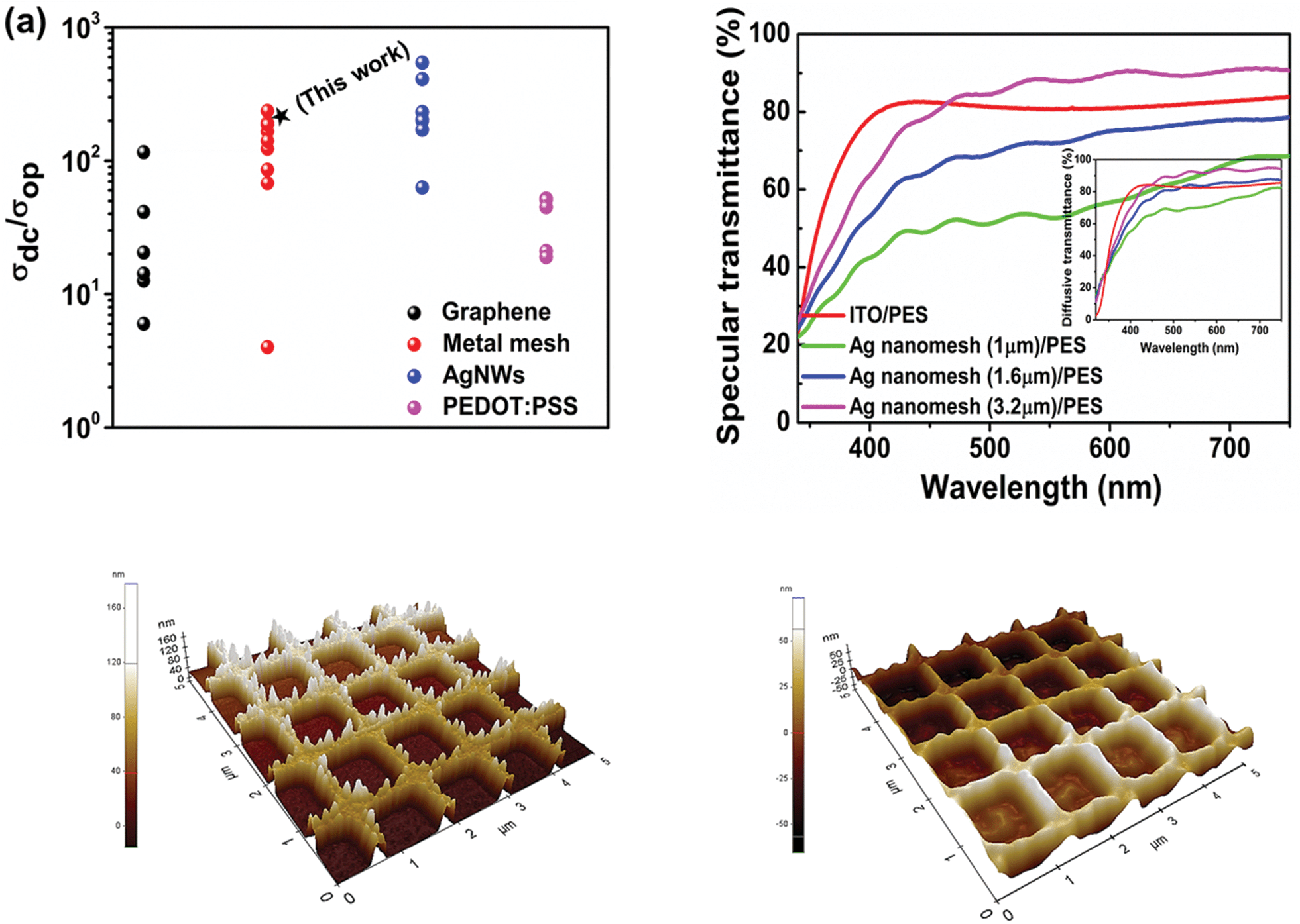 | ||
| Fig. 2 (a) DC-to-optical conductivity ratios (σDC/σOp) for emerging transparent conducting electrodes (TCEs). Data points are references respectively for graphene,12–17 PEDOT:PSS,18–22 Ag NWs,23–28 and metal mesh29–37 from the lowest to the highest. (b) Specular transmittance spectra for ITO/PES, and different line spacings of Ag nanomesh electrodes. AFM images (5 μm × 5 μm) of the Ag nanomesh electrode before (c) and after ZnO coating (d). | ||
We would like to point out that these values, as shown in Fig. 2(a), are much higher than those recently reported for graphene,12–17 conducting PEDOT:PSS,18–22 and Ag mesh29–36 TCEs. The specular transmittance (Tspec) and diffusive transmittance (Tdiff) of Ag nanomesh electrodes were compared with those of the sputtered ITO on PES, as shown in Fig. 2(b) and its inset. The transmittance measurement included the substrates. The optical and electrical properties of the various Ag nanomesh electrodes are summarized in Table 1. The sputtered ITO films had a Tspec of 81% at 550 nm and an average Tspec of 80% at wavelengths above the visible range. The average Tspec values of Ag nanomesh electrodes with 1.0, 1.6, and 3.2 μm line spacing at 550 nm were 56, 70, and 82%, respectively. In addition, the sheet resistance values (Rsh) of the Ag nanomesh on the PES substrate with 1.0, 1.6, and 3.2 μm line spacing were 4.1 ± 1.7, 7.5 ± 2.4, and 15.2 ± 2.8 Ω sq−1, respectively. From this result, the Tspec and Rsh appear to depend on the line spacing of the nanomesh pattern. When evaluating TCEs for solar cell applications, the diffusive transmittance, Tdiff, is a more important parameter than the specular transmittance, Tspec.
| Substrate | Sheet resistance (Ω sq−1) | Specular transmittance (%, @550 nm) | Diffusive transmittance (%, @550 nm) | FoM |
|---|---|---|---|---|
| Ag nanomesh (1 μm)/PES | 4.1 ± 1.7 | 52.7 | 69.9 | 123 |
| Ag nanomesh (1.6 μm)/PES | 7.5 ± 2.4 | 71.9 | 83.8 | 141 |
| Ag nanomesh (3.2 μm)/PES | 15.2 ± 2.8 | 88.1 | 92.4 | 187 |
For all the electrodes measured, Tdiff was higher than Tspec; this result corresponded with those found in previous studies.27,28,42 For instance, an Ag nanomesh electrode with a line spacing of 1.6 μm (Tdiff,550nm ≈ 83.85% at Rsheet ≈ 7.5 ± 2.4 Ω sq−1) exhibited a higher transparency than a 100 nm thick ITO film on a PES substrate (Tdiff,550nm ≈ 82.34% at Rsheet ≈ 35 ± 1.1 Ω sq−1). Fig. 2(c) and (d) show atomic force microscopy (AFM) images of the Ag nanomesh electrode on a PES substrate and that of a ZnO-coated Ag nanomesh electrode, respectively. The root-mean-square (RMS) of surface roughness was 31 nm for the Ag nanomesh electrode, resulting in the presence of a protruding Ag nanomesh, which produces localized height elevations that in turn create a high probability of electrical short circuiting. However, with a subsequent deposition of a ZnO buffer layer, the RMS surface roughness of the Ag nanomesh electrodes decreased to 12 nm, since the ZnO buffer layer partially filled the empty space in the nanomesh. Therefore, the reduced surface roughness of Ag nanomesh electrodes decreases the possibility of device short failure.
To evaluate the potential use of the prepared Ag nanomesh electrodes as TCEs in IOSCs, we fabricated IOSCs with the following configuration: (PES or glass)/ZnO/photoactive layer/PEDOT:PSS/Ag. The photoactive layer is a bulk heterojunction blend consisting of PTB7 as electron donors, and PC71BM as electron acceptors. A cross-section SEM image of an Ag nanomesh electrode, with a line spacing of 1.6 μm, fabricated on the PES substrate, and where uniform distribution of the component elements can clearly be observed, is shown in Fig. 3(a). Fig. 3(b) and (c) show a comparison of the current density versus voltage (J–V) characteristics and incident photon-to-current conversion efficiency (IPCE) spectra for both the flexible IOSCs with Ag nanomesh electrodes and ITO electrodes under AM 1.5G illumination conditions (see also Fig. S2†).
 | ||
| Fig. 3 (a) SEM image of the cross-section of a fabricated IOSC having the following structure: PES/Ag nanomesh/ZnO/PTB7:PC71BM/PEDOT:PSS/Ag and a 3D rendering of the device architecture. (b) Characteristic J–V curves of IOSCs fabricated on Ag nanomesh electrodes with PTB7:PC71BM photoactive layers under AM 1.5G illumination (100 mW cm−2). (c) IPCE spectra of the IOSCs with PTB7: PC71BM layers. (d) Stability comparison between the flexible IOSC-based ITO electrode and the Ag nanomesh electrode stored in air under ambient conditions. | ||
The key photovoltaic parameters such as short-circuit current density (Jsc), open-circuit voltage (Voc), fill factor (FF), and power and power conversion efficiency (PCE) are deduced from J–V characteristics and summarized in Table 2 (see also Fig. S3 and Table S1†). For instance, as shown in Fig. S3,† it is worth nothing that the IOSCs with Ag nanomesh electrodes (PES and glass) exhibited a PCE of ∼1.21% (Jsc ≈ 10.72 mA cm−2; Voc ≈ 0.40 V; FF ≈ 27.65%) and ∼1.69% (Jsc ≈ 12.45 mA cm−2; Voc ≈ 0.43 V; FF ≈ 31.99%), respectively.
| Device | J sc (mA cm−2) | V oc (V) | FF (%) | PCE (%) | R s (Ω cm2) | R sh (Ω cm2) | Integrated Jsc (mA cm−2) |
|---|---|---|---|---|---|---|---|
| ITO/PES | 16.05 ± 0.01 | 0.74 ± 0.03 | 61.81 ± 0.03 | 7.35 ± 0.08 | 4.37 ± 1.14 | 1.1 ± 1.2 × 10⁵ | 15.77 ± 0.31 |
| Ag nanomesh (1 μm)/PES | 14.66 ± 0.04 | 0.74 ± 0.01 | 61.52 ± 0.29 | 6.71 ± 0.10 | 5.36 ± 0.69 | 6.8 ± 1.1 × 10⁴ | 14.10 ± 0.23 |
| Ag nanomesh (1.6 μm)/PES | 16.03 ± 0.03 | 0.73 ± 0.01 | 60.89 ± 0.68 | 7.15 ± 0.08 | 5.67 ± 1.35 | 6.5 ± 0.7 × 10⁴ | 15.55 ± 0.18 |
| Ag nanomesh (3.2 μm)/PES | 16.52 ± 0.01 | 0.73 ± 0.01 | 58.16 ± 0.02 | 6.98 ± 0.02 | 5.94 ± 2.10 | 4.0 ± 1.0 × 10⁴ | 16.20 ± 0.21 |
| ITO/glass | 16.13 ± 0.03 | 0.75 ± 0.01 | 63.89 ± 0.89 | 7.69 ± 0.13 | 3.15 ± 0.97 | 2.3 ± 0.8 × 10⁵ | 15.80 ± 0.20 |
| Ag nanomesh (1 μm)/glass | 15.15 ± 0.03 | 0.74 ± 0.03 | 62.68 ± 0.10 | 7.05 ± 0.01 | 3.91 ± 1.05 | 6.1 ± 1.1 × 10⁴ | 14.89 ± 0.13 |
| Ag nanomesh (1.6 μm)/glass | 15.97 ± 0.09 | 0.74 ± 0.01 | 61.37 ± 0.42 | 7.25 ± 0.14 | 4.24 ± 1.38 | 5.9 ± 0.3 × 10⁴ | 15.52 ± 0.22 |
| Ag nanomesh (3.2 μm)/glass | 16.06 ± 0.18 | 0.73 ± 0.01 | 59.14 ± 1.34 | 6.97 ± 0.17 | 4.64 ± 1.50 | 3.5 ± 1.4 × 10⁴ | 15.41 ± 0.31 |
As expected, IOSCs without a ZnO layer show the formation of an S-shaped J–V curve, and low FF and Voc due to the occurrence of rectifying donor/acceptor (D/A) junctions between the photoactive layer and the Ag nanomesh electrode.27,43 For comparison, as can be seen in Fig. 3(b), we have fabricated IOSCs using a ZnO interlayer under the same conditions. The IOSCs with an Ag nanomesh electrode and a line spacing of 1.6 μm using a PTB7:PC71BM photoactive layer showed a PCE of ∼7.15% (Jsc ≈ 16.03 mA cm−2; Voc ≈ 0.73 V; FF ≈ 60.89%). The dramatic improvements in the performance of IOSCs with a ZnO interlayer can be attributed to the ohmic contact between the photoactive layer and the Ag nanomesh electrode and the facilitation of charge collection by the Ag nanomesh electrodes, and the reduced surface roughness of Ag nanomesh electrodes. All of the IOSCs with Ag nanomesh electrodes performed similarly to those using ITO films.
For example, the IOSCs with the ITO film and the Ag nanomesh electrode exhibited a PCE of ∼7.35% (Jsc ≈ 16.05 mA cm−2; Voc ≈ 0.74 V; FF ≈ 61.81%) and ∼7.15% (Jsc ≈ 16.03 mA cm−2; Voc ≈ 0.73 V; FF ≈ 60.89%), respectively. To the best of our knowledge, this result is the highest value reported to date for flexible OSCs based on metal mesh electrodes (Table S2†).
The reason for the slightly reduced PCE values for all the IOSCs with Ag nanomesh electrodes was the small decrease in their FF values. On the other hand, as the line spacing of the Ag nanomesh increased, the values of Jsc increased slightly; this is in accordance with well-established optical transmittance trends. We ascribe the reduced FF to the decreased Rsh and increased Rs in Ag nanomesh electrode-based IOSCs. To further investigate the hysteresis of IOSCs, the J–V characteristics of the IOSCs were measured in the dark under ambient conditions (Fig. S2(c) and (d)†). From this point of view, the rectification ratio of the IOSCs was calculated based on the J–V curves at ± 2.0 V. IOSCs based on Ag nanomesh electrodes with a line spacing of 1 μm, 1.6 μm, and 3.2 μm had rectification ratios of 2.7 × 10⁴, 1.9 × 10⁴, and 8.5 × 10³, respectively. Even though the high conductivity of Ag nanomesh electrodes is comparable with that of ITO/PES electrodes, these Ag nanomesh electrodes are not as continuous and smooth in terms of RMS roughness as the sputtered ITO films. The smaller line spacing of the Ag nanomesh electrode can lead to an efficient increase in the Rsh value and high rectification ratio, indicating a reduction in the leakage current and better charge collection efficiency.32,41,44
As shown in Fig. 3(c), the IPCE spectra of the IOSCs with Ag nanomesh electrodes in the range of 300–800 nm where the active layer mostly absorbs were very similar to those using the ITO/PES electrodes, indicating comparable device performance. For example, the Ag nanomesh electrode-based IOSCs with a line spacing of 1.6 μm were found to have an IPCE maximum of 71.42% at 540 nm and IOSCs with ITO/PES were found to have an IPCE maximum of 70.86% at the same wavelength.
Fig. 3(d) shows non-encapsulated IOSCs, with a structure of Ag nanomesh electrode/ZnO/PTB7:PC71BM/PEODT:PSS/Ag. These were stored in air under ambient conditions and their efficiency was measured periodically to check their long-term stability. The flexible IOSCs with the Ag nanomesh and ITO electrodes retained over ∼80% of the original efficiency after 30 days.
Fig. 4(a) shows a comparison of the changes in the Rsheet of electrodes using the Ag nanomesh/PES (Rsheet ≈ 7.5 Ω sq−1) with ITO/PES (Rsheet ≈ 35 Ω sq−1) films as a function of bending radius. The bending induced compressive stress in the electrodes, and each value shown is the average of five samples. The percent change in the resistance of electrodes is expressed as ΔΩ Ω0−1, where ΔΩ is the actual change in the resistance after bending and Ω0 is the initial resistance. The Ag nanomesh electrodes showed small ΔΩ Ω0−1 values (∼6.04 ± 2.29%), even after being bent with a radius of 1.49 mm, which corresponds to a bending strain (ε) of ∼6.7%, with ε = hs/(2R), where hs is the substrate thickness.45 On the other hand, ITO/PES electrodes exhibited a dramatic increase in ΔΩ Ω0−1 values (∼77.5 ± 2.87%).
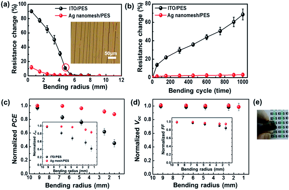 | ||
| Fig. 4 (a) Measured changes in the resistance of the electrodes based on flexible Ag nanomesh/PES and ITO/PES films as a function of the bending radius. Inset figure: optical image of the ITO/PES-film electrode after being bent with a radius of ∼4.8 mm. (b) Change in the resistance as a function of the number of bending cycles with bending radius (R) ≈ 5.5 mm. (c) The measured PCE, Jsc (inset). (d) Voc and FF (inset) values of the flexible Ag nanomesh/PES electrode-based IOSCs as a function of the bending radius during compressive bending, normalized to the initial value. (e) Photograph of an Ag nanomesh electrode-based IOSC. | ||
Furthermore, the Ag nanomesh electrode exhibited superior bending fatigue strength, as shown Fig. 4(b), where the bending radius was fixed at R ≈ 5.4 mm, which corresponded to ε ≈ 1.7%. Even after being bent 1000 times, the Ag nanomesh electrodes showed only a slight increase in ΔΩ Ω0−1 values (∼3.1 ± 0.8%), whereas those of the ITO/PES electrodes dramatically increased (∼68.5 ± 5.9%). Furthermore, we also performed oxidation-resistance and adhesion tests on the Ag nanomesh electrodes (Fig. S4†).
Fig. 4(c) and (d) show a comparison of the changes in the key factors for IOSCs based on Ag nanomesh electrodes and ITO/PES electrodes as a function of bending radius. The Ag nanomesh electrode-based IOSCs showed a small reduction of PCE after being bent significantly (R ≈ 1.49 mm). In contrast, the PCEs of the ITO/PES devices fell to below half of their initial values.
In conclusion, we developed a facile approach to successfully demonstrate highly transparent and flexible Ag nanomesh electrodes by combining nanoimprint lithography (NIL) and transfer printing without the use of a conducting polymer. The Ag nanomesh electrodes exhibited superior optical and electrical properties as well as mechanical flexibility. Furthermore, the flexible IOSCs fabricated with Ag nanomesh electrodes exhibited excellent photovoltaic performance as well as superior long-term stability under ambient conditions. If the new method for uniform Ag nanomesh electrodes is developed with a short manufacturing time, we believe that Ag nanomesh electrodes can be used as an alternative to ITO for emerging optoelectronic devices such as flexible solar cells and displays in the near future.39,40
Acknowledgements
This work was supported by the collaboration funds from KIMS (PKC1540) and KIMM (KM3460). This study was also supported by the Pioneer Research Center Program through the National Research Foundation of Korea funded by the Ministry of Science, ICT & Future Planning (NRF-2013M3C1A3065528).Notes and references
- F. C. Krebs, T. Tromholt and M. Jørgensen, Nanoscale, 2010, 2, 873–886 RSC.
- F. C. Krebs, J. Fyenbo and M. Jørgensen, J. Mater. Chem., 2010, 20, 8994–9001 RSC.
- F. C. Krebs, T. D. Nielsen, J. fyenbo, M. Wadstrøm and M. S. Pedersen, Energy Environ. Sci., 2010, 3, 512–525 CAS.
- M. Song, J. W. Kang, D. H. Kim, J. D. Kwon, S. G. Park, S. Nam, S. Jo, S. Y. Ryu and C. S. Kim, Appl. Phys. Lett., 2013, 102, 143303 CrossRef PubMed.
- Z. C. He, C. M. Zhong, S. J. Su, M. Xu, G. B. Wu and Y. Cao, Nat. Photonics, 2012, 6, 591–595 Search PubMed.
- Z. Xu, L. M. Chen, G. Yang, C. H. Huang, J. Hou, Y. Wu, G. Li, C. S. Hus and Y. Yang, Adv. Funct. Mater., 2009, 19, 1227–1234 CrossRef CAS.
- H. L. yip and A. K. Y. Jen, Energy Environ. Sci., 2012, 5, 5994–6011 CAS.
- F. C. Krebs and K. Norman, Prog. Photovoltaics, 2007, 15, 697–712 CAS.
- J. H. Huang, J. H. Fang, C. C. Liu and C. W. Chu, ACS Nano, 2011, 5, 6262–6271 CrossRef CAS PubMed.
- T. Chen, S. Wang, Z. Yang, Q. Feng, X. Sun, L. Li, Z. S. Wang and H. Peng, Angew. Chem., Int. Ed., 2011, 50, 1815–1819 CrossRef CAS PubMed.
- J. M. Lee, J. S. Park, S. H. Lee, H. Kim, S. Yoo and S. O. Kim, Adv. Mater., 2011, 23, 629–633 CrossRef CAS PubMed.
- U. Khan, A. O'Neill, M. Lotya, S. De and J. N. Coleman, Small, 2010, 6, 864–871 CrossRef CAS PubMed.
- K. S. Kim, Y. Zhao, H. Jang, S. Y. Lee, J. M. Kim, K. S. Kim, J. H. Ahn, P. Kim, J. Y. Choi and B. H. Hong, Nature, 2009, 457, 706–710 CrossRef CAS PubMed.
- C. L. Hsu, C. T. Lin, J. H. Huang, C. W. Chu, K. H. Wei and L. J. Li, ACS Nano, 2012, 6, 5031–5039 CrossRef CAS PubMed.
- S. Bae, H. Kim, Y. Lee, X. Xu, J.-S. Park, Y. Zheng, J. Balakrishnan, T. Lei, H. R. Kim, Y. I. Song, Y. J. Kim, K. S. Kim, B. Ozyilmaz, J. H. Ahn, B. H. Hong and S. Iijima, Nat. Nanotechnol., 2010, 5, 574–578 CrossRef CAS PubMed.
- F. Günes, H. J. Shin, C. Biswas, G. H. Han, E. S. Kim, S. J. Chae, J. Y. Choi and Y. H. Lee, ACS Nano, 2010, 8, 4595–4600 CrossRef PubMed.
- Y. Lee, S. Bae, H. Jang, S. Jang, S. E. Zhu, S. H. Sim, Y. I. Song, B. H. Hong and J. H. Ahn, Nano Lett., 2010, 10, 490–493 CrossRef CAS PubMed.
- S. I. Na, G. Wang, S. S. Kim, T. W. Kim, S. H. Oh, B. K. Yu, T. Lee and D. Y. Kim, J. Mater. Chem., 2009, 19, 9045–9053 RSC.
- M. Vosgueritchian, D. J. Lipomi and Z. Bao, Adv. Funct. Mater., 2012, 22, 421–428 CrossRef CAS .9.
- Y. Xia, K. Sun and J. Ouyang, Energy Environ. Sci., 2012, 5, 5325–5332 CAS.
- W. Zhang, B. Zhao, Z. He, X. Zhao, H. Wang, S. Yang, H. Wu and Y. Cao, Energy Environ. Sci., 2013, 6, 1956 CAS.
- Y. H. Kim, J. Lee, S. Hofmann, M. C. Gather, L. M. Meskamp and K. Leo, Adv. Funct. Mater., 2013, 23, 3763–3769 CrossRef CAS.
- J. Y. Lee, S. T. Connor, Y. Cui and P. Peumans, Nano Lett., 2008, 8, 689–692 CrossRef CAS PubMed.
- S. De, T. M. Higgins, P. E. Lyons, E. M. Doherty, P. N. Nirmalraj, W. J. Blau, J. J. Boland and J. N. Coleman, ACS Nano, 2009, 3, 1767–1774 CrossRef CAS PubMed.
- W. Gaynor, G. F. Burkhard, M. D. McGehee and P. Peumans, Adv. Mater., 2011, 23, 2905–2910 CrossRef CAS PubMed.
- D. S. Leem, A. Edwards, M. Faist, J. Nelson, D. D. C. Bradley and J. C. de Mello, Adv. Mater., 2011, 23, 4371–4375 CrossRef CAS PubMed.
- M. Song, J. H. Park, C. S. Kim, D. H. Kim, Y. C. Kang, S. H. Jin, W. Y. Jin and J. W. Kang, Nano Res., 2014, 7, 1370–1379 CrossRef CAS PubMed.
- M. Song, D. S. You, K. Lim, S. Park, S. Jung, C. S. Kim, D. H. Kim, D. G. Kim, J. K. Kim, J. Park, Y. C. Kang, J. Heo, S. H. Jin, J. H. Park and J. W. Kang, Adv. Funct. Mater., 2013, 23, 4177–4184 CrossRef CAS.
- S. Hong, J. Yeo, G. Kim, D. Kim, H. Lee, J. Kwon, H. Lee, P. Lee and S. H. Ko, ACS Nano, 2013, 6, 5024–5031 CrossRef PubMed.
- M. G. Kang and L. J. Guo, Adv. Mater., 2007, 19, 1391–1396 CrossRef CAS.
- M. G. Kang, M. S. Kim, J. Kim and L. J. Guo, Adv. Mater., 2008, 20, 4408–4413 CrossRef CAS.
- J. Zou, H. L. Yip, S. K. Hau and A. K. Y. Jen, Appl. Phys. Lett., 2010, 96, 203301–203303 CrossRef PubMed.
- N. Kwon, K. Kim, S. Sung, I. Yi and I. Chung, Nanotechnology, 2013, 24, 235205–235212 CrossRef CAS PubMed.
- J. Woerle and H. Rost, MRS Bull., 2011, 36, 789–793 CrossRef CAS.
- J. G. Ok, M. K. Kwak, C. M. Huard, H. S. Youn and L. J. Guo, Adv. Mater., 2013, 25, 6554–6561 CrossRef CAS PubMed.
- P. Kuang, J. M. Park, W. Leung, R. C. Mahadevapuram, K. S. Nalwa, T. G. Kim, S. Chaudhary, K. M. Ho and K. Constant, Adv. Mater., 2011, 23, 2469–2473 CrossRef CAS PubMed.
- J. S. Yu, G. H. Jung, J. Jo, J. S. Kim, J. W. Kim, S. W. Kwak, J. L. Lee, I. Kim and D. Kim, Sol. Energy Mater. Sol. Cells, 2013, 109, 142–147 CrossRef CAS PubMed.
- J. S. Yu, I. Kim, J. S. Kim, J. Jo, T. T. Larsen-Olsen, R. R. Søndergaard, M. Hösel, D. Angmo, M. Jørgensen and F. C. Krebs, Nanoscale, 2012, 4, 6032–6040 RSC.
- M. Hösel, R. R. Søndergaard, M. Jørgensen and F. C. Krebs, Energy Technol., 2013, 1, 102–107 CrossRef.
- F. C. Krebs, N. Espinosa, M. Hösel, R. R. Søndergaard and M. Jørgensen, Adv. Mater., 2014, 26, 29–39 CrossRef CAS.
- M. Dressel and G. Grüner, Electrodynamics of Solids, Cambridge University Press, Cambridge, 2002 Search PubMed.
- H. Wu, L. Hu, M. W. Rowell, D. Kong, J. J. Cha, J. R. McDonough, J. Zhu, Y. Yang, M. D. McGehee and Y. Cui, Nano Lett., 2010, 10, 4242–4248 CrossRef CAS PubMed.
- O. J. Sandberg, M. Nyman and R. Österbacka, Phys. Rev. A: At., Mol., Opt. Phys., 2014, 1, 024003 Search PubMed.
- N. Li, B. E. Lassiter, R. R. Lunt, G. D. Wei and S. R. Forrest, Appl. Phys. Lett., 2009, 94, 023307 CrossRef PubMed.
- S. I. Park, J. H. Ahn, X. Feng, S. Wang, Y. Huang and J. A. Rogers, Adv. Funct. Mater., 2008, 18, 2673–2684 CrossRef CAS.
Footnotes |
| † Electronic supplementary information (ESI) available: A description of the detailed experimental process, SEM images of the Ag nanomesh, Characteristic J–V curves, dark J–V curves, and IPCE spectra, SEM images of the Ag nanomesh during the oxidation test, and optical simulation of devices. See DOI: 10.1039/c4ta05294c |
| ‡ These authors contributed equally to this paper. |
| This journal is © The Royal Society of Chemistry 2015 |