Competition between electron doping and short-range scattering in hydrogenated bilayer graphene on hexagonal boron nitride

S. J. Honga, H. Kanga, M. Parkb, M. Leec, D. Soler-Delgadoa, D. H. Jeongc, Y. W. Park*a and B. H. Kim*d
aDepartment of Physics and Astronomy, Seoul National University, Seoul 151-747, Republic of Korea. E-mail: ywpark@phya.snu.ac.kr
bDepartment of Nano Science and Technology, Seoul National University, Seoul 151-747, Republic of Korea
cDepartment of Chemistry Education, Seoul National University, Seoul 151-742, Republic of Korea
dDepartment of Physics, Incheon National University, Incheon 406-772, Republic of Korea. E-mail: kbh37@inu.ac.kr

Received 15th September 2015 , Accepted 23rd November 2015

First published on 24th November 2015


Abstract

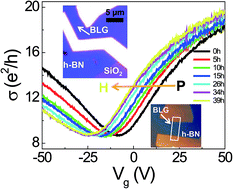
We studied the electron doping of bilayer graphene (BLG) on hexagonal boron nitride (h-BN) by dissociative H2 adsorption. Charge transfer phenomena were investigated by the gate voltage (Vg)-dependent electrical conductivity σ(Vg) and Raman spectroscopy with respect to the H2 exposure. The shift of the charge neutrality point toward the negative Vg region was observed and the charge scattering mechanism was found with the variation of σ(Vg). The charge transfer at the interface as well as the lattice distortion of BLG due to hydrogenation were verified by Raman spectroscopy. From these results, we concluded that the electron doping and short-range scattering in the BLG exposed to high H2 pressure (11 bar) are intrinsic features, which were achieved using a van der Waals interface consisting of BLG and h-BN.


1. Introduction

In contrast to the linear dispersion of single-layer graphene (SLG), bilayer graphene (BLG), which consists of two graphene sheets with Bernal stacking, has a parabolic electronic band structure.1,2 Given that the electronic band gap of BLG can be opened by applying a perpendicular electric field which breaks the inversion symmetry, extensive research has been carried out via dual-gated configurations3,4 and asymmetric chemical doping.5–8 With band gap engineering, the realization of n-type BLG transistors is essential for graphene-based electronics such as complementary logic devices.6 Various methods have been applied to achieve n-type graphene.6–9 Hydrogenation is one of the approaches which can be used to functionalize graphene10–15 and reportedly provides an n-type dopant in graphene layers.12–14 Using the electron doping properties due to dissociative H2 adsorption,14 a p–n junction has also been realized in SLG devices.16 In contrast, few investigations of hydrogenated BLG have been done in spite of its considerable applicability.

It is known that adsorption on a graphene-based system can be related in an extrinsic environment and through intrinsic chemical interaction. Thus, as adsorption with I2 (ref. 17 and 18) and O2 (ref. 19 and 20) is carried out, the interface between graphene and the underlying SiO2 is a crucial for the variation of the electrical properties. Chu et al. noted that intercalated halogen molecules screen charge impurities which are embedded in SiO2.18 Silvestre et al. also reported that interfacial O2 decreases the scattering due to defects and corrugations in the substrate and increases the average distance between charge carriers and substrate impurities.20 Meanwhile, hexagonal boron nitride (h-BN) has attracted attention as a building block for two-dimensional devices because h-BN substrates play an important role in eliminating the substrate effect, thus enabling intrinsic electronic properties.21–29 Furthermore, the interface between graphene and h-BN, i.e., the van der Waals interface, is tight enough to provide a seal against adsorbate intercalation.29,30 Therefore, the BLG/h-BN device structure has become a platform on which to access intrinsic chemical-reacted phenomena.

Here, we report dissociative H2 adsorption on BLG supported by an h-BN substrate. As with SLG, electron doping was observed in BLG/h-BN, which was probed by the gate voltage-dependent electrical conductivity σ(Vg) and Raman spectroscopy. The variation of the mobility (μ) and the minimum conductivity (σmin) upon H2 exposure provide information about the scattering mechanism. The Raman spectroscopy results show that the compressive lattice strain and the charge transfer both contribute significantly to the electronic transport properties of hydrogen adsorbed BLG. We expect that the hydrogenation of BLG is a key step in the realization of n-type transistors for graphene-based electronics.

2. Experimental

The BLG/h-BN device was fabricated by a conventional exfoliation and transfer process.21 High-quality h-BN (HQ-graphene) was exfoliated on a SiO2 (285 nm)/Si substrate. A thickness of 10 nm was measured by an atomic force microscope (AFM). The BLG was exfoliated from HOPG (SPI supplies) and transferred by means of micro-alignment. The BLG was then identified by Raman spectroscopy with a 532 nm laser (LabRam 300, JY-Horiba). A standard electron beam lithography process and metal evaporation (Cr/Au = 5/50 nm) were also used. A pristine device was obtained by annealing at 380 K under a high vacuum (∼5 × 10⁻⁶ Torr) for 10 hours using home-made high temperature and high pressure chamber. The σ(Vg) with a three-terminal configuration was measured using 4200-SCS Keithley semiconductor analyzer under H2 exposure at a pressure of 11 bar (99.9999%) at 350 K. The DC bias voltage (Vds) was fixed to 1 mV and the electrical current (Ids) was measured as a function of back gate voltage (Vg). With fixed H2 pressure and temperature, the σ(Vg) measurements were performed as exposed time.

3. Results and discussion

Fig. 1 shows σ(Vg) of BLG/h-BN as a function of the H2 exposure time. The black curve corresponding to σ(Vg) of the pristine BLG/h-BN shifted to the negative Vg region and was finally saturated to the yellow curve in the Fig. 1. The electron doping due to H2 adsorption was consistent with a previous experiment on BLG on SiO2 substrates.14 The inset indicates optical (top) and AFM (bottom) images of the BLG/h-BN device, respectively.
image file: c5ra18945d-f1.tif
Fig. 1 The conductivity (σ) versus gate voltage (Vg) curves of BLG/h-BN as H2 exposure time. Insets show optical (top) and AFM (bottom) image of BLG/h-BN device. P and H denote pristine and H2 treated case, respectively.

The electronic transport properties were investigated by the temporal evolution of the charge neutrality point (VCNP) and the electron/hole mobility (μe and μh, respectively) (Fig. 2). Fig. 2a shows the variation of VCNP (black squares) due to H2 exposure and the fitting curve (red line). The negative shift of VCNP is direct evidence of electron doping in BLG/h-BN, which can be understood as a charge transfer due to dissociative H2 adsorption.14 The adsorption is saturated to a certain degree because the number of pre-existing interaction sites determines the saturation coverage.12 The temporal dependence of VCNP can be described by a first-order Langmuir-type adsorption model, −ΔVCNP = −ΔVSatCNP(1 − ekt), where −ΔVSatCNP and k are the magnitude of the saturated VCNP and the kinetic coefficient, respectively. This type of first-order adsorption has been widely observed in SLG and BLG regardless of the adsorbate type used, such as H2, O2, or NH3.12,20,31 We obtained values of 18 V and 0.05 h−1 for each fitting parameter and a value of 0.994 for the adj. R2.


image file: c5ra18945d-f2.tif
Fig. 2 Temporal evolution of (a) the charge neutrality point, VCNP, (b) electron/hole mobility, μe and μh, and (c) −ΔVCNP versus 1/μ. The black and red lines are guide for eye. (d) The minimum conductivity, σmin versus −ΔVCNP.

We observed reductions of μe and μh, of which the carrier densities correspond to VCNP ±10 V, respectively with H2 adsorption as shown in Fig. 2b. The field effect mobility was determined via image file: c5ra18945d-t1.tif, where cg is the back gate capacitance per unit area. It was found that O2 adsorption on BLG/SiO2 enhances the mobility asymmetry between μe and μh. Silvestre et al.20 reported that interfacial O2 between BLG and SiO2 contributes to an increase of μe and μh due to the screening of embedded impurities in the substrate, while the μe decreases due to short-range scattering, as anticipated by the resonant states above CNP through density functional theory calculations.20 Likewise, we reported mobility asymmetry (increased μe and decreased μh) in SLG and BLG on SiO2 substrates during H2 adsorption.14 Considering that the BLG device in this study was fabricated on a h-BN substrate, which is known to mitigate the effects of embedded impurities in SiO2 substrate, the extrinsic factor for increasing mobility can be excluded. Therefore, the mobility reduction is in good agreement with earlier research on hydrogenated single-layer graphene (SLG).12

The impurity density, nimp is proportional to −ΔVCNP, image file: c5ra18945d-t2.tif, where e is the charge element.20 It has been theoretically reported that the short-range scattering in BLG yields mobility which is inversely proportional to nimp.32 In Fig. 2c, image file: c5ra18945d-t3.tif for electron and hole corresponding to VCNP ±10 V, has a linear relationship with −ΔVCNP, that is image file: c5ra18945d-t4.tif. It should be noted that the image file: c5ra18945d-t5.tif behavior in BLG is not a sufficient but a necessary condition to confirm short-range scattering, as the same behavior is expected during long-range scattering.9 However, chemisorbed H atoms on graphene are generally known to be short-range scatterers.12,31,32 Furthermore, the results of a Raman study, which will be discussed below, show definite C–H bonding which promotes short-range scattering.32 Therefore, the condition of image file: c5ra18945d-t6.tif in BLG due to H2 dissociative adsorption reveals that the hydrogenation results in the short-range scattering in BLG as well as SLG.12,33

The minimum conductivity in SLG, σmin depending on nimp, shows various behaviors depending on the type of adsorbate. K, Ti, and Pt doping induce a reduced σmin, while σmin remains constant after Au and Fe doping.34–36 Chu et al. noted that various σmin behaviors can be explained by the competition between the mobility and induced carrier density, n0 (i.e., σminμn0).18 This type of competitive behavior was also observed during H2 adsorption, during which σmin decreases12 or increases.37 Fig. 2d shows a nearly constant σmin with H2 adsorption, which can be understood by balancing μ and n0.

Fig. 3a shows the Raman spectra acquired before (black) and after (red) H2 exposure, showing typical G and 2D peaks for BLG as well as h-BN (1366 cm−1) peak. After H2 exposure, the D + G mode (2935 cm−1) in Fig. 3a, the D (1350 cm−1) and D′ (1620 cm−1) peaks in Fig. 3b were developed. These D and D′ peaks indicate successful hydrogenation on BLG/h-BN.10–15,33 The D + G mode is also evidence of hydrogenation, which results in C–H bonds.11,14,15 The typical Raman spectra in BLG also provide significant information related to the atomic structure and charge transfer properties. Similar to SLG, the peak position and full width half maximum (FWHM) of the Raman spectra in BLG are sensitive to the charge carrier density38 and the lattice strain.39,40 The G peak position (ωG) and the FWHM (ΓG), for pristine BLG/h-BN are 1582.7 cm−1 and 13.8 cm−1, respectively, as shown by the black curve in Fig. 3c. The values of ωG and ΓG indicate that the Fermi energy of BLG/h-BN is initially close to the CNP.38 The Raman G peak results are in good agreement with σ(Vg), as shown in Fig. 1, where VCNP is close to zero for the pristine case. The G peak after the H2 treatment was blue-shifted and broadened; that is, ωG and ΓG are 1584.2 cm−1 and 21.1 cm−1, respectively, as denoted by the blue curves in Fig. 3c. In contrast, the 2D peak position (ω2D) is red-shifted, as shown in Fig. 3d. The upper plot in Fig. 3d shows the 2D peak of pristine BLG, which consists of multi-components, 2D1A, 2D1B, 2D2A and 2D2B. We observed that all components became red-shifted after H2 adsorption, as shown in the lower plot of Fig. 3d. Specifically, the 2D1A and 2D2A peak positions changed from 2689 cm−1 and 2708 cm−1 to 2679 cm−1 and 2698 cm−1, respectively. In a previous study, these two components were at 2690 cm−1 and 2710 cm−1 at the CNP.38 Upon electron doping, these positions are both monotonically red-shifted. These G and 2D peak shifts collectively indicate electron doping, consistent with the results of σ(Vg). On the one hand, the FWHM of the G peak increased from 13.8 cm−1 to 21.1 cm−1 after H2 exposure. In the unstrained case, the FWHM of BLG is limited below ∼14 cm−1 at a wide charge carrier density range, |EF| < 0.2 eV.38 On the other hand, the G peak broadens and is finally separated by the G+ and G modes under tensile or compressive strain.40 Furthermore, we observed that dissociative H2 adsorption results in compressive strain in SLG.14 Thus, the increase in the FWHM can be explained by the introduction of compressive lattice strain. Finally, we note that the Raman 2D peak maintained a multi-component structure after the H2 treatment, which means that decoupling due to intercalation between the graphene layers was not detected during H2 adsorption on BLG.


image file: c5ra18945d-f3.tif
Fig. 3 (a–d) The black/red curves correspond to the Raman spectra acquired before/after H2 exposure, respectively. (a) Full spectra, enlarged regions of (b) h-BN, D and D′ peaks, (c) G peak, and (d) 2D peak. All blue curves in (c and d) are single Lorentzians formulated to fit a multi-component spectrum.

4. Conclusions

In summary, we investigated the intrinsic electron doping and short-range scattering phenomena in BLG upon dissociative H2 adsorption. The results were achieved using the van der Waals interface with the BLG/h-BN structure. We observed (i) a negative shift of VCNP, (ii) saturating behavior of electron doping, (iii) inverse nimp-dependent mobility, and (iv) σmin with competition between the mobility and the induced carrier density. The results are consistent with the Raman spectra which show hydrogenation of the carbon structure. These fundamental studies are expected to contribute to carbon electronics.

Acknowledgements

This work was supported by the Swedish-Korean Basic Research Cooperative Program (No. 2014R1A2A1A12067266) of the NRF, Korea. M.L. and D.H.J. acknowledge the support of the Pioneer Research Center Program through the NRF of Korea, funded by the Ministry of Science, ICT & Future Planning (No. NRF-2011-0027888). B.H.K. acknowledges the support from the National Research Foundation of Korea (No. NRF-2014R1A1A1002467).

Notes and references

  1. E. McCann and V. I. Fal'ko, Phys. Rev. Lett., 2006, 96, 086805 CrossRef PubMed.
  2. K. S. Novoselov, E. McCann, S. V. Morozov, V. I. Fal'ko, M. I. Katsnelson, U. Zeitler, D. Jiang, F. Schedin and A. K. Geim, Nat. Phys., 2006, 2, 177 CrossRef.
  3. J. B. Oostinga, H. B. Heersche, X. Liu, A. F. Morpurgo and L. M. K. Vandersypen, Nat. Mater., 2008, 7, 151 CrossRef CAS PubMed.
  4. Y. Zhang, T. T. Tang, C. Girit, Z. Hao, M. C. Martin, A. Zettl, M. F. Crommie, Y. R. Shen and F. Wang, Nature, 2009, 459, 820 CrossRef CAS PubMed.
  5. W. Zhang, C. T. Lin, K. K. Liu, T. Tite, C. Y. Su, C. H. Chang, Y. H. Lee, C. W. Chu, K. H. Wei, J. L. Kuo and L. J. Li, ACS Nano, 2011, 5, 7517 CrossRef CAS PubMed.
  6. W. J. Yu, S. H. Chae, Y. H. Lee and X. Duan, Nano Lett., 2011, 11, 4759 CrossRef CAS PubMed.
  7. J. Park, S. B. Jo, Y. J. Yu, Y. Kim, J. W. Yang, W. H. Lee, H. H. Kim, B. H. Hong, P. Kim, K. Cho and K. S. Kim, Adv. Mater., 2012, 24, 407 CrossRef CAS PubMed.
  8. A. J. Samuels and J. D. Carey, ACS Nano, 2013, 7, 2790 CrossRef CAS PubMed.
  9. S. Xiao, J. H. Chen, S. Adam, E. D. Williams and M. S. Fuhrer, Phys. Rev. B: Condens. Matter Mater. Phys., 2010, 82, 041406 CrossRef.
  10. S. Ryu, M. Y. Han, J. Maultzsch, T. F. Heinz, P. Kim, M. L. Steigerwald and L. E. Brus, Nano Lett., 2008, 8, 4597 CrossRef CAS PubMed.
  11. D. C. Elias, R. R. Nair, T. M. G. Mohiuddin, S. V. Morozov, P. Blake, M. P. Halsall, A. C. Ferrari, D. W. Boukhvalov, M. I. Katsnelson, A. K. Geim and K. S. Novoselov, Science, 2009, 323, 610 CrossRef CAS PubMed.
  12. J. Katoch, J. H. Chen, R. Tsuchikawa, C. W. Smith, E. R. Mucciolo and M. Ishigami, Phys. Rev. B: Condens. Matter Mater. Phys., 2010, 82, 081417 CrossRef.
  13. B. R. Matis, J. S. Burgess, F. A. Bulat, A. L. Friedman, B. H. Houston and J. W. Baldwin, ACS Nano, 2012, 6, 17 CrossRef CAS PubMed.
  14. B. H. Kim, S. J. Hong, S. J. Baek, H. Y. Jeong, N. Park, M. Lee, S. W. Lee, M. Park, S. W. Chu, H. S. Shin, J. Lim, J. C. Lee, Y. Jun and Y. W. Park, Sci. Rep., 2012, 2, 690 Search PubMed.
  15. R. Jayasingha, A. Sherehiy, S. Y. Wu and G. U. Sumanasekera, Nano Lett., 2013, 13, 5098 CrossRef CAS PubMed.
  16. M. Park, Y. J. Yun, M. Lee, D. H. Jeong, Y. Jun, Y. W. Park and B. H. Kim, AIP Adv., 2015, 5, 017120 CrossRef.
  17. N. Jung, A. C. Crowther, N. Kim, P. Kim and L. E. Brus, ACS Nano, 2010, 4, 7005 CrossRef CAS PubMed.
  18. S. W. Chu, S. J. Baek, D. C. Kim, S. Seo, J. S. Kim and Y. W. Park, Synth. Met., 2012, 162, 1689 CrossRef CAS.
  19. Y. Sato, K. Takai and T. Enoki, Nano Lett., 2011, 11, 3468 CrossRef CAS PubMed.
  20. I. Silvestre, E. A. de Morais, A. O. Melo, L. C. Campos, A.-M. B. Goncalves, A. R. Cadore, A. S. Ferlauto, H. Chacham, M. S. C. Mazzoni and R. G. Lacerda, ACS Nano, 2013, 7, 6597 CrossRef CAS PubMed.
  21. C. R. Dean, A. F. Young, I. Meric, C. Lee, L. Wang, S. Sorgenfrei, K. Watanabe, T. Taniguchi, P. Kim, K. L. Shepard and J. Hone, Nat. Nanotechnol., 2010, 5, 722 CrossRef CAS PubMed.
  22. J. Xue, J. Sanchez-Yamagishi, D. Bulmash, P. Jacquod, A. Deshpande, K. Watanabe, T. Taniguchi, P. Jarillo-Herrero and B. J. LeRoy, Nat. Mater., 2011, 10, 282 CrossRef CAS PubMed.
  23. L. H. Li, E. J. G. Santos, T. Xing, E. Cappelluti, R. Roldán, Y. Chen, K. Watanabe and T. Taniguchi, Nano Lett., 2015, 15, 218 CrossRef CAS PubMed.
  24. P. J. Zomer, M. H. D. Guimarães, N. Tombros and B. J. van Wees, Phys. Rev. B: Condens. Matter Mater. Phys., 2012, 86, 161416(R) CrossRef.
  25. M. H. D. Guimarães, P. J. Zomer, J. Ingla-Aynés, J. C. Brant, N. Tombros and B. J. van Wees, Phys. Rev. Lett., 2014, 113, 086602 CrossRef PubMed.
  26. M. V. Kamalakar, A. Dankert, J. Bergsten, T. Ive and S. P. Dash, Appl. Phys. Lett., 2014, 105, 212405 CrossRef.
  27. M. V. Kamalakar, A. Dankert, J. Bergsten, T. Ive and S. P. Dash, Sci. Rep., 2014, 4, 6146 CrossRef CAS PubMed.
  28. M. Drögeler, F. Volmer, M. Wolter, B. Terrés, K. Watanabe, T. Taniguchi, G. Güntherodt, C. Stampfer and B. Beschoten, Nano Lett., 2014, 14, 6050 CrossRef PubMed.
  29. L. Wang, Z. Chen, C. R. Dean, T. Taniguchi, K. Watanabe, L. E. Brus and J. Hone, ACS Nano, 2012, 6, 9314 CrossRef CAS PubMed.
  30. Z. Chen, P. Darancet, L. Wang, A. C. Crowther, Y. Gao, C. R. Dean, T. Taniguchi, K. Watanabe, J. Hone, C. A. Marianetti and L. E. Brus, ACS Nano, 2014, 8, 2943 CrossRef CAS PubMed.
  31. S. Chen, W. Cai, D. Chen, Y. Ren, X. Li, Y. Zhu, J. Kang and R. S. Ruoff, New J. Phys., 2010, 12, 125011 CrossRef.
  32. A. Ferreira, J. Viana-Gomes, J. Nilsson, E. R. Mucciolo, N. M. R. Peres and A. H. Castro Neto, Phys. Rev. B: Condens. Matter Mater. Phys., 2011, 83, 165402 CrossRef.
  33. J. Balakrishnan, G. K. W. Koon, M. Jaiswal, A. H. Castro Neto and B. Özyilmaz, Nat. Phys., 2013, 9, 284 CrossRef CAS.
  34. J.-H. Chen, C. Jang, S. Adam, M. S. Fuhrer, E. D. Williams and M. Ishigami, Nat. Phys., 2008, 4, 377 CrossRef CAS.
  35. K. Pi, K. M. McCreary, W. Bao, W. Han, Y. F. Chiang, Y. Li, S. W. Tsai, C. N. Lau and R. K. Kawakami, Phys. Rev. B: Condens. Matter Mater. Phys., 2009, 80, 075406 CrossRef.
  36. K. M. McCreary, K. Pi, A. G. Swartz, W. Han, W. Bao, C. N. Lau, F. Guinea, M. I. Katsnelson and R. K. Kawakami, Phys. Rev. B: Condens. Matter Mater. Phys., 2010, 81, 115453 CrossRef.
  37. S. J. Hong, M. Park, H. Kang, M. Lee, D. Soler-Delgado, D. S. Shin, K. H. Kim, S. Kubatkin, D. H. Jeong, Y. W. Park and B. H. Kim, Appl. Phys. Lett., 2015, 106, 142110 CrossRef.
  38. A. Das, B. Chakraborty, S. Piscanec, S. Pisana, A. K. Sood and A. C. Ferrari, Phys. Rev. B: Condens. Matter Mater. Phys., 2009, 79, 155417 CrossRef.
  39. Z. H. Ni, H. M. Wang, Y. Ma, J. Kasim, Y. H. Wu and Z. X. Shen, ACS Nano, 2008, 2, 1033 CrossRef CAS PubMed.
  40. O. Frank, G. Tsoukleri, J. Parthenios, K. Papagelis, I. Riaz, R. Jalil, K. S. Novoselov and C. Galiotis, ACS Nano, 2010, 4, 3131 CrossRef CAS PubMed.

This journal is © The Royal Society of Chemistry 2015