DOI:
10.1039/C5RA18642K
(Paper)
RSC Adv., 2015,
5, 87007-87018
Effect of sol stabilizer on the structure and electronic properties of solution-processed ZnO thin films†
Received
11th September 2015
, Accepted 5th October 2015
First published on 8th October 2015
Abstract
ZnO is an increasingly important wide bandgap semiconductor for optoelectronic applications. Solution processing provides a facile and inexpensive method to form ZnO thin films with high throughput. The sol stabilizer used in the solution processing of ZnO functions variously as a sol homogenizer, chelating agent, wettability improver and capping agent. In spite of its obvious importance in influencing ZnO film properties, a restricted set of short chain alkaline sol stabilizers have been used in prior reports. We examined the effect of six different sol stabilizers, including acidic and longer chain species, along with a recipe without any stabilizer, on the grain size, crystallographic texture, and resistivity of solution processed ZnO films on thermal oxide-coated silicon substrates, and found large variations in the structural and electrical properties as a consequence of the choice of sol stabilizer. We found that ZnO films formed using oleic acid as the sol stabilizer possessed a strong (002) preferred orientation with a Lotgering factor as high as 0.86. The key insight we obtained is that the sol stabilizer strongly influences the film surface area and activation energy barrier for inter-grain transport. We comprehensively studied the steady state and transient behavior of ZnO films deposited using different stabilizers and compared their lifetime and mobility-lifetime products. When exposed to illumination, the conductivity of the deposited films increased by several orders of magnitude. This is attributed to the trapping of the nonequilibrium holes by the surface adsorbed oxide species, which produces equivalent number of excess electrons in the conduction band. Impedance spectroscopy and C–V measurements were performed to calculate the doping of the ZnO thin films. ZnO thin film transistors were also fabricated and the effects of the sol stabilizer on the different parameters of the TFT like mobility and threshold voltage were investigated.
Introduction
The amorphous and polycrystalline forms of silicon offer acceptable electrical performance in thin film transistors, p–i–n diodes and Schottky diodes for use in displays, photosensor arrays, radio-frequency identification tags, integrated mechanical and chemical sensors, and other large area electronic devices.1–7 While the manufacturing costs of hydrogenated amorphous silicon (a-Si:H) and polysilicon (polySi) devices are lower than single crystal silicon, they are still too high for item-level RFIDs, disposable sensors and ultra low-cost displays. In addition, drawbacks such as photosensitivity, non-transparency, light- or hot carrier-induced degradation, poor light emission characteristics, and costly and complicated processing limit their usage in potentially disruptive technologies such as transparent electronics and solution processed optoelectronics.8–10 Metal oxides and organic semiconductors are alternative material classes that could be utilized in the aforementioned applications. Organic materials offer low cost,11,12 flexibility,13–17 low temperature processing,18 and simpler film processing compared to amorphous and polycrystalline silicon. Organic thin film transistors (OTFTs) and organic light emitting diode (OLEDs) have found extensive usage in sensors,11,19 displays,20 and memories.21 However organic semiconductors have a pronounced sensitivity to moisture and oxygen, and the electrical characteristics of organic semiconductor devices vary with time. This problem of ambient-induced degradation is more severe for n-type semiconductors. Low carrier mobility is another obstacle hindering the usage of organic materials in applications requiring speed and/or drive current.22 ZnO is solution processable but unlike organic materials, is very robust23 and has found extensive application. Varistors,24 surface acoustic wave devices,25 gas sensors,26 piezoelectric transducers,27 and photodetectors28,29 are among the diverse applications of this useful material. In addition to being robust, ZnO has a high carrier mobility,30 transparency and low photosensitivity in the visible due to a large bandgap of 3.37 eV, a large exciton binding energy of 60 meV which makes lasing at room temperature feasible23 and a high breakdown field useful in diodes and MESFETs.
The principal objective of our research is to explore recipes based on unconventional sol-stabilizers to obtain a greater control over the doping density, mobility, crystallographic texture, photoconductive gain and other properties of sol–gel ZnO thin films. The charge carrier mobility is critical for obtaining high drive currents and adequate switching speeds in TFT application but is lower in solution-processed polycrystalline films due to grain boundaries, bulk traps and interface traps. From the point of view of increasing the mobility, a large in-plane grain size together with a narrower grain distribution, are beneficial toward optimizing the inter-grain hopping process. Some reports also mention the desirability of a 〈002〉 oriented preferred orientation in the ZnO film although this is not conclusive.31 The effect of using different precursors on the morphology and electrical characteristics of ZnO films has been studied extensively.32–35 The effect of using different salts on the morphology and orientation of solution processed ZnO films has been studied previously. Metal salts are cheap, stable, and easy to use which makes them ideal precursors for the mass production of ZnO films. Zinc sulfate,36 zinc nitrate,37,38 zinc chloride39,40 and zinc acetate41,42 are some of the common metal salts used to synthesize thin films and nanoparticles of ZnO by solution-based techniques. A non-trivial problem in using metal salt precursors containing inorganic counterions in non-aqueous media is removing the anion from the film while organic counterions such as acetate offer the advantage of producing volatile by-products upon sol pyrolysis.43 A second issue relates to the temperature stability of the metal salt wherein a higher decomposition temperature is desirable in order to balance the thermodynamics and kinetics of grain growth. Elevated annealing temperatures of 450 °C to 600 °C are typically used to simultaneously pyrolyze the precursor and induce high crystallinity, grain growth and film texture. Therefore Zn(NO3)2 which pyrolyzes at a relatively low temperature of 150 °C induces rough, dendritic growth (non-optimal for charge transport) due to the combination of high driving force and kinetic limitations. While Zn(COOCH3) which pyrolyzes at 230 °C and undergoes polycondensation processes, results in smooth, uniform, non-dendritic films.32 Hence, ZnO films generated from zinc acetate-containing precursors have demonstrated superior electrical and optical performance.44 Solvents also play an important role in the characteristics of the deposited ZnO films. An ideal solvent must possess two important features: 1-high boiling point and 2-high dielectric constant. For instance in alcohol solvents, a high dielectric constant, which is related to the chain length of the alcohol, contributes to the dissolution of the salt in the alcohol.43 Higher boiling point solvents are advantageous in deposition of films with a large grain size since they facilitate grain growth through solution diffusion of reactants.45 When high boiling point sol stabilizers are used in conjunction with low boiling point solvents, it is only the stabilizer molecules that are available as a high diffusivity medium to promote ZnO grain growth, and to simultaneously function as capping ligands to restrict the grain growth when the acetate species are pyrolyzed and the solvent molecules have evaporated away. Solvents also have a major impact on the morphology of the deposited ZnO films which is wel-studied.46–49 Although there are a few papers examining different stabilizers,50–53 these studies have been mainly restricted to alkaline short chain ligand bearing species such as ethanolamine, diethanolamine, triethanolamine, etc. Furthermore, these prior reports did not examine the effect of the stabilizers on the performance of the resulting ZnO thin films in optoelectronic devices. Our study also examines longer chain and acidic stabilizers such as oleic acid, oleylamine and octadecene, which are used extensively in the synthesis of colloidal II–VI quantum dots, but have not been used to form ZnO thin films. In this report, we synthesized ZnO films using various sol stabilizers and studied the effect of the stabilizing agent on the morphology, orientation, optical, and electrical characteristics of the deposited films. The effect of different sol stabilizers on the crystal texture of the films was investigated by studying the XRD results of the films. Raman studies were preformed on the solutions and the films to understand the nucleation and growth of the ZnO films. Four point probe measurements were performed to compare the resistivity of the films. The ratio of the photocurrent to dark current was measured in steady state photoconductivity measurements. By measuring the transient photoconductivity, mobility-lifetime product for photogenerated charge carriers was measured for each film. By performing C–V measurements using impedance spectroscopy, the doping value of each of the films deposited with different stabilizers was measured. Thin film transistors were fabricated and the effect of different stabilizers on their parameters like mobility and threshold voltage was studied. Using the doping values extracted from C–V measurements and the field effect mobility of the TFTs the barrier height of the grain boundaries and the trapped charge density at grain boundaries was calculated.
Results and discussion
Raman studies of sols containing different stabilizers
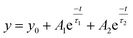
Raman spectroscopy is a potent characterization technique for understanding the vibrational properties of ZnO structures. Raman studies were carried out on both solution samples and the films, using different stabilizers to understand the nucleation and growth of ZnO films. Local vibration modes of ZnO observed in the Raman spectra are shown in Fig. 1.
 |
| | Fig. 1 (a–c) Raman spectra of zinc acetate solutions dissolved in methoxy ethanol using various stabilizers at concentrations (a) 0.05 M (b) 0.1 M and (c) 0.25 M; (d) Raman spectra of ZnO films on Si substrate. | |
Fig. 1a–c show the Raman spectra of zinc acetate dissolved in 2-methoxyethanol. The spectra were acquired using various stabilizers for the three sols with precursor and stabilizer concentrations of 0.05 M, 0.1 M and 0.25 M, respectively, used for the growth of ZnO samples. The results revealed the presence of ZnO and the various chemical entities involved during initial growth, and support the results of two other studies that also reported the formation of ZnO seed crystals in methoxyethanol sols prior to spin-coating and subsequent pyrolysis. The presence of a peak at a wavenumber of 431.1 cm−1 is due to the Zn–O bond with presence of A1 and B2 modes.54 The presence of these modes confirm the nucleation of ZnO in liquid while the amplitudes of A1, B2 and E2 modes suggest homogeneous nucleation to be similar in all the sols studied with the exception of the heated octadecene sol, where it was significantly weaker for all the three concentrations studied. Another interesting observation was that homogeneous nucleation in ethanolamine-based sols became stronger as the concentrations (of precursor and stabilizer) increased while the reverse was true of the oleic acid sol. Raman modes towards higher wave number (800 cm−1 to 1500 cm−1) originate due to C–O, C–H bonds and various carbon entities involved.55 The Raman modes present are indicated in Table 1. The presence of all the mentioned peaks were found for sols of all the three different concentrations used in this study. However, in oleylamine sols and sols containing no stabilizer samples with 0.25 M precursor concentration, a few of the modes disappeared owing to the less stable solutions.
Table 1 Raman modes acquired from zinc acetate, dissolved in methoxyethanol
| Modes present |
Raman shift (cm−1) |
| A1 (TO) |
375 |
| E2 (high) |
431.1 |
| B2 (silent mode) |
540 |
| C–H bond |
832.2 |
| Ethanol |
891.7 |
| (C–C) vibrations, zinc acetate in methoxyethanol |
971.1 |
| (C–O–C) stretching |
1126.6 |
| In plane bending vibrations |
1281 |
| CH3 asymmetric bending due to methoxy |
1455.2 |
Raman studies of ZnO films
Raman studies were also carried out on the solution-deposited films to confirm the presence of the ZnO mode as observed for liquid samples. ZnO is a semiconductor with wurtzite crystal structure that belongs to C46v space group.56 The Raman active phonon modes predicted by group theory are, respectively, A1, E1 and 2E2. Raman spectra of ZnO film is shown in Fig. 1d. The peak at 436 cm−1 is due the presence of E2 (high) mode and corresponds to hexagonal wurtzite phase of ZnO. This is the main ZnO mode that confirms its crystalline nature and phase orientation. A comparison of the main E2 mode of ZnO films with different stabilizers is shown in an inset image of Fig. 1d. Highly intense peaks were seen with oleic acid and oleylamine stabilizers in comparison to other stabilizers. The variation in intensities and broadening of peaks with different stabilizers may be attributed to the variation in crystallinity of ZnO thin films using different stabilizers. A very small shift of ∼2 cm−1 is observed in ZnO film with oleic acid (437.8 cm−1) in comparison to the other stabilizers (436 cm−1). Furthermore, a shift is also seen the ZnO film samples in comparison to liquid ZnO phase, which may be due to the stresses acquired in the ZnO films on Si substrate. No other Raman modes for ZnO were found in the film spectra. Raman modes at around 302 cm−1, 520 cm−1, and 620 cm−1 are due to optic and acoustic modes of silicon substrate.
Effect of sol stabilizer on the morphology and structure of ZnO films
Fig. 2 shows the morphology of ZnO thin films formed using different sol stabilizers. It is evident that the grain sizes of the octadecene and the no-stabilizer films are smaller compared to the other films. Oleic acid and oleylamine stabilizers result in discontinuous films consisting of large aggregates of ZnO film on different parts of the substrate (Fig. 2d and e). The other films are relatively continuous. Triethylamine stabilizer gives a continuous non-porous film with the largest mean grain size of 41.4 nm observed in this study. Fig. 2g shows the films deposited using the ethanolamine stabilizers. Fig. 3a shows the glancing incidence X-ray diffraction (GIXRD) results of the different films. The (100), (101), and (002) peaks are observed in all the diffractograms but the peak intensities are strongest for films formed from oleic acid-stabilized sols and weakest for films made using oleylamine and octadecene.
 |
| | Fig. 2 (a) Schematic illustration of the solution processing technique employed for ZnO film formation; (b–h) SEM images of ZnO films deposited using different sol stabilizers (b) no stabilizer (c) octadecene (d) oleic acid (e) oleylamine (f) triethylamine (g) ethanolamine and (h) triethanolamine. | |
 |
| | Fig. 3 X-ray diffractograms of ZnO films deposited using different stabilizers obtained in (a) glancing angle and (b) powder mode. | |
Perusal of the powder XRD data in Fig. 3b reveals that the acid-stabilized sol–gel ZnO film alone exhibits a nearly exclusive (002) reflection. The dominance of the (002) reflection in the powder X-ray diffractogram of the oleic acid-stabilized ZnO film demonstrates that the crystallites in the film are arranged such that (002) planes are parallel to the substrate plane or the c-axis of the majority of crystallites is oriented perpendicular to the plane of the film. Such a (002) orientation is the preferred orientation for optimal in-plane transport in ZnO thin film transistors.42
Since the preferential orientation of the crystallites is an important factor influencing the electrical behavior of the thin films, it is useful to compare the (002) orientation in films deposited using different stabilizers. In order to compare the preferred orientation for different stabilizers, powder XRD data must be used. Fig. 3b shows the powder XRD data for different stabilizers. The Lotgering factor (LF) is a quantitative measure of crystallographic texture and is given by
| |  | (1) |
where
p is the ratio of the summation of integrated intensities of peaks with preferred orientation to the summation of all peaks in the scanned range in the oriented material, and
p0 is the equivalent value for a randomly oriented material.
57 In addition to texture, information about the size of the crystallites can be obtained from the XRD peak widths, which is useful since crystallite size is known to play a significant role in determining the electrical properties of polycrystalline films. Using the Scherer formula, the crystallite size can be calculated as:
| |  | (2) |
where
K is a constant (equal to 1),
λ is the wavelength of the used X-ray (
λ = 1.54 Å), and
β2θ is subtraction of the instrumental width (0.228°) from the full-width at half maximum of (002) peak.
Table 2 compiles the results and parameters extracted from glancing incidence and powder X-ray diffractograms. As confirmed by the Lotgering factor, in addition to having a large crystallite size, oleic acid produces the highest preferred orientation among the stabilizers. On the other hand, films from oleylamine-stabilized sols are almost randomly oriented with a Lotgering factor of only 0.06. This is surprising since it is usually thought that increasing the pH using alkaline stabilizers and use of higher pH solvents results in a higher
c-axis texture with associated good electrical properties.
46,47 An elaboration of the sol formation process is given in Section S1 in ESI
† while the chemistry of deposition of ZnO films while Section S2 in ESI
† contains a discussion of the reasons behind the variations in ZnO film morphology and structure produced by different stabilizers.
Table 2 Comparison of the (002) peak location, FWHM, crystallite size with XRD and SEM, and crystal orientation using Lotgering factor
| Stabilizer |
Peak location (002) |
FWHM |
Grain size (nm) |
Lotgering Factor (LF) |
SEM grain size (nm) |
| No stabilizer |
34.63 |
0.47 |
39.2 |
0.24 |
27.5 |
| Octadecene |
34.64 |
0.68 |
21 |
0.226 |
20.6 |
| Oleic acid |
34.62 |
0.5 |
34.9 |
0.86 |
33.5 |
| Oleylamine |
34.62 |
0.52 |
32.5 |
0.06 |
31.6 |
| Triethylamine |
34.71 |
0.48 |
37.6 |
0.16 |
41.4 |
| Ethanolamine |
34.79 |
0.49 |
36.2 |
0.138 |
32.3 |
| Triethanolamine |
34.69 |
0.55 |
29.5 |
0.179 |
29.8 |
Optoelectronic properties of ZnO films formed using different stabilizers
Resistivity measurements.
Four point probe measurements were performed on the films to understand their electrical properties, and the results are presented in Table 3. The thickness of the films was measured using ellipsometry. The no-stabilizer and triethanolamine films exhibit the lowest resistivities. Among all the films oleic acid and oleylamine have the highest resistivity values. This is expected since both of these are highly discontinuous. As shown in Table 3, except for ZnO thin films synthesized using oleic acid and oleylamine (which have also poor film continuity), the resistivities of the films are quite low due to high bulk dopant densities. The electron mobilities of the polycrystalline ZnO films also differ depending on the stabilizer used, and we show later in this report that this arises due to the different inter-grain energy barriers for charge transport.
Table 3 Resistivity measurements for ZnO films deposited with different stabilizers
| Stabilizer |
Resistivity (ohm cm) |
Thickness (nm) |
|
Oleic acid and oleylamine films are rough and discontinuous.
|
| No stabilizer |
2.9 |
19 |
| Octadecene |
17.4 |
20 |
| Oleic acid |
138![[thin space (1/6-em)]](https://www.rsc.org/images/entities/char_2009.gif) 070.5 070.5 |
18a |
| Oleylamine |
123191.5 |
16a |
| Triethylamine |
42.5 |
28 |
| Ethanolamine |
169.0 |
40 |
| Triethanolamine |
8.8 |
32 |
We performed Fourier Transform Infrared Spectroscopy (FTIR) found that residual organic complexes were present in the resulting ZnO films. We have included the same in the ESI† of the revised manuscript. As shown in Fig. S4 in ESI,† FTIR peak intensities are similar for all the ZnO films and therefore we conclude that these organic residues contribute equally to the resistivity of the films.
Photoconductivity measurements.
Steady-state and transient photoconductivity measurements were performed on the different ZnO films using bandgap illumination at 254 nm. Fig. 4 shows the dark current and photocurrent for films deposited using each of the different stabilizers.
 |
| | Fig. 4 Comparison of the dark and photocurrent for various stabilizers (a) dark current density (b) photocurrent density. | |
The linear and bias-symmetric I–V relationships in the dark current characteristic in Fig. 5a are indicative of ohmic contacts between the Al electrodes and the ZnO films. Under 254 nm illumination, the measured photocurrents still exhibited roughly linear relationships with applied bias and did not saturate for any of the films, confirming secondary photoconductivity to be operating in these films. The lack of saturation also indicates that the applied lateral electric fields are not sufficient to sweep out all the minority carriers (i.e. holes in our case) before recombination with electrons. Table 4 compares the dark current and photocurrent density values for different stabilizers at 5 V bias voltage. As can be seen, for all the stabilizers the amount of photocurrent is higher than the dark current. However the amount of increase varies for different stabilizers. Ethanolamine and no stabilizer cases show the highest photo-to-dark current ratios (PDR) of 90 and 63 respectively whereas octadecene (PDR of 4.3) and triethylamine (PDR of 4.8) exhibit the lowest ratios. In spite of the simple structure used for the devices, the obtained results for the PDR are in good agreement with the other works available in the literature.29,58 These results are also consistent with the PDR obtained using other deposition methods like MBE59 and CVD.60 It is well-established that the adsorption interactions of the ZnO surface with ambient oxygen play a huge role in the trapping and recombination kinetics during band gap illumination, resulting in the phenomenon of persistent photoconductivity and concomitant very high photoconductive gain.61–64 In the dark, adsorbed oxygen molecules capture free electrons. Hence a depletion region is created near the surface, which degrades the conductivity. This negative depletion region at the surface will also cause an upward band bending at the surface. When films are illuminated with energy higher than the bandgap of ZnO film, electron–hole pairs are generated. The electrons are mobile within the conduction band while the generated holes will travel to the surface due to the band bending and get trapped with the adsorbed oxygen at the surface. Trapping of photogenerated holes at the surface produces desorption of oxygen molecules and also removes the recombination pathway for photogenerated electrons while the high resulting electron concentration in the ZnO film lowers inter-grain energy barriers. Hence, it can be concluded that both the photogenerated electrons and lowering of barrier height contribute to the current increase.29 The differences in the photoresponse of the different stabilizers can be attributed to the different surface states which are related to the different morphologies of the films.29 Hence by affecting the actual surface area of the films (which will affect the number of adsorbed oxygen molecules to the surface of the films), the sol-stabilizers cause the steady state responses of the ZnO films to be different for various stabilizers. Using steady state photoconductivity measurements, the mobility-lifetime product of films deposited using different stabilizers can be calculated.65 The photoconductivity is given as
where
G is the generation rate,
μn(
μp) is the electron (hole) mobility,
τn(
τp) is the lifetime for electrons (holes), and
σph is the photoconductivity which is defined as
Jdiff =
σphE and
Jdiff =
Jon −
Joff where
Jon and
Joff correspond to the current densities when the UV lamp is turned on and off, respectively. Carrier generation (
G) is given as
| |  | (4) |
where
η(=1) is the quantum efficiency,
I0 is the intensity of light at the surface of the film (620 μW cm
−2),
h is the Planck's constant,
ν is the frequency,
R is the reflection coefficient, and
α is the absorption coefficient. Using the values of
α = 120
000 cm
−1 and
R = 0.1 for the wavelength of 254 nm, the generation rate of
G = 8.5 × 10
19 cm
−3 is obtained. The products of mobility-lifetime for ZnO films formed using different stabilizers are shown in
Table 5.
 |
| | Fig. 5 Photoconductivity transients for ZnO films formed using different stabilizers. | |
Table 4 Comparison of dark current and photocurrent density for different stabilizers at 5 V bias
| Stabilizer |
Dark current density (A m−2) |
Photocurrent density (A m−2) |
Photo-to dark current ratio |
| No stabilizer |
1.75 × 10⁴ |
1.1 × 10⁶ |
62.9 |
| Octadecene |
7.2 × 10⁵ |
3.1 × 10⁶ |
4.3 |
| Oleic acid |
3 × 10⁴ |
1.5 × 10⁶ |
50 |
| Oleylamine |
1.1 × 10⁶ |
1.4 × 10⁷ |
13 |
| Triethylamine |
1.3 × 10⁵ |
6.3 × 10⁵ |
4.8 |
| Ethanolamine |
2.1 × 10⁵ |
1.89 × 10⁷ |
90 |
| Triethanolamine |
8.2 × 10³ |
3.3 × 10⁵ |
40 |
Table 5 Mobility-lifetime product for films with different stabilizers
| Stabilizer |
Mobility × lifetime (cm2 V−1) |
| No stabilizer |
1.53 × 10⁻² |
| Octadecene |
3.56 × 10⁻² |
| Oleic acid |
2.18 × 10⁻² |
| Oleylamine |
6.8 × 10⁻² |
| Triethylamine |
7.34 × 10⁻³ |
| Ethanolamine |
2.75 × 10⁻¹ |
| Triethanolamine |
4.8 × 10⁻³ |
Transient photoconductivity was used to extract the decay times for the different ZnO films as shown in Fig. 5. The decay diagram of all the stabilizers was best fitted by a bi-exponential curve as:
| |  | (5) |
The total time constant of the decay is defined as:
| |  | (6) |
The values of the amplitude and time constants for different ZnO films are shown in Table 6.
Table 6 Fitting parameters for decay for different stabilizers
| Stabilizer |
A
1 (A) |
τ
1 (s) |
A
2 (A) |
τ
2 (s) |
τ
total (s) |
Reduced chi-sqr |
Adj R-sqr |
| No stabilizer |
0.76 |
41.7 |
2.2 × 10⁻⁴ |
315.8 |
42.3 |
9.7 × 10⁻¹⁴ |
0.99973 |
| Octadecene |
60.8 |
25.3 |
6.3 × 10⁻⁵ |
235.4 |
25.33 |
3.4 × 10⁻¹⁴ |
0.99846 |
| Oleic acid |
3 × 10⁻⁴ |
276.6 |
1.1 |
39.7 |
40.17 |
7.8 × 10⁻¹⁵ |
0.99924 |
| Oleylamine |
270.1 |
37.7 |
0.001 |
244 |
37.7 |
2.2 × 10⁻¹² |
0.99982 |
| Triethylamine |
5.6 × 10⁻⁴ |
272.8 |
0.73 |
32 |
32.34 |
2.3 × 10⁻¹⁴ |
0.99923 |
| Ethanolamine |
5.7 × 10⁻⁴ |
270 |
4 |
37.8 |
38.03 |
1.9 × 10⁻¹² |
0.99931 |
| Triethanolamine |
0.33 |
33.7 |
3.5 × 10⁻⁵ |
260.3 |
34 |
7.8 × 10⁻¹⁵ |
0.99924 |
As explained before, the adsorbed oxygen at the surface of the ZnO thin films has an important effect on the photoconductive behavior of ZnO thin films. Higher surface area films will have more adsorbed oxygen, which will influence their photoconductive response. Therefore measurement of the surface areas of the films is useful in order to understand the photoconductivity response of ZnO thin films.
EIS measurements.
The surface area and doping of ZnO films were measured using impedance spectroscopy. EIS data was collected in the capacitive regime where blocking behavior is observed. This occurs at potentials more positive, but close to the open circuit potentials, which for the ZnO films were obtained from Tafel plots (shown in Fig. S1, ESI†). Nyquist plots (Fig. S2a in ESI†) show EIS data for ZnO films grown using various stabilizers. The lumped equivalent circuit obtained from the Nyquist plots is shown in Fig. S2b in ESI.† The effective capacitance (Ceff) was calculated in terms of the electrolyte resistance (Rs), constant phase element (CPE) Q1, and n1, which is the exponent of Q1.66 Values of Q1 and n1 were obtained by solving the equivalent circuit model for EIS (Fig. S2a†), which were collected at the potential of −0.2 V (w.r.t. Ag/AgCl). Values of n1 varied between 0.8 and 1, implying capacitive behavior.| |  | (7) |
The actual surface area of ZnO films is given in the equation below, and can be expressed in terms of Ceff, vacuum permittivity (ε0), dielectric constant of zinc oxide (ε), and thickness of the zinc oxide film (L).67
| |  | (8) |
The thickness of each ZnO film was measured with ellipsometry and confirmed with profilometry. For geometrical surface areas of 0.5 × 0.5 cm2, the actual to geometrical surface ratios were calculated and also listed in Table 7.
Table 7 Actual/geometrical surface area and charge carrier concentration (cm−3) measured with EIS for ZnO thin films of various stabilizers
| Stabilizer type |
Actual/geometrical surface area |
Charge carrier concentration [cm−3] |
| Oleylamine |
3.75 |
6.26 × 10¹⁶ |
| Oleic acid |
5.00 |
2.10 × 10¹⁷ |
| Ethanolamine |
13.8 |
4.7 × 10¹⁸ |
| Octadecene |
2 |
3.5 × 10¹⁶ |
| Triethylamine |
4.67 |
7.05 × 10¹⁶ |
| Triethanolamine |
8.4 |
7 × 10¹⁶ |
| No stabilizer |
6.50 |
9.40 × 10¹⁶ |
These actual to geometrical surface area ratios are qualitatively consistent with surface roughness of the films, shown in Fig. 2 and are factored into capacitance values that were extracted from impedance versus potential data, in order to plot the Mott Schottky's plots (shown in Fig. S2c in ESI†). Comparing the surface area of the continuous films with the tabulated values of the photo-to-dark current ratio (Table 4), it is observed that excluding the no stabilizer case, films with a higher surface area also exhibit a higher PDR and a higher photoconductive decay lifetime (Table 5). This is consistent with stated mechanism of hole trapping by surface adsorbed oxygen species, which in turn increases the photoconductive gain and photoconductive decay lifetime by removing recombination pathways for electrons. As for the no stabilizer case, we surmise that the high PDR and relatively long decay lifetime result from a high density of impurities (acting as color centers) in addition to surface traps since nucleation and growth of the ZnO films occurred without the presence of coordinating ligands save the solvent itself. For the discontinuous films (oleylamine and oleic acid) we observe a different behavior. For instance triethylamine has a higher surface ratio compared to oleylamine. However oleylamine shows a higher PDR. The same behavior is observed for triethanolamine and oleic acid. As mentioned before, oleic acid and oleylamine are rough discontinuous films, which makes the measurement of film thickness very difficult. This will lead to errors in calculating the surface area, which causes deviations from the proposed behavior. Table S1 in ESI† ranks the different ZnO films on the basis of their surface area and shows that excepting the no stabilizer case and the discontinuous films discussed above, the trends in PDR and lifetime follow the surface area of the films.
Thin film transistor measurements.
In order to obtain a better understanding of the electrical properties of the ZnO thin films, TFTs with different stabilizers were fabricated. Fig. 6 shows the ID–VDS and ID–VGS curves of the different stabilizer TFTs.
 |
| | Fig. 6 Operating characteristics (ID–VDS) and (insets) transfer characteristics (ID–VGS) of the TFTs fabricated from ZnO thin films formed using different stabilizers. | |
As can be seen from the ID–VDS curves, the oleic acid and oleylamine stabilized ZnO films do not show saturation behavior. The other devices exhibit different saturation levels (hard vs. soft saturation). Hard saturation is the flatness of the variation of the drain current (ID) for large drain bias (VDS) and occurs when the entire thickness of the ZnO channel is depleted of free electrons in the drain contact. Devices showing hard saturation have a higher output impedance which is a desirable feature for transistors in circuit applications.68 Due to the increase of free electrons in the transistor channel at higher positive gate voltages, achieving hard saturation at higher gate voltages is challenging. As can be seen from the ID–VDS curves, the TFTs fabricated without stabilizer and with triethylamine stabilizer operate in hard saturation at high gate voltages. As for octadecene and triethanolamine, at high gate voltages soft saturation behavior while hard saturation is observed at low gate voltages. Further analysis was performed to measure the saturation mobility, threshold voltage and effective mobility. The drain current of the TFT in saturation regime is given by
| |  | (9) |
Using the slope of the  curve and the intersection of this curve with the x-axis, the saturation mobility and threshold voltage were respectively calculated. The electron saturation field-effect mobility (μsat) is insensitive to threshold voltage and is less dependent on the contact resistance. However it describes the pinched-off model where the effective channel length (Leff) of the device is smaller than the actual channel.69 The polycrystalline nature of ZnO films causes a large number of electron traps to be formed at grain boundaries. Application of a positive gate voltage produces trap filling, thus enhancing the electrical performance of the device. This is not accounted for in the saturation mobility. In order to separate out the effect of gate voltage on the mobility, a parameter known as the effective mobility is used which is defined at low drain voltage as follows:
| |  | (10) |
The effective mobility (μeff) takes the variation of mobility due to gate voltage into account. However the threshold voltage must be known and μeff shows a higher sensitivity to contact resistance compared to μsat.69 In order to overcome the issue of the dependence of effective mobility on the threshold voltage, the field effect mobility (also known as the mobility in the linear region of the operating characteristic) is defined as (at low drain voltage) follows:
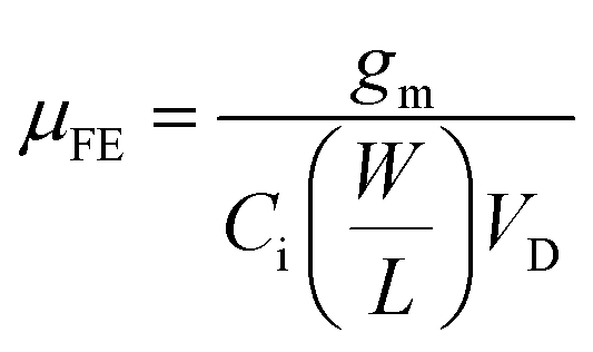
| |  | (11) |
Due to the high dopant density, bulk conduction forms an alternate path for charge transport from source to drain in addition to the channel. Hence the device exhibits a bulk depletion mode regime in addition to the channel accumulation and depletion regimes (similar to gated resistor-type FETs).70 A clear transition from accumulation to bulk conduction in the form of a plateau region is seen for nearly all the stabilizers used in the ID–VGS plots (insets in Fig. 6). This bulk current contributes to the leakage current in the off-state of the transistors. The ID–VDS and ID–VGS characteristics of such bulk depletion transistors can be used to obtain a wealth of detail regarding the bulk properties of the ZnO. The saturation mobility, effective mobility, field effect mobility, and threshold voltage values for different stabilizers are shown in Table 8.
Table 8 Extracted parameters from the ID–VDS and ID–VGS curves of TFTs (W = 40 μm, L = 20 μm)
|
Doping values of oleic acid and oleylamine unreliable due to discontinuity of the films.
|
| Stabilizer |
Triethylamine |
Triethanolamine |
Octadecene |
No stabilizer |
Oleic acid |
Oleylamine |
Ethanolamine |
| Saturation mobility (cm2 V−1 s−1) |
0.15 |
0.4 |
0.12 |
0.02 |
N/A |
N/A |
0.6 |
| Effective mobility (cm2 V−1 s−1) |
0.25 |
0.7 |
0.08 |
0.11 |
N/A |
N/A |
0.87 |
| Threshold voltage Vth (V) |
1.9 |
8.7 |
14.8 |
9.0 |
N/A |
N/A |
−9.1 |
| Field effect mobility (cm2 V−1 s−1) |
0.33 |
1.7 |
0.29 |
0.05 |
0.007 |
0.00002 |
2.0 |
| Dopant density Nd (cm−3) |
7.1 × 10¹⁶ |
7 × 10¹⁶ |
3.5 × 10¹⁶ |
9.4 × 10¹⁶ |
2.1 × 10¹⁷a |
6.3 × 10¹⁶a |
4.7 × 10¹⁸ |
| Bulk mobility (cm2 V−1 s−1) |
2.1 |
10 |
11 |
23 |
2.1 × 10⁻⁴ |
8.1 × 10⁻⁴ |
7.8 × 10⁻³ |
| Inter-grain activation barrier Vb (V) |
0.23 |
0.19 |
0.22 |
0.28 |
0.33 |
0.46 |
0.17 |
| Trap density Nt (cm−2) |
8.0 × 10¹¹ |
7.3 × 10¹¹ |
5.5 × 10¹¹ |
1012 |
1.6 × 10¹² |
1.1 × 10¹² |
5.6 × 10¹² |
As can be seen from the devices, the linear region field effect mobility is surprisingly higher than saturation mobility. This is due to the fact that the saturation mobility, unlike the field effect mobility, ignores the effect of gate voltage. At higher gate voltages, charge carriers fill the traps at the interface hence improving the mobility of the device. The field effect and effective mobility values were measured at VGS = 80 V. This high voltage value resulted in filling of traps by carriers, which caused the field effect mobility to be higher than saturation mobility. Ethanolamine, triethanolamine, and triethylamine are stabilizers that show higher mobility values. On the other hand, the discontinuity in oleic acid and oleylamine stabilized ZnO films results in lower mobility values compared to other films. The main limiting factor(s) in charge transport in polycrystalline ZnO films are the grain boundaries. Hence characterizing the grain boundaries can lead to a better understanding of the charge transport in the ZnO films of different stabilizers. Hossain et al. developed a model for polycrystalline ZnO thin film transistors. In this model it is assumed that all the defects are segregated in the grain boundaries. Each grain boundary is modeled as a double Schottky barrier. The height of the barrier is a function of defect density and gate voltage. Based on this model the grain boundary barrier height can be extracted from the field effect mobility using:71
where
μFE is the field effect mobility,
L is the channel length,
Vb is the barrier height,
ng is the number of grain boundaries in the channel length,
k is the Boltzmann constant and

(
A = 32 A K
−2 cm
−2 is Richardson's constant,

). The grain height barrier heights (
Vb) are seen in
Table 8. Hence among all the stabilizers ethanolamine and oleylamine have the lowest and highest grain boundary barriers, respectively. Oleic acid has a relatively larger barrier height compared to the remaining stabilizers. The density of the trapped charge density at the grain boundary is calculated as follows:
71
The values of the trapped charge density at VGS = 80 V is calculated in Table 8. As can be seen from the values, triethanolamine and ethanolamine have the lowest and highest values of the trapped charge density in the grain boundaries, respectively. The values of the trap density in the ZnO films formed from the various stabilizers are in the same range and are in agreement with the other reports.72
Conclusions
We investigated the effect of six sol stabilizers on the morphology and electrical performance of ZnO thin films. The stabilizers not only included short chain alkanolamines typically used in the solution deposition of ZnO thin films but also examined longer chain, high boiling point coordinating agents commonly used in II–VI quantum dot synthesis such as oleylamine, oleic acid and octadecene. Sols stabilized using oleic acid resulted in a very strong (002) texture in ZnO thin films. However due to the discontinuity of the film the electrical performance of these films was poor. Using steady state photoconductivity measurements, the photoconductivity of the films deposited using various stabilizers were studied. Films deposited using different stabilizers exhibited different photo to dark current ratio. This is attributed to different amount of oxygen molecules adsorbed to the surface of the films. Films like ethanolamine, which have a higher surface area, adsorb a larger number of oxygen molecules and hence show a higher photo to dark current ratio. The sum of the mobility-lifetime product of electrons and holes was measured for different films by transient photoconductivity measurement. Thin film transistors were fabricated and different parameters like mobility and threshold voltage was measured for each TFT. Using impedance spectroscopy the doping value of each ZnO film was calculated. Using the extracted field effect mobility from the TFT characteristics and doping values from the impedance spectroscopy the approximate value of the trapped charge density at grain boundaries is calculated.
In polycrystalline ZnO thin films, grain boundaries are the main factor in limiting the charge transport. Hence, characterizing these grain boundaries could lead to a better understanding about the effect of grain boundaries in limiting the charge transport. Using the field effect mobility extracted from the TFT curves and the doping value of the thin films extracted from the C–V measurements, the barrier height of grain boundaries and the trapped charge density in these grain boundaries was calculated and compared.
Materials
Zinc acetate dihydrate (ZAC, Fisher Scientific) was the salt used for deposition of ZnO thin films. The sol stabilizers used were as follows: oleic acid (Fisher Scientific, 97%), triethylamine (Sigma-Aldrich, 99%), triethanolamine (Fisher Scientific, 97%), ethanolamine (Acros Organics, 99%), octadecene (Acros Organics, 90%) and oleylamine (Acros Organics, C18 content 80–90%). 2-Methoxyethanol (Sigma-Aldrich, 99%) was the solvent used.
Device fabrication
The Si–SiO2 substrates were cleaned in piranha (H2SO4/H2O2 3:1) solution for 20 minutes. Three sols of 0.05 M, 0.1 M, and 0.25 M were prepared for each of the stabilizers while maintaining the ratio of [stabilizer]/[Zn2+] at 1. For octadecene and oleic acid as stabilizers and also when no stabilizer was used, the sols were turbid due to insufficient solubility of the precursor in methoxyethanol. These sols were heated while stirring until fully transparent while triethanolamine, triethylamine, ethanolamine, and oleylamine solutions required no heating to form clear, homogeneous solutions. The solutions were spin-coated on to 250 nm thermal oxide-coated Si substrates at 1000 rpm for 60 s and dried and annealed at 120 °C and 500 °C respectively as depicted in Fig. 2a. For each stabilizer, deposition from solution was performed from lowest to highest concentration (0.05 M to 0.25 M) in sequential order in order to separate the seeding, coarsening and aggregation stages as much as possible. The Al electrodes were deposited using magnetron sputtering after one step lithography followed by lift-off. The size of electrodes and fabricated devices were 100 μm × 80 μm and 500 μm × 100 μm, respectively.
Instrumentation
The morphologies of the ZnO thin films were imaged using a Hitachi S-4800 field emission scanning electron microscope (FESEM). The X-ray diffraction data was collected in glancing angle mode as well as powder mode by a Bruker D8 Discover system. Raman spectroscopic studies were carried out on both liquid samples (i.e. sols used to deposit ZnO) and films in back scattering mode using Nicolet Almega XR Raman Microscope. Micro-Raman imaging using a 532 nm laser excitation source and a beam spot size of 2 μm was used to record the Raman spectra from the samples. Micro-Raman studies were carried out on the sols. Resistivity measurements were performed using a four-point probe (Lucus Pro 4 4000). Electrical characteristics of the fabricated field-effect transistors were measured in a probe station (creative devices) using a Keithley 4200 semiconductor parameter analyzer. For steady-state and transient photoconductivity measurements, 254 nm illumination from a Spectroline E-series UV lamp was used as the excitation source while the electrical characteristics were measured by the Keithley-4200 mentioned above. Electrochemical impedance spectroscopy (EIS) and impedance versus potential data were collected in a three-electrode electrochemical cell with a Ag/AgCl reference electrode, by using a CHI 600D potentiostat (CH Instruments Inc.). All electrochemical measurements used a 0.1 M KCl solution electrolyte at room temperature. Samples were prepared by wrapping parafilm all around except for a 0.5 cm × 0.5 cm area exposed to the electrolyte.
Acknowledgements
This project was funded through grants from the National Research Council of Canada (NRC). S. F. thanks Alberta Innovates Technology Futures for scholarship support. Device fabrication and testing used research infrastructure made possible by a Leaders Opportunity Fund grant to K. S. from the Canada Foundation for Innovation (CFI) with matching funds from the Alberta Small Equipment Grants Program (SEGP). We thank the Canadian Microelectronics Consortium and NRC National Institute for Nanotechnology (NINT) for supporting equipment use. Staff assistance at the UofA NanoFab and NRC-NINT is acknowledged. We also thank Mourad Benlamri for assistance with resistivity measurements.
References
- S. B. Herner, A. Bandyopadhyay, S. V. Dunton, V. Eckert, J. Gu, K. J. Hsia, S. Hu, C. Jahn, D. Kidwell, M. Konevecki, M. Mahajani, K. Park, C. Petti, S. R. Radigan, U. Raghuram, J. Vienna and M. A. Vyvoda, IEEE Electron Device Lett., 2004, 25, 271–273 CrossRef CAS.
- Z. Lisong, J. Soyoun, E. Brandon and T. N. Jackson, IEEE Trans. Electron Devices, 2006, 53, 380–385 CrossRef.
- L. Maiolo, A. Pecora, F. Maita, A. Minotti, E. Zampetti, S. Pantalei, A. Macagnano, A. Bearzotti, D. Ricci and G. Fortunato, Sens. Actuators, B, 2013, 179, 114–124 CrossRef CAS.
- M. A. Marrs, E. J. Bawolek, B. P. O'Brien, J. T. Smith, M. Strnad and D. C. Morton, SID Int. Symp. Dig. Tech. Pap., 2013, 44, 455–457 CrossRef CAS.
- A. Nathan, B.-k. Park, Q. Ma, A. Sazonov and J. A. Rowlands, Microelectron. Reliab., 2002, 42, 735–746 CrossRef.
- N. Young, G. Harkin, R. Bunn, D. McCulloch, R. Wilks and A. Knapp, IEEE Electron Device Lett., 1997, 18, 19–20 CrossRef.
-
M. Zhiguo, C. Haiying, Q. Chengfeng, W. Liduo, H. S. Kwok and W. Man, 2000.
- S. Tatsuo, Jpn. J. Appl. Phys., 2004, 43, 3257 CrossRef.
- Y.-H. Tai, K. Yan-Fu and L. Yun-Hsiang, IEEE Trans. Electron Devices, 2009, 56, 50–56 CrossRef CAS.
- F. V. Farmakis, J. Brini, G. Kamarinos and C. A. Dimitriadis, IEEE Electron Device Lett., 2001, 22, 74–76 CrossRef CAS.
-
G. Scarpa, A. L. Idzko, A. Munzer and S. Thalhammer, Ieee, Low-Cost Solution-Processable Organic Thin-Film Transistors for (bio)Sensing Applications, 2011 Search PubMed.
- N. A. Azarova, J. W. Owen, C. A. McLellan, M. A. Grimminger, E. K. Chapman, J. E. Anthony and O. D. Jurchescu, Org. Electron., 2010, 11, 1960–1965 CrossRef CAS.
- A. T. Zocco, H. You, J. A. Hagen and A. J. Steckl, Nanotechnology, 2014, 25, 094005 CrossRef PubMed.
- M. H. Choi, B. S. Kim and J. Jang, IEEE Electron Device Lett., 2012, 33, 1571–1573 CrossRef CAS.
- K. Fukuda, Y. Takeda, M. Mizukami, D. Kumaki and S. Tokito, Sci. Rep., 2014, 4, 3947 Search PubMed.
- K. H. Lee, K. Lee, M. S. Oh, J. M. Choi, S. Im, S. Jang and E. Kim, Org. Electron., 2009, 10, 194–198 CrossRef CAS.
- C. Santato, I. Manunza, A. Bonfiglio, F. Cicoira, P. Cosseddu, R. Zamboni and M. Muccini, Appl. Phys. Lett., 2005, 86, 141106 CrossRef.
- Y. G. Ha, S. Jeong, J. S. Wu, M. G. Kim, V. P. Dravid, A. Facchetti and T. J. Marks, J. Am. Chem. Soc., 2010, 132, 17426–17434 CrossRef CAS PubMed.
- X. G. Yu, N. J. Zhou, S. J. Han, H. Lin, D. B. Buchholz, J. S. Yu, R. P. H. Chang, T. J. Marks and A. Facchetti, J. Mater. Chem. C, 2013, 1, 6532–6535 RSC.
- M. A. McCarthy, B. Liu, E. P. Donoghue, I. Kravchenko, D. Y. Kim, F. So and A. G. Rinzler, Science, 2011, 332, 570–573 CrossRef CAS PubMed.
- H. C. Chang, C. L. Liu and W. C. Chen, ACS Appl. Mater. Interfaces, 2013, 5, 13180–13187 CAS.
- B. Kumar, B. K. Kaushik and Y. S. Negi, J. Mater. Sci.: Mater. Electron., 2014, 25, 1–30 CrossRef CAS.
- U. Ozgur, Y. I. Alivov, C. Liu, A. Teke, M. A. Reshchikov, S. Dogan, V. Avrutin, S. J. Cho and H. Morkoc, J. Appl. Phys., 2005, 98, 041301 CrossRef.
- Z. Brankovic, G. Brankovic, D. Poleti and J. A. Varela, Ceram. Int., 2001, 27, 115–122 CrossRef CAS.
- Y. Q. Fu, J. K. Luo, X. Y. Du, A. J. Flewitt, Y. Li, G. H. Markx, A. J. Walton and W. I. Milne, Sens. Actuators, B, 2010, 143, 606–619 CrossRef CAS.
- Q. Wan, Q. H. Li, Y. J. Chen, T. H. Wang, X. L. He, J. P. Li and C. L. Lin, Appl. Phys. Lett., 2004, 84, 3654–3656 CrossRef CAS.
- T. Aeugle, H. Bialas, K. Heneka and W. Pleyer, Thin Solid Films, 1991, 201, 293–304 CrossRef CAS.
- S. A. Studenikin, N. Golego and M. Cocivera, J. Appl. Phys., 2000, 87, 2413–2421 CrossRef CAS.
- T. Ghosh and D. Basak, Nanotechnology, 2010, 21, 375202 CrossRef CAS PubMed.
- M. Benlamri, K. M. Bothe, A. M. Ma, G. Shoute, A. Afshar, H. Sharma, A. Mohammadpour, M. Gupta, K. C. Cadien, Y. Y. Tsui, K. Shankar and D. W. Barlage, Phys. Status Solidi RRL, 2014, 9999 Search PubMed , n/a-n/a.
- C. S. Li, Y. N. Li, Y. L. Wu, B. S. Ong and R. O. Loutfy, J. Appl. Phys., 2007, 102, 076101 CrossRef.
- H. Bahadur, A. K. Srivastava, R. K. Sharma and S. Chandra, Nanoscale Res. Lett., 2007, 2, 469–475 CrossRef CAS.
- A. Chatterjee, C. H. Shen, A. Ganguly, L. C. Chen, C. W. Hsu, J. Y. Hwang and K. H. Chen, Chem. Phys. Lett., 2004, 391, 278–282 CrossRef CAS.
- M. Toyoda, J. Watanabe and T. Matsumiya, J. Sol-Gel Sci. Technol., 1999, 16, 93–99 CrossRef CAS.
- J. G. Quiñones-Galván, I. M. Sandoval-Jiménez, H. Tototzintle-Huitle, L. A. Hernández-Hernández, F. de Moure-Flores, A. Hernández-Hernández, E. Campos-González, A. Guillén-Cervantes, O. Zelaya-Angel and J. J. Araiza-Ibarra, Results Phys., 2013, 3, 248–253 CrossRef.
- S. Yamabi and H. Imai, J. Mater. Chem., 2002, 12, 3773–3778 RSC.
- M. Izaki and J. Katayama, J. Electrochem. Soc., 2000, 147, 210–213 CrossRef CAS.
- L. Vayssieres, K. Keis, S. E. Lindquist and A. Hagfeldt, J. Phys. Chem. B, 2001, 105, 3350–3352 CrossRef CAS.
- K. Ito and K. Nakamura, Thin Solid Films, 1996, 286, 35–36 CrossRef CAS.
- D. Raviendra and J. K. Sharma, J. Appl. Phys., 1985, 58, 838–844 CrossRef CAS.
- P. Obrien, T. Saeed and J. Knowles, J. Mater. Chem., 1996, 6, 1135–1139 RSC.
- C. S. Li, Y. N. Li, Y. L. Wu, B. S. Ong and R. O. Loutfy, J. Mater. Chem., 2009, 19, 1626–1634 RSC.
- L. Znaidi, Mater. Sci. Eng., B, 2010, 174, 18–30 CrossRef CAS.
- G. Adamopoulos, A. Bashir, S. Thomas, W. P. Gillin, S. Georgakopoulos, M. Shkunov, M. A. Baklar, N. Stingelin, R. C. Maher, L. F. Cohen, D. D. C. Bradley and T. D. Anthopoulos, Adv. Mater., 2010, 22, 4764–4769 CrossRef CAS PubMed.
- A. H. Adl, A. Ma, M. Gupta, M. Benlamri, Y. Y. Tsui, D. W. Barlage and K. Shankar, ACS Appl. Mater. Interfaces, 2012, 4, 1423–1428 CAS.
- T. Jun, Y. Jung, K. Song and J. Moon, ACS Appl. Mater. Interfaces, 2011, 3, 774–781 CAS.
- P. Sagar, P. K. Shishodia and R. M. Mehra, Appl. Surf. Sci., 2007, 253, 5419–5424 CrossRef CAS.
- S. Benramache, A. Rahal and B. Benhaoua, Optik, 2014, 125, 663–666 CrossRef CAS.
- Y. Liao, X. L. Zhou, X. W. Xie and Q. X. Yu, J. Mater. Sci.: Mater. Electron., 2013, 24, 4427–4432 CrossRef CAS.
- S. Chakrabarti, D. Ganguli and S. Chaudhuri, Mater. Lett., 2004, 58, 3952–3957 CrossRef CAS.
- M. Ohyama, H. Kozuka, T. Yoko and S. Sakka, J. Ceram. Soc. Jpn., 1996, 104, 296–300 CrossRef CAS.
- K. Govender, D. S. Boyle, P. B. Kenway and P. O'Brien, J. Mater. Chem., 2004, 14, 2575–2591 RSC.
- P. H. Vajargah, H. Abdizadeh, R. Ebrahimifard and M. Golobostanfard, Appl. Surf. Sci., 2013, 285, 732–743 CrossRef.
- S. B. Yahia, L. Znaidi, A. Kanaev and J. P. Petitet, Spectrochim. Acta, Part A, 2008, 71, 1234–1238 CrossRef PubMed.
- M. M. Yang, D. A. Crerar and D. E. Irish, Geochim. Cosmochim. Acta, 1989, 53, 319–326 CrossRef CAS.
- K. A. Alim, V. A. Fonoberov, M. Shamsa and A. A. Balandin, J. Appl. Phys., 2005, 97, 124313 CrossRef.
- R. Furushima, S. Tanaka, Z. Kato and K. Uematsu, J. Ceram. Soc. Jpn., 2010, 118, 921–926 CrossRef CAS.
- K. L. Foo, M. Kashif, U. Hashim and M. E. Ali, Optik, 2013, 124, 5373–5376 CrossRef CAS.
- Y. W. Heo, D. P. Norton and S. J. Pearton, J. Appl. Phys., 2005, 98, 073502 CrossRef.
- H. C. Hsu, C. S. Cheng, C. C. Chang, S. Yang, C. S. Chang and W. F. Hsieh, Nanotechnology, 2005, 16, 297–301 CrossRef CAS PubMed.
- T. Yasutaka, K. Masaaki, K. Akiko, M. Hideki and O. Yutaka, Jpn. J. Appl. Phys., 1994, 33, 6611 CrossRef.
- S. A. Studenikin, N. Golego and M. Cocivera, J. Appl. Phys., 1998, 84, 5001–5004 CrossRef CAS.
- C. Soci, A. Zhang, B. Xiang, S. A. Dayeh, D. P. R. Aplin, J. Park, X. Y. Bao, Y. H. Lo and D. Wang, Nano Lett., 2007, 7, 1003–1009 CrossRef CAS PubMed.
- Y. Jin, J. Wang, B. Sun, J. C. Blakesley and N. C. Greenham, Nano Lett., 2008, 8, 1649–1653 CrossRef CAS PubMed.
- K. W. Liu, J. G. Ma, J. Y. Zhang, Y. M. Lu, D. Y. Jiang, B. H. Li, D. X. Zhao, Z. Z. Zhang, B. Yao and D. Z. Shen, Solid-State Electron., 2007, 51, 757–761 CrossRef CAS.
- B. Hirschorn, M. E. Orazem, B. Tribollet, V. Vivier, I. Frateur and M. Musiani, Electrochim. Acta, 2010, 55, 6218–6227 CrossRef CAS.
- D. J. Blackwood, Electrochim. Acta, 2000, 46, 563–569 CrossRef CAS.
- R. L. Hoffman, B. J. Norris and J. F. Wager, Appl. Phys. Lett., 2003, 82, 733–735 CrossRef CAS.
- E. Fortunato, P. Barquinha and R. Martins, Adv. Mater., 2012, 24, 2945–2986 CrossRef CAS PubMed.
- J.-P. Colinge, C.-W. Lee, A. Afzalian, N. D. Akhavan, R. Yan, I. Ferain, P. Razavi, B. O'Neill, A. Blake, M. White, A.-M. Kelleher, B. McCarthy and R. Murphy, Nat. Nanotechnol., 2010, 5, 225–229 CrossRef CAS PubMed.
- F. M. Hossain, J. Nishii, S. Takagi, A. Ohtomo, T. Fukumura, H. Fujioka, H. Ohno, H. Koinuma and M. Kawasaki, J. Appl. Phys., 2003, 94, 7768–7777 CrossRef CAS.
- P. F. Carcia, R. S. McLean, M. H. Reilly and G. Nunes, Appl. Phys. Lett., 2003, 82, 1117–1119 CrossRef CAS.
Footnote |
| † Electronic supplementary information (ESI) available. See DOI: 10.1039/c5ra18642k |
|
| This journal is © The Royal Society of Chemistry 2015 |
Click here to see how this site uses Cookies. View our privacy policy here. 
 Open Access Article
 This Open Access Article is licensed under a Creative Commons Attribution-Non Commercial 3.0 Unported Licence
 a and
Karthik
Shankar
*ab
a and
Karthik
Shankar
*ab


 curve and the intersection of this curve with the x-axis, the saturation mobility and threshold voltage were respectively calculated. The electron saturation field-effect mobility (μsat) is insensitive to threshold voltage and is less dependent on the contact resistance. However it describes the pinched-off model where the effective channel length (Leff) of the device is smaller than the actual channel.69 The polycrystalline nature of ZnO films causes a large number of electron traps to be formed at grain boundaries. Application of a positive gate voltage produces trap filling, thus enhancing the electrical performance of the device. This is not accounted for in the saturation mobility. In order to separate out the effect of gate voltage on the mobility, a parameter known as the effective mobility is used which is defined at low drain voltage as follows:

 (A = 32 A K−2 cm−2 is Richardson's constant,
  ). The grain height barrier heights (Vb) are seen in Table 8. Hence among all the stabilizers ethanolamine and oleylamine have the lowest and highest grain boundary barriers, respectively. Oleic acid has a relatively larger barrier height compared to the remaining stabilizers. The density of the trapped charge density at the grain boundary is calculated as follows:71