
A simple and room temperature sol–gel process for the fabrication of cobalt nanoparticles as an effective catalyst for carbon nanotube growth
Nor Najihah Zulkapli,
Mohd Asyadi Azam*,
Nik Mohamad Azren Mohd Zubir,
Nur Azura Ithnin and
Mohd Warikh Abd Rashid
Carbon Research Technology Research Group, Faculty of Manufacturing Engineering, Universiti Teknikal Malaysia Melaka, Hang Tuah Jaya, 76100 Durian Tunggal, Melaka, Malaysia. E-mail: asyadi@utem.edu.my
First published on 27th October 2015
Abstract
Cobalt catalyst thin films were prepared on silicon wafers using a spin coating process. The detailed structural characteristics of the cobalt films/particles and synthesized carbon nanotubes were studied using X-ray analysis, high resolution electron microscopy, and Raman spectroscopy. The thickness of the catalyst thin films can be controlled by controlling the spin coating parameter, and the thickness of the films can be reduced by increasing the spin speed. Cobalt catalyst particles can be achieved by post-heat treatment within the range of 450–600 °C. However, increasing the post-heat treatment temperature may lead to larger particle formation. The optimum values of thin film thickness and particle size were 12.1 nm at 8000 rpm and 10.6 nm at 450 °C, respecively. The study also demonstrated that single-walled carbon nanotubes could be grown from cobalt catalyst particles via catalytic chemical vapor deposition of ethanol.
Introduction
The development of nanotechnology has led to growth in the use of carbon nanotubes (CNTs). This development has led to the large potential for the usage of CNTs in the electrical industry, such as for photovoltaics, sensors, semiconductor devices, displays, and conductors.1,2 Catalyst nanoparticles are essential for growing CNTs. These catalyst nanoparticles can be obtained from thin films after a heat treatment process. However, controlling catalyst formation can improve CNT growth. The thin films consist of a thin layer of resistor material deposited on the surface of a substrate, followed by a thin layer of metal. The thin films are formed mostly through deposition, either by a physical or chemical method.3,4 Transition metals, such as iron, cobalt, and nickel, are reported to be the most effective catalysts to grow CNTs because of their high carbon solubilities at high temperatures and high diffusion rates.5 Among these three potential transition metals for CNT growth, Co is selected as the catalyst because it can produce good quality CNTs and it is the most reactive catalyst for an ethanol-based chemical vapor deposition (CVD) system.6,7In CNT production, a physical vapor deposition (PVD) method is widely used to produce a thin film, which is a layer that contains the catalyst nanoparticles. These catalysts are important in CNT growth through alcohol catalytic CVD (ACCVD). PVD is commonly used for industrial scale catalyst film production; this technique is suitable for obtaining uniform thin film and controlling its thickness. However, the ratio of the deposited material after deposition is less than 10% of the source material. The accumulated material is then scraped off using a photolithographic method. Thus, about 99% of the expensive high technology material is wasted; moreover, the coating rate is slow. The machine needs a high vacuum system and a large cooling system to evacuate the air inside the chamber and cool down the system during the deposition process, respectively. Therefore, a solution process, specifically spin coating, is a promising technique to produce uniform, ultrathin film with the thickness of a nanometer.8 Furthermore, solution process techniques have been given high levels of attention because of the simple deposition procedures, ease of control of the chemical components, and being low cost preparation methods to obtain high quality thin films.9
ACCVD is the most reliable technique for CNT growth because of its wide substrate selectivity, good economic value, and high catalytic reactivity.10–12 The CNTs grown using this technique have high potential for use in electronic device fabrication due to reduced formation of amorphous carbon and CNTs are produced with high purities.13,14 The properties and qualities of the CNTs can also be determined at the beginning of the catalyst preparation. The most suitable catalyst for the ACCVD technique is a cobalt catalyst.6 Previously it was shown that, through decomposition in air, the oxide layer will be a Co3O4 phase while under vacuum, Co and CoO phases could be found.15 Hence, this report presents an analysis and extensive study on the effect of the spin coating speed and heat treatment temperatures in the catalyst preparation. Subsequently, the CNT growth performance using the ACCVD technique of the sample with the optimum parameters was measured.
Experimental
Nanosized Co thin films were synthesized by using a sol gel spin-coated technique. The precursor solution was prepared by diluting 42 mg of Co acetate tetrahydrate, Co(CH3COOCH)2·4H2O, in 10 mL of absolute ethanol to produce a solution with a concentration of 16.8 mmol L−1.16 The solution was stirred vigorously for 10 min and left for 2 h, thereby leading to the formation of a light pink colored solution.16 A p-type silicon wafer was cut into 15 mm × 15 mm sizes. The substrates were soaked in acetone, left for a 10 min sonication in ethanol, and dried by using nitrogen gas.The precursor solution of Co acetate tetrahydrate/absolute ethanol was spin coated on the cleaned substrates at 6500, 7000, 7500, and 8000 rpm for 60 s. Subsequently, the spin-coated wafers were pre-heated at 250 °C for 1 min to vaporize the solvent, thus leaving Co catalyst thin films on the wafers. Later, the pre-heated wafers were placed in a vacuum furnace for a heat treatment process at 450, 500, 550, and 600 °C to obtain Co catalyst nanoparticles.
The prepared catalyst thin film was placed in a quartz tube in a furnace for the CNT growth process. The tube was evacuated using an oil-free scroll pump at 0.4 Pa. To prevent the oxidation of the Co catalyst, Ar gas was injected into the system at a pressure of 400 Pa concurrently with 5 min of rapid heating and a 5 min annealing process. Once the annealing process was completed, the Ar gas flow was quickly stopped, and ethanol vapor was immediately introduced into the system at flow rates of 100–150 sccm. The growth process was fixed at 2.0 kPa and 15 min internal pressure and CVD processing time, respectively. After the growth process, the ethanol gas flow was stopped, and the samples were left to cool to room temperature. The growth process was repeated for CVD processing temperatures of 650, 675, 700, 725, and 750 °C.
The surface morphology of the sample was characterized by using a field emission scanning electron microscope (FESEM, Hitachi SU8100) operated at 5 kV. The optimum parameters can be determined from the smallest and most uniform thickness of the Co catalyst thin film by using FESEM. The individual CNT structure and Co nanoparticles were also characterized using a high-resolution transmission electron microscopy (HRTEM) system. TEM samples for Co on SiO2/Si were prepared using a focused ion beam (FIB) technique, and the CNT samples were prepared using a sonication technique. Surface chemical state analysis was conducted using X-ray photoelectron spectroscopy (XPS, Fison Instruments S-PROBE ESCA) with Al Kα (1486.6 eV) as the X-ray source. The samples were analyzed at a 90° take-off angle to the surface. A C 1s narrow spectrum, at 284.8 eV with a chamber pressure during the measurement of 10−7 Pa, was used to calibrate the photoelectron binding energy (BE). The crystal structures of the cobalt oxide thin films were characterized using a X-ray diffractometer using Cu Kα radiation in the 2theta range of 10–90° with a wavelength of 1.5406 Å. Raman analysis was performed through Raman spectroscopy (Uni-RAM 3500) with a laser excitation of 532 nm wavelength (Nd:YAG).17
Results and discussion
Morphological analysis of the Co catalysts
Spin speed is the most crucial factor for determining the success of the coated thin film. The thickness of the Co catalyst thin film is gradually decreased by increasing the spin speed from 6500 rpm to 8000 rpm (Fig. 1). Reportedly, the thickness of thin films can be controlled by controlling this parameter.18,19 When the thin film is sufficiently thick, that is, more than 100 nm, the tendency for large cluster formation of the Co catalyst nanoparticles is higher compared with the thin film. Co is also known as a ferromagnetic metal.20 Ferromagnetism is the strongest magnetism effect that has persistent magnetic moments. Co particles have a high tendency to be attracted to one another, thereby forming a large cluster of particles. If the thin film is sufficiently thick, the surrounding ferromagnetism effect will increase and lead to a high tendency for attraction. Therefore, a thinner film may help reduce the tendency for large Co cluster formation. | ||
| Fig. 1 FESEM cross-sectional images of the Co catalyst thin film spin-coated on the SiO2/Si substrates with various spin speeds; (a) 6500, (b) 7000, (c) 7500, and (d) 8000 rpm. Note that, for clarity, only (b) has a different scale. | ||
The Co catalyst thin films were formed continuously on the substrates (Fig. 1). These films were successfully formed using a spin coating process. The continuity of the thin film is important to ensure that the Co catalyst nanoparticles are consistently formed on the substrate. Therefore, CNTs can be grown and will cover the surface substrate well. Otherwise, any carbon-based devices fabricated using these CNTs may not perform well.
The dependence of the thickness of the Co catalyst thin films on the spin speed of the spin coating was studied using the statistics of the thin film thickness for each spin speed. As the spin speed was increased from 6500 rpm to 8000 rpm, the thin film thicknesses decreased from 25.5 nm to 12.1 nm (Fig. 2). Therefore, increasing the spin speed rotation effectively decreases the thickness of the thin film deposited on the silicon substrate. The thinning process is caused by the developed centrifugal force that causes shear thinning of the precursor solution to form a film layer on top of the substrate.21,22 The thin film thickness determines the depth of the stacked particles on top of each other, which affects the surface roughness and the uniformity of the particle distribution over the surface of the substrate. If the thickness of the thin film is increased, more particles will be stacked up, which causes a non-uniform particle distribution on the substrate.
 | ||
| Fig. 2 Average thickness analysis of the Co thin films at different spin speeds. | ||
The optimum distribution of the Co catalyst thin film with a 12.1 nm average thickness resulted at the spin speed of 8000 rpm (Fig. 2). This result was caused by the large gap between the majority and minority thicknesses. The thickness distribution for 8000 rpm was also narrower than the three other spin speeds. Thus, the Co catalyst thin film spin coated at 8000 rpm not only has the smallest thickness but is also a good continuous thin film (Fig. 2).
In sol–gel processes, the heat treatment process is crucial for obtaining a firm and stable shape and state of the thin film.23,24 During the heat treatment process, nanoparticles tend to form from the thin film surface. The temperature and the duration of heating for the Co catalyst thin film need to be controlled so that the spin-coated Co catalyst thin film structure will not turn into a crystalline structure. Once the crystalline structure is formed, the structure is in a stable state; thus, it is not reactive and will not function as a catalyst for CNT growth.
Based on the FESEM images in Fig. 3, Co catalyst nanoparticles were successfully formed on the SiO2/Si substrate. No large agglomerated particles were formed on the substrate surface.
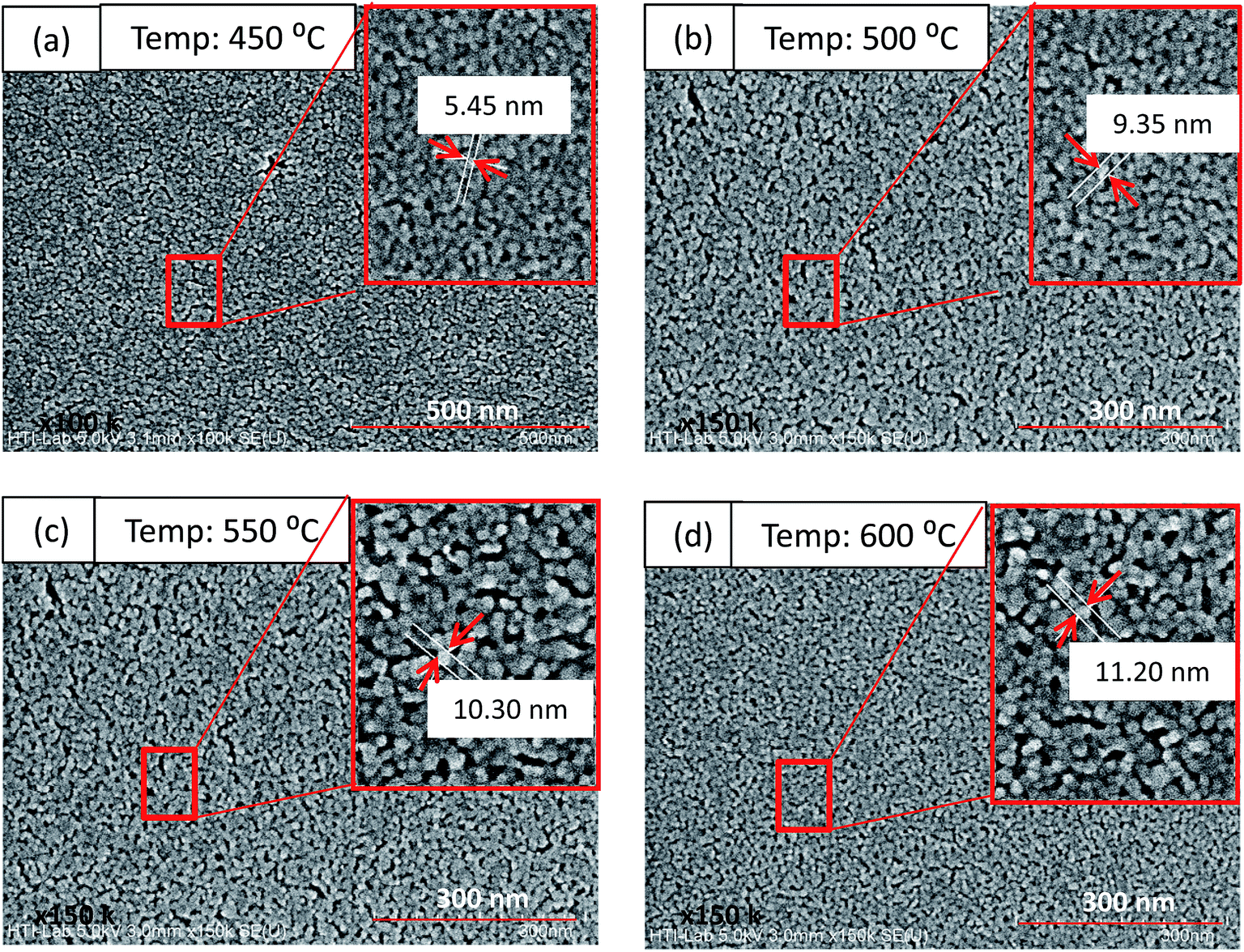 | ||
| Fig. 3 FESEM top view images of the Co catalyst nanoparticles from various post-heat treatment temperatures: (a) 450, (b) 500, (c) 550, and (d) 600 °C. Note that, for clarity, only (a) has a different scale. | ||
Diameter analysis of the as-prepared Co nanoparticles is also shown in Fig. 4, supported by the HRTEM observations. The particle size distribution trend for the post-heat treatment temperature of 450 °C for the 30 measured particles, n = 30, was more similar to a normal distribution compared with the other post-heat treatment temperatures. The normal distribution for that particular histogram shows that the average size of the particles for that sample was 10.64 nm (Fig. 4(a)). The particle size distribution for the post-heat treatment temperatures within the range of 500–600 °C show a fluctuating trend (Fig. 4(b)–(d)). Based on this trend, the distribution of the tube diameter of the CNTs grown on those nanoparticles is considered to be fluctuating as well. Therefore, the post-heat treatment temperature of 450 °C is the optimum temperature for Co catalyst nanoparticle formation, which would lead to a good distribution of the CNT tube size.
 | ||
| Fig. 4 Diameter analysis of the Co catalyst nanoparticles when post-heated at (a) 450, (b) 500, (c) 550, and (d) 600 °C; (e) average particle size of the Co catalyst nanoparticles at the four different post-heat treatments; (f) HRTEM image of the Co nanoparticles on a SiO2 base (sample preparation using FIB). | ||
Based on the enlarged images at the right top corner of every image, the size of the Co catalyst nanoparticles is slightly increased by increasing the post-heat treatment temperature. The changes in the Co catalyst nanoparticle size are affected by the increment of the post-heat temperature. Hence, the post-heat temperature is a critical factor that should be controlled to obtain the desired size of catalyst nanoparticles. The average size of the Co catalyst nanoparticles increases with increasing post-heat temperature. The smallest average diameter of the Co catalyst nanoparticles with a diameter of 10.64 nm was found for the post-heat treatment of 450 °C (Fig. 4(e)). This value was confirmed using HRTEM results with a diameter of approximately 10.67 nm. Meanwhile, the largest average size of the Co catalyst nanoparticles was at the post-heat temperature of 600 °C. Additionally, the Co catalyst nanoparticles formed at different post-heat treatment temperatures were round in shape (Fig. 4(f)).
In principle, a particle needs a specific energy to turn from a gel state into a particle state. If excess energy is present in the system, that energy would then turn the small particle into a large particle. When the size of the particle reaches its limit, the grain of that particular particle would open up and form a necking; subsequently, the particle combines with the particle next to it. If this phenomenon occurs, a crystalline structure could be obtained.25 Therefore, to prevent this phenomenon, determining an optimum temperature for Co catalyst nanoparticle formation is crucial. In the present study, 450 °C is the optimum post-heat treatment temperature for Co catalyst nanoparticle formation.
Surface properties of the Co catalyst films and nanoparticles
 | ||
| Fig. 5 XPS spectra of the pre-heated Co catalyst films for (a) a survey spectrum and (b) a narrow spectrum of Co 2p of the Co oxide system. Note that asterisks * represent the shake-up satellite peaks of Co 2p. | ||
The Co 2p3/2 XPS spectrum of the CoO compound consists of a broad main peak and a very intense shake-up satellite.26 A shake-up satellite is a peak that exhibits a shoulder at both primary spin–orbit sides.27 This peak is used as a fingerprint for the recognition of high-spin Co(II) species in CoO.27,28 The shake-up satellite found for the Co 2p3/2 spin–orbital is intense because it can be clearly seen in the narrow spectrum; this satellite is located at about 4.4 eV above the primary Co 2p3/2 peak. Thus, it is suggested that the CoO compound is present in the pre-heated samples, and the XPS spectrum behavior indicates that the post heated catalyst Co nanoparticles are Co metal covered by a CoO shell.29
The Co 2p region was also observed in the survey spectrum of the Co catalyst nanoparticles (Fig. 6(a)). The primary spin–orbital BE came from 794.8 (Co 2p1/2) and 778.8 eV (Co 2p3/2) (Fig. 6(b)). Both signals were separated by 16 eV. This difference value is consistent with previous studies.27,30 The shake-up satellite observed for the Co 2p3/2 spin–orbital is less intense as it almost disappears in the narrow spectrum; this satellite is located at about 3.7 eV above the primary Co 2p3/2 peak.
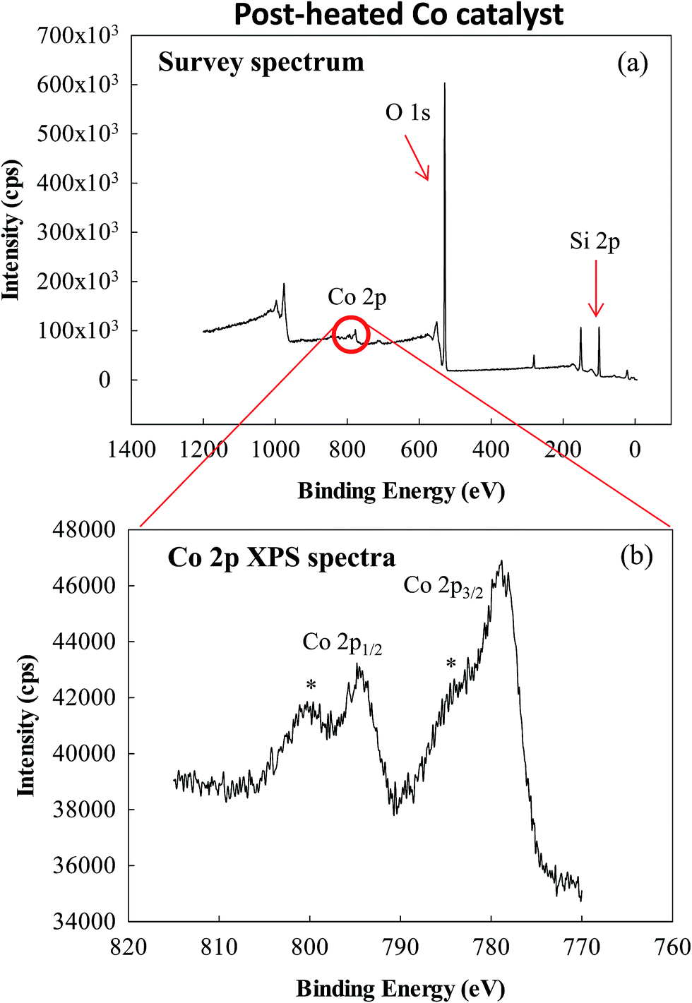 | ||
| Fig. 6 XPS spectra of the post-heated Co catalyst nanoparticles for (a) a survey spectrum and (b) a narrow spectrum of Co 2p of the Co oxide system. Note that asterisks * represent the shake-up satellite peaks of Co 2p. | ||
By comparing the Co 2p narrow spectra of Co catalyst thin film (pre-heated Co) and Co catalyst nanoparticles (post-heated Co), the Co 2p3/2 shake-up satellite of the pre-heated Co was observed to be more intense compared with the post-heated Co (Fig. 7). The difference in the intensity of both shake-up satellites confirmed that Co3O4 is present in the post-heated Co. This result is supported by a report mentioning that Co 2p3/2 of the Co3O4 compound consists of a much smaller shake-up satellite compared with that of the CoO compound.26 Hence, these findings support the previous findings that the CoO and Co3O4 compounds are present on both the pre-heated Co catalyst thin film and the post-heated Co catalyst nanoparticles, respectively.
 | ||
| Fig. 7 Comparison of the Co 2p narrow spectra for pre-heated and post-heated Co samples. Note that asterisks * represent the shake-up satellite peaks of Co 2p. | ||
 | ||
| Fig. 8 XRD patterns of the Co samples prepared on SiO2/Si substrates at various post-heated and constant pre-heated temperatures. | ||
CNT growth through alcohol catalytic CVD
 | ||
| Fig. 9 (a) Raman results within the broad Raman shift range of 50–1800 cm−1; (b) RBM area of the grown CNTs (within the range of 100–400 cm−1); and (c) D- and G-bands of the Raman peaks for the CNTs grown at various CVD processing temperatures. | ||
RBM peaks could be found within the Raman shift range of 100–400 cm−1.4,36 This is a finger print for the presence of SWCNTs and DWCNTs in the Raman spectrum.37 The presence of an RBM region in the Raman spectrum shows that SWCNTs are present on the samples.38 In the plotted Raman spectra, RBM peaks were detected within the Raman shift range of 169–335 cm−1 (Fig. 9(a)). To initiate the growth of SWCNTs or DWCNTs, the catalyst particles should be sufficiently small, with a diameter or DWCNT inner diameter of 1–2 nm.39 Although in total the Co catalyst nanoparticles were found to have average diameter of 10.64 nm, smaller Co nanoparticles were also presence as evidenced from Raman analysis. Confirmation of the CNT structures will be discussed in a later part of this manuscript.
The intensity of the D-band was much lower than that of the G-band (Fig. 9(c)); the height of the former was about a quarter of the latter. By increasing the CVD processing temperature from 650 °C to 700 °C, the G-band intensities were increased accordingly. Meanwhile, when the CVD processing temperature was increased up to 750 °C, the G-band intensities were decreased; the same trend applies to the D-band intensities. The D-band indicates the amorphous content in the samples, whereas the G-band corresponds to the tangential modes of the graphitic planes in CNTs.4,40 Thus, the carbon was highly graphitized at the CVD processing temperature of 700 °C.
Another peak at the left shoulder of the G-band at a Raman shift of around 1550 cm−1 was observed (Fig. 9(c)). The presence of this peak, which was labeled as a G1-band, was found in the Raman spectrum for all CVD processing temperatures. This characteristic, similar to RBM, was specific to SWCNTs. Normally, the G1-band could be observed when the particular samples were inspected using the excitation energy in the green or blue range of visible light. This peak could also be detected when the typical tube diameters were around 1.4 nm.41 Therefore, along with the presence of the RBM region, this G1-band could be used to confirm that SWCNTs are grown on the spin-coated Co catalyst nanoparticles.
The IG/ID ratio is used as an indicator to determine the quality of the as-grown CNTs. By increasing the CVD processing temperature from 650 °C to 700 °C, the IG/ID ratio was also increased (Fig. 10). However, the ratio values decreased when the CVD processing temperature was increased up to 750 °C. A higher IG/ID ratio value indicates that the as-grown CNTs are good quality and have a low amount of defects. The highest IG/ID ratio calculated shows that the optimum temperature to grow good quality CNTs using the ACCVD technique is at a CVD processing temperature of 700 °C.
| IG/ID ratio = G-band intensity/D-band intensity | (1) |
 | ||
| Fig. 10 The IG/ID ratios of the as-grown CNTs at different CVD temperatures. | ||
The RBM region was found within the range of 100–400 cm−1 (Fig. 9(b)). In the RBM region, nine obvious peaks were observed; the 8th peak is the Si peak. Moreover, two dominant peaks, namely the 5th and 6th peaks, were also present in the RBM region. These two peaks were the strongest peaks at the CVD processing temperature of 700 °C compared with the other CVD processing temperatures. These two dominant peaks consistently appeared at all CVD processing temperatures, thus the dominant peaks were confirmed to belong to the CNTs grown on the spin-coated Co catalyst nanoparticles with the spin speed of 8000 rpm and post-heat treatment temperature of 450 °C using the ACCVD technique. The CVD processing temperature of 700 °C was confirmed as the optimum CVD processing temperature to grow good quality SWCNTs. These findings are significant to the statement that Co is a superior catalyst for SWCNT growth (Table 1).42–44
| TCVD (°C) | IG/ID ratio | ID/IG ratio |
|---|---|---|
| 650 | 3.94 | 0.25 |
| 675 | 4.52 | 0.22 |
| 700 | 6.40 | 0.16 |
| 725 | 4.09 | 0.24 |
| 750 | 3.88 | 0.26 |
Furthermore, the SWCNT diameter was not affected by the increase of the CVD processing temperature (Fig. 11). The tube diameter of the as-grown SWCNTs is dependent on the catalyst nanoparticle size.4,45 Moreover, SWCNT growth could be initiated by catalyst particles as small as 1–2 nm in diameter. The as-grown CNT tube diameter may be the same size or smaller than the size of the catalyst nanoparticles. The calculated SWCNT tube diameters were within the range of 0.75–1.48 nm, which was less than 2 nm; therefore, the Co catalyst nanoparticle size during the growth process coincides with that range.
| SWCNT diameter, dtube = 248/RBM | (2) |
 | ||
| Fig. 11 Statistical analysis of the average SWCNT diameter at different CVD processing temperatures. Inset is the table for the analysis. | ||
SWCNTs with smaller tube diameters have good potential for applications in electronic devices.46–48 The SWCNT tube diameters measured in this study were around 1.4 nm or less. Moreover, at the left shoulder of the dominant G-band is another peak called the G1-band. This peak could be analyzed when the typical tube diameter is around 1.4 nm.41
 | ||
| Fig. 12 HRTEM observations of (a) mixture/agglomerated CNTs, (b) the spaghetti-like CNT structure and its length, (c) a DWCNT structure and (d) confirmation of a tip-growth mode for CNTs. | ||
Conclusions
In conclusion, Co catalyst particles with diameters of less than 20 nm could be achieved using a spin coating process. The thickness of the catalyst thin films could be controlled by controlling the spin coating speed. When the spin speed was increased, the thickness decreased because of shear thinning. Meanwhile, the catalyst particle size could be controlled by controlling the heat treatment temperature. For particle formation, when the heat treatment temperature was increased, the particle size became larger because of cluster formation. Therefore, the particle size and film thickness could be controlled by determining the suitable parameters for the spin speed and heat treatment temperature.Acknowledgements
The authors are grateful to the financial support by the Ministry of Higher Education of Malaysia, under the Exploratory Research Grant Scheme with research grant number ERGS/1/2013/TK04/UTEM/02/01/E00032.References
- M. A. Azam, N. S. A. Manaf, E. Talib and M. S. A. Bistamam, Ionics, 2013, 19, 1455 CrossRef CAS.
- N. S. A. Manaf, M. S. A. Bistamam and M. A. Azam, ECS J. Solid State Sci. Technol., 2013, 2, M3101 CrossRef.
- M. A. Azam, M. W. Abd Rashid, K. Isomura, A. Fujiwara and T. Shimoda, Adv. Mater. Res., 2012, 620, 213 CrossRef.
- C.-M. Seah, S.-P. Chai, S. Ichikawa and A. R. Mohamed, Carbon, 2012, 50, 960 CrossRef CAS.
- M. Kumar and Y. Ando, J. Nanosci. Nanotechnol., 2010, 10, 3739 CrossRef CAS PubMed.
- M. Abu-Abdeen and A. A. Aljaafari, Mater. Sci. Appl., 2011, 2, 922 CAS.
- Y. Murakami, Y. Miyauchi, S. Chiashi and S. Maruyama, Chem. Phys. Lett., 2003, 377, 49 CrossRef CAS.
- B. Bräuer, D. R. T. Zahn, T. Rüffer and G. Salvan, Chem. Phys. Lett., 2006, 432, 226 CrossRef.
- B. W. Shivaraj, H. N. Narasimha Murthy, M. Krishna and S. C. Sharma, International Journal of Thin Films Science and Technology, 2013, 2, 143 CrossRef.
- Y. Murakami, Y. Chiashi, Y. Miyauchi, M. Hu, M. Ogura, T. Okubo and S. Maruyama, Chem. Phys. Lett., 2004, 385, 298 CrossRef CAS.
- H. Sugime, S. Noda, S. Maruyama and Y. Yamaguchi, Carbon, 2009, 47, 234 CrossRef CAS.
- M. A. Azam, K. Isomura, A. Fujiwara and T. Shimoda, Phys. Status Solidi A, 2012, 209, 2260 CrossRef CAS.
- N. Inami, M. A. Mohamed, E. Shikoh and A. Fujiwara, Sci. Technol. Adv. Mater., 2007, 8, 292 CrossRef CAS.
- T. Izak, T. Danis, M. Vesely, M. Marton and M. Michalka, Vacuum, 2008, 82, 134 CrossRef.
- P. Baraldi, Spectrochim. Acta, Part A, 1983, 38, 51 CrossRef.
- M. Abu-Abdeen, Mater. Sci. Appl., 2011, 2, 922 CAS.
- M. A. Azam, M. A. Mohamed, E. Shikoh and A. Fujiwara, Jpn. J. Appl. Phys., 2010, 49, 02BA04 CrossRef.
- G. A. Luurtsema, Dissertation, University Of California, Berkeley, 1997.
- B. W. Shivaraj, H. N. N. Murthy, M. Krishna and S. C. Sharma, International Journal of Thin Films Science and Technology, 2013, 2, 143 CrossRef.
- W. Gong, H. Li, Z. Zhao and J. Chen, J. Appl. Phys., 1991, 69, 5119 CrossRef CAS.
- D. B. Hall, P. Underhill and J. M. Torkelson, Polym. Eng. Sci., 1998, 38, 2039 CAS.
- D. E. Bornside, C. W. Macosko and L. E. Scriven, J. Imaging Technol., 1987, 13, 122 CAS.
- S. A. Kamaruddin, K.-Y. Chan, H.-K. Yow, M. Z. Sahdan, H. Saim and D. Knipp, Appl. Phys. A: Mater. Sci. Process., 2011, 104, 263 CrossRef CAS.
- J. Li, J. Xu, Q. Xu and G. Fang, J. Alloys Compd., 2012, 542, 151 CrossRef CAS.
- K.-S. Kim, W.-R. Myung and S.-B. Jung, Electron. Mater. Lett., 2012, 8, 309 CrossRef CAS.
- V. M. Jiménez, A. Fernáindez, J. P. Espinós and A. R. Gonzádez-Elipe, J. Electron Spectrosc. Relat. Phenom., 1995, 71, 61 CrossRef.
- D. Barreca and C. Massignan, Chem. Mater., 2001, 13, 588 CrossRef CAS.
- J. Haber and L. Ungier, J. Electron Spectrosc. Relat. Phenom., 1997, 12, 305 CrossRef.
- H. T. Yang, C. M. Shen, Y. G. Wang, Y. K. Su, T. Z. Yang and H. J. Gao, Nanotechnology, 2004, 15, 70 CrossRef CAS.
- M. A. Azam, A. Fujiwara and T. Shimoda, Appl. Surf. Sci., 2011, 258, 873 CrossRef CAS.
- H. Schulz, W. Denner and H. d’Amour, Acta Crystallogr., Sect. B: Struct. Crystallogr. Cryst. Chem., 1979, 35, 550 CrossRef.
- N. Koshizaki, A. Narazaki and T. Sasaki, Scr. Mater., 2001, 44, 1925 CrossRef CAS.
- S. G. Kandalkar, J. L. Gunjakar and C. D. Lokhande, Appl. Surf. Sci., 2008, 254, 5540 CrossRef CAS.
- A. Mahmoodi, M. Ghoranneviss, M. Mojtahedzadeh, S. H. H. Hosseini and M. Eshghabadi, Int. J. Phys. Sci., 2012, 7, 949 CAS.
- H. R. Barzegar, F. Nitze, T. Sharifi, M. Ramstedt, C. W. Tai, A. Malolepszy, L. Stobinski and T. Wågberg, J. Phys. Chem. C, 2012, 116, 12232 CAS.
- C. Portet, P. L. Taberna, P. Simon and E. Flahaut, J. Power Sources, 2005, 139, 371 CrossRef CAS.
- H. Kim, J. Kang, Y. Kim, B. H. Hong, J. Choi and S. Iijima, J. Nanosci. Nanotechnol., 2011, 11, 470 CrossRef CAS PubMed.
- S. Noda, K. Hasegawa, H. Sugime, K. Kakehi, Z. Zhang, S. Maruyama and Y. Yamaguchi, Jpn. J. Appl. Phys., 2007, 46, L399 CrossRef CAS.
- L. I. Wei, B. O. Wang, D. Liu and L. Li, World Scientific, 2009, 4, 99 CAS.
- H. Kim, J. Kang, Y. Kim, B. H. Hong, J. Choi and S. Iijima, J. Nanosci. Nanotechnol., 2011, 11, 470 CrossRef CAS PubMed.
- N. Grobert, Kleine Röhren: Carbon Nanotubes: Basic Concepts and Physical Properties, ed. V. S. Reich, C. Thomson and J. Maultzsch, Wiley-VCH, Weinheim, 2004, ISBN 3-527-40386-8, DOI:10.1002/nadc.20040520924.
- S. M. Bachilo, L. Balzano, J. E. Herrera, F. Pompeo, D. E. Resasco and R. B. Weisman, J. Am. Chem. Soc., 2003, 37, 11186 CrossRef PubMed.
- Y. Chen, D. Ciuparu, S. Y. Lim, Y. H. Yang, G. L. Haller and L. Pfefferle, J. Catal., 2004, 2, 453 CrossRef.
- Y. Chen, D. Ciuparu, S. Lim, Y. H. Yang, G. L. Haller and L. Pfefferle, J. Catal., 2004, 2, 351 CrossRef.
- H. Dai, A. G. Rinzler, P. Nikolaev, A. Thess, D. T. Colbert and R. E. Smalley, Chem. Phys. Lett., 1996, 260, 471 CrossRef CAS.
- K. H. An, K. K. Jeon, J. K. Heo, S. C. Lim, D. J. Bae and Y. H. Lee, J. Electrochem. Soc., 2002, 149, A1058 CrossRef CAS.
- K. H. An, W. S. Kim, Y. S. Park, Y. C. Choi, S. M. Lee, D. C. Chung, D. J. Bae, S. C. Lim and Y. H. Lee, Adv. Mater., 2001, 13, 497 CrossRef CAS.
- K. H. An, W. S. Kim, Y. S. Park, J.-M. Moon, D. J. Bae, S. C. Lim, Y. S. Lee and Y. H. Lee, Adv. Funct. Mater., 2001, 11, 387 CrossRef CAS.
- M. S. A. Bistamam and M. A. Azam, Results Phys., 2014, 4, 105 CrossRef.
| This journal is © The Royal Society of Chemistry 2015 |