Towards near-infrared photosensitization of tungsten trioxide nanostructured films by upconverting nanoparticles

Frédéric Venne a, Marta Quintanilla b, Francis Quenneville a, Dilek Işik a, Bill Baloukas a, Fiorenzo Vetrone bc and Clara Santato *ad
aDepartment of Engineering Physics, Polytechnique Montréal, C.P. 6079 Succ. Centre Ville, Québec H3C 3A7, Canada. E-mail: clara.santato@polymtl.ca
bInstitut National de la Recherche Scientifique – Énergie, Matériaux et Télécommunications (INRS – EMT), Université du Québec, 1650 Boul. Lionel-Boulet, Varennes, QC J3X 1S2, Canada
cCentre for Self-Assembled Chemical Structures, McGill University, Montreal, Canada
dRegroupement Québécois sur les Matériaux de Pointe (RQMP), Canada

Received 8th September 2015 , Accepted 16th September 2015

First published on 18th September 2015


Abstract

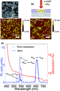
Upconverting materials are currently explored in the field of solar energy conversion in order to extend the light harvesting properties of semiconductors to the near-infrared (NIR) region, their absorption being generally limited to the visible region of the solar spectrum. Here, we propose to photosensitize nanostructured films of tungsten oxide (WO3), a semiconductor widely investigated in photoelectrochemistry, photocatalysis and electrochromics, with NaGdF4:Er3+, Yb3+ upconverting nanoparticles (UCNPs). In order to do so, we fabricate nanocomposite films of WO3 and NaGdF4:Er3+, Yb3+ UCNPs (indicated as UCNP/WO3 films). Current–time measurements show that, under irradiation at λ = 980 nm, a relative increase in current of about 3% with respect to the dark current is observed in the UCNP/WO3 films. The UCNP/WO3 mol% ratio and the temperature of the thermal treatment of the nanocomposite films are both critical to simultaneously achieve photosensitization and charge carrier transport in the UCNP/WO3 films.


Introduction

Photovoltaic (PV) solar energy conversion contributes to the fulfilment of the increasing world energy demands.1 Different approaches have been investigated to overcome the Shockley–Queisser limit, which is the theoretical maximum efficiency attainable by a single-junction PV cell. For example, multi-junction cells are intended to match the solar spectrum by stacking materials with increasing bandgaps.2 Approaches based on optical processes, such as two-photon absorption (simultaneous absorption of two photons by a material), downconversion (conversion of a high-energy photon to several lower-energy photons) or upconversion (conversion of several low-energy photons into one higher-energy photon) are also intensively pursued.3–5

High surface area, mesoporous, transparent nanostructured films of metal oxides, such as TiO2 and WO3, have been widely investigated for solar energy conversion (photocatalysis and photoelectrochemistry) and energy conservation (electrochromism).6–9 However, their large bandgaps (ca. 3.1 eV for TiO2 and 2.5 eV for WO3) render imperative the search for strategies to improve their solar light absorption properties, from the viewpoint of practical PV applications. In particular, the photoresponse of WO3 extends to 500 nm, such that photons of lower energy, e.g. NIR photons, are not harvested to generate photocurrent, thus leading to considerable energy losses.10,11 The use of upconverting (UC) materials represents a possible strategy to mitigate these losses since these materials absorb NIR photons and convert them to a frequency range that can then be absorbed by the metal oxide.

UC materials have been incorporated into different PV cell structures, including crystalline silicon,12 amorphous silicon,13 dye-sensitized,14,15 and organic16 solar cells. In addition, UC materials with different chemical compositions have been investigated, such as rare earth and transition metal ions,17–20 semiconductor quantum dots,21–23 and metallated macrocycles.24–28 In UC materials, the excitation of the higher energy emitting states occurs via the sequential absorption of multiple NIR photons. In particular, in lanthanide-based UC materials, upconversion occurs via the sequential absorption of multiple NIR photons through real long-lived 4f excited electronic states. This is in stark contrast to conventional two-photon absorption (TPA) materials where two photons are absorbed simultaneously (or within less than a nanosecond), populating an excited state that is the sum of the energy of the incident photons.20 Because of the extremely short lifetime of the (virtual) intermediate states, TPA can only be efficient with high-intensity photon fluxes (e.g., ultrafast laser radiation). On the other hand, the relatively long lifetime (μs to ms) of the 4f excited states of Ln3+ ions, such as Pr3+, Nd3+, Sm3+, Dy3+, Ho3+, Er3+, and Tm3+,29 make them easily excited with low-power continuous wave NIR diodes30,31 and suitable for up-converting lower intensity solar radiation. Fluoride-based crystals, in particular NaGdF4, are commonly employed as host materials for lanthanide dopants, due to their low phonon energies, helping to limit non-radiative relaxation processes.32

UC materials are often included in a solar energy conversion system in the form of an external layer, with different possible configurations, such as PV cell and rear converter or front converter and PV cell.33,34 On the other hand, the use of UC nanoparticles (UCNPs) in intimate contact with nanostructured semiconductors has the potential to maximize the synergy between the two nanomaterials.

In this work, we report on the design, fabrication and characterization of nanocomposite films based on sol–gel prepared WO3 and NaGdF4:Er3+, Yb3+ UCNPs to improve the absorption properties of WO3 nanostructured films in the NIR region of the solar spectrum. For the first time, UCNPs and pure metal oxides are used to produce nanocomposite films in which a photocurrent can be generated upon NIR irradiation. Er3+ is ideally suited for up-conversion since its electronic structure allows for many radiative transitions to occur (see Fig. S1). Er3+ is often co-doped with Yb3+. Co-doping with the Yb3+ ion has been shown to improve the intensity of the up-conversion emission compared to singly doped systems since Yb3+ possesses only one excited state with a very high absorption cross-section in the NIR (ca. 980 nm), which leads to efficient energy transfer to the 4I11/2 state of Er3+ also located at approximately 980 nm. Our solution to use NaGdF4:Er3+, Yb3+ UCNPs to photosensitize WO3 is based on the fact that, when excited at λexc = 980 nm, the UCNPs have two emission bands in the visible range, partly overlapping with the absorption spectrum of WO3,20,35 thus leading to the possibility to use them as photosensitizers. The measure of the photocurrent generated by UCNP/WO3 nanocomposite films in a planar configuration under NIR irradiation (λexc = 980 nm) confirmed the interest of our strategy. Atomic Force Microscopy (AFM), X-ray diffraction (XRD) and photoluminescence (PL) studies were conducted to identify the fabrication conditions to simultaneously achieve good photosensitization and charge carrier transport properties in the UCNP/WO3 films. Our strategy paves the way towards the NIR photosensitization of metal oxide semiconductors for PV applications by simple solution-based processing.

Experimental section

1. Microfabrication of the electrodes

ITO electrodes were patterned by photolithography. The ITO-coated glass substrates (Colorado Concept Coatings, 30 mm × 30 mm, <15 Ω square−1 sheet resistance) were first sequentially cleaned in an ultrasonic bath in isopropyl alcohol (IPA), acetone, and IPA for 15 min each, and N2-dried. Then, prior to the microfabrication steps, the substrates were exposed to a UV-ozone treatment for 15 min. After selective exposure and development of a positive-tone photoresist layer, the ITO film was chemically etched with hydrochloric acid (HCl[thin space (1/6-em)]:[thin space (1/6-em)]H2O 65 v/v%) and the unexposed photoresist was removed with acetone. This process resulted in ITO electrodes with an interelectrode spacing, L, of 100 μm and a width, W, of 6000 μm.

2. Materials and film fabrication

The WO3 films were prepared following a sol–gel synthesis process already reported in the literature.10 Na2WO4, PEG-200, ethanol and the proton-exchange resin (Dowex® 50WX2) were purchased from Sigma Aldrich. NaGdF4:Er3+, Yb3+ (2 mol% Er3+, 20 mol% Yb3+) UCNPs were prepared via a thermal decomposition process also reported in the literature.35 First, lanthanide trifluoroacetates used as precursors in the synthesis were prepared from lanthanide oxides (Alpha Aesar, Gd2O3, Er2O3, Yb2O3, >99.99%) in deionized water and trifluoroacetic acid (Alpha Aesar, 99%).36 In the standard process, the obtained precursors, together with the required stoichiometric quantities of sodium trifluoroacetate (Sigma-Aldrich, 98%), were injected at a rate of 1.0 mL min−1 in a 1[thin space (1/6-em)]:[thin space (1/6-em)]1 solution of oleic acid (Alpha Aesar, 90%) and octadecene (Alpha Aesar, 90%) at 315 °C, and aged for 1 h. The prepared β-phase NaGdF4:Er3+, Yb3+ UCNPs were then washed by centrifugation and redispersed in hexane. The LiYF4:Tm3+, Yb3+ UCNPs were synthesized using a similar technique with slight modifications (mainly, the precursors weren't injected. Instead, they were mixed with oleic acid and octadecene from the very beginning).37 In this case, the oxides Y2O3, Tm2O3 were used to prepare the trifluoroacetates precursors and lithium trifluoroacetate was used in the reaction that was done at 325 °C. The synthesized UCNPs were capped with long-chained oleate molecules making them hydrophobic. To render them hydrophilic and to avoid any possible effect of the capping agent in the final material, the oleates were removed by following a process described in literature.38 NaGdF4:Er3+, Yb3+ UCNPs had a narrow size distribution, with a diameter of 45 nm (see Fig. 1a), and showed a hexagonal-nanoplate shape typical of the β-phase of NaGdF4.
image file: c5ra18320k-f1.tif
Fig. 1 (a) TEM image of β-NaGdF4:Er3+, Yb3+ UCNPs. (b) Experimental configuration adopted in this work for the electrical characterization (photocurrent vs. time). Topographical AFM images of (c) WO3 and (d) 8 mol% UCNP/WO3 films, deposited on glass and treated at 385 °C. (e) PL spectrum of β-NaGdF4:Er3+, Yb3+ UCNPs drop casted on glass and dried at room temperature (dashed line, left y axis) or thermally treated at 385 °C (full line, left y axis) and optical absorption spectrum of a WO3 film (∼1.2 μm in thickness), deposited on glass and thermally treated at 385 °C (right y axis).

To fabricate the nanocomposite films, a mixture containing 1% weight/weight concentration of UCNPs suspension in water and ca. 0.3 M tungstic acid sol was prepared to reach different mol% UCNP/WO3 (6, 8, and 16 mol%). The mixture was aged for about 1 h under continuous stirring before film deposition. Nanocomposite films were obtained by drop-casting 10 μL UCNP/WO3 mixture (or pure WO3 sol for control films) on ITO-patterned substrates, followed by a thermal treatment at 385 °C, in O2 (160 scc min−1), for 30 min.

3. Characterization techniques

Photoluminescence measurements were carried out with a Prism And Reflector Imaging Spectroscopy System (PARISS, purchased from LightForm Inc.) in ambient air conditions after excitation at λexc = 980 nm from a cw NIR laser diode (power density of 1 W cm−2). The specular and diffuse transmission/reflection properties of the WO3 films were assessed using a PerkinElmer Lambda 1050 UV/Vis/NIR spectrophotometer equipped with a Labsphere integration sphere. The use of an integration sphere allows one to take into account light diffusion which could potentially be wrongly associated with losses due to absorption in purely specular-type measurements. The absorption (A) was calculated using the following equation: A = 100% − TRD where T, R and D are the specular transmission, specular reflection and total diffusion respectively. The microstructure of the samples was characterized by XRD (Bruker D-8 Advance Diffractometer), using CuKα radiation. High-resolution transmission electron microscopy (TEM, Philips CM200) was used to ascertain the phase, morphology, crystallinity and size distribution of the UCNPs. Atomic force microscopy (AFM) images were obtained in ambient air conditions using a Veeco Dimension 3100 Digital Instruments with a Si cantilever (tip radius < 10 nm, spring constant 40 N m−1) at a scan rate of 1 Hz. Photocurrent–time measurements were carried out in a planar configuration (see Fig. 1b), in ambient air conditions, using a B2902A Agilent Source Measure Unit (SMU). Measurements under simulated solar irradiation (AM1.5G) were performed using a VeraSol-2 LED solar simulator (Newport).

Results and discussion

1. Film fabrication and characterization

To achieve the successful combination of UCNPs and nanostructured WO3 in a nanocomposite film, a number of challenges had to be overcome.

First, since UCNPs are electrically insulating, it was imperative to identify the optimal UCNP/WO3 mol% ratio to photosensitize WO3 without hindering charge transport in the nanocomposite films. In order to do so, we prepared films with different UCNP/WO3 mol% ratios. Films prepared at ratios above 8 mol% were discontinuous, i.e. not easily amenable for incorporation into devices (see Fig. S2). No significant effect of the presence of UCNPs on the photocurrent was observed in films with ratios below 8 mol% (see Fig. S3). The morphology of 8 mol% UCNP/WO3 films (Fig. 1d) was similar to that of WO3 control films (Fig. 1c). 8 mol% UCNP/WO3 films, similarly to the case of WO3 control films, showed complete substrate surface coverage. Furthermore, 8 mol% UCNP/WO3 films showed no evidence of phase segregation and values of surface roughness (RRMS) comparable to those of WO3 films (0.8 nm vs. 0.9 nm). Therefore, overall, 8 mol% UCNP/WO3 films showed to be of device quality.

Secondly, we had to identify the optimal temperature for the thermal treatment of the nanocomposite films to ensure good charge transport, while keeping a high UCNPs emission, essential for photosensitization. Achieving good transport properties in nanostructured WO3 films synthesized by sol–gel methods usually requires thermal treatment temperatures within the range of 350–600 °C.39,40 However, such high temperatures would affect the crystalline structure of UCNPs. Indeed, a change from the hexagonal phase (β-UCNPs) to the cubic phase (α-UCNPs) is expected to take place at temperatures as low as 400 °C.41 Most importantly, the upconverting process is reported to be one order of magnitude more efficient in β-phase NaGdF4:Er3+, Yb3+ UCNPs than in α-UCNPs, for the nanoparticle size used here.42 To avoid, at least in part, this phase transformation, we treated the UCNP/WO3 films at 385 °C. The comparison of the PL spectrum of 45 nm-sized NaGdF4:Er3+, Yb3+ β-UCNPs treated at 385 °C with the optical absorption spectrum of ∼1.2 μm-thick WO3 films treated at 385 °C shows the partial overlap of the WO3 absorption and the UCNPs emission spectra (see Fig. 1e). Such an overlap represents an interesting opportunity to photosensitize WO3 films in the NIR region and constitutes the foundation of our strategy. In addition, two emission bands located at ca. 550 nm and ca. 660 nm are observable upon NIR laser excitation (λexc = 980 nm, power density of 1 W cm−2) in the PL spectra of the UCNPs, both after room temperature drying and 385 °C thermal treatment (Fig. 1e). The green emission band located at ca. 550 nm is attributed to transitions from the 2H11/2 and 4S3/2 excited states to the 4I15/2 ground state of Er3+ ions (see Fig. S1). The red emission band observed at ca. 660 nm is attributed to the transition from the 4F9/2 excited state to the 4I15/2 ground state.22Fig. 1e shows that the thermal treatment affects the emission properties of the UCNPs such that the green[thin space (1/6-em)]:[thin space (1/6-em)]red intensity ratio is about 1 when the UCNPs are dried at room temperature, whereas this ratio is ∼0.3 after treatment at 385 °C.

XRD measurements were then performed to gain insight on the dependence of the PL properties on the temperature of thermal treatment (see Fig. 2). When dried at room temperature (RT) on glass, the XRD peaks of NaGdF4:Er3+, Yb3+ UCNPs (pattern 1) match the filed pattern of NaGdF4 with a hexagonal crystal phase (β-phase).43,44 When the UCNPs are thermally treated at 385 °C (pattern 2), UCNPs are likely to remain in the β-phase, as suggested by the presence of the peaks at 30°, 43°, and 52°. The positions of the peaks of the cubic phase (α-UCNPs) are also indicated in Fig. 2, to validate the hypothesis that UCNPs are not in the α-phase after the thermal treatment. The comparison between pattern 1 and 2 show that the relative intensity of the peaks changes from pattern 1 to pattern 2 thus suggesting that the UCNPs reorient during thermal treatment. This reorientation can account for the observed differences in the upconverted red and green emissions since NaGdF4 is not isotropic.45 The presence of O2 during the thermal treatment has no noticeable effect on the structure of the UCNPs.


image file: c5ra18320k-f2.tif
Fig. 2 XRD patterns of β-UCNPs, 45 nm in diameter, drop casted on glass. After room temperature drying and a thermal treatment at 385 °C, the UCNPs are still in the β-phase (hexagonal phase, patterns 1 and 2). For reference purposes, the peak positions for the α and β phases are included at the bottom of the figure.31

2. Electrical measurements

Current–time measurements were performed using a two-electrode, planar configuration to assess the possibility to generate a photocurrent in UCNP/WO3 nanocomposite films (∼1 μm thick) exposed to NIR light (XRD pattern in Fig. S4). UCNP/WO3 nanocomposite films were systematically compared with WO3 control film samples. During the electrical measurements, the films were initially kept in ambient light conditions for 300 s, followed by 300 s in total darkness, under a constant electrical bias (0.5 V, 0.7 V, or 1.0 V), to allow the dark current to stabilize prior to photocurrent measurements. Afterwards, the samples were illuminated by a cw NIR laser (λexc = 980 nm, power density of 1 W cm−2). Typically, during the electrical measurements the films were exposed for 30 s to light, followed by 60 s in the dark. To describe the effect of the illumination on the current measured, we used the “on/off ratio”, Ron/off, calculated as follows:
Ron/off = 100 × (ionioff)/ioff
where ion is the current when the NIR light illuminated the sample (on current) and ioff is the current in the dark (off current). When 8 mol% UCNP/WO3 films were exposed to NIR light, an increase of the current was observed (Fig. 3a and S5). A value of Ron/off ranging between 3.4 to 3.9% was obtained when the NIR light illuminated the nanocomposite films, depending of the applied electrical bias. This increase in the current is attributable to the absorption of the NIR light by the UCNPs followed by the harvesting of the upconverted light by the WO3, in turn followed by the generation of a photocurrent.

image file: c5ra18320k-f3.tif
Fig. 3 Current–time measurements under NIR chopped light (60 s in the dark and 30 s under irradiation, λexc = 980 nm, power density of 1 W cm−2) for films deposited on patterned ITO with an interelectrode distance of 100 μm and thermally treated at 385 °C made of (a) 8 mol% UCNP/WO3 and (b) WO3. Samples were kept under constant electrical bias for 300 s in ambient light conditions, followed by 300 s in the dark, before chopping the light.

To evaluate the possibility that thermal effects due to laser exposure are responsible for the current increase observed with 8 mol% UCNP/WO3 films exposed to NIR light, we exposed WO3 control films to the NIR laser: no noticeable current increase was observed in this case (see Fig. 3b). These results suggest that the increase in the current measured from 8 mol% UCNP/WO3 nanocomposite films under NIR exposure are most probably the result of a photocurrent induced by the presence of UCNPs, that thermal effects likely play a minor role.

To further demonstrate the light harvesting properties of our films under more realistic lighting conditions, the samples were also exposed to simulated solar irradiation (AM1.5G); a photocurrent was also observed (see Fig. S6) thus confirming that the NIR photosensitization process does not prevent the nanocomposite films to generate photocurrent under simulated solar light, as expected.

The hypothesis that thermal effects play a minor role in the photoresponse of thin films of UCNP/WO3 is supported by results observed with blue-emitting UCNPs, such as LiYF4:Tm3+, Yb3+. Here an improved overlap between the absorption spectrum of WO3 and the emission spectrum of UCNPs with respect to the case of NaGdF4:Er3+, Yb3 is paralleled by the higher values of Ron/off observed (ca. 6%) (see Fig. S7).

Conclusions and perspectives

In conclusion, we have demonstrated an interesting strategy for the photosensitization in the NIR of metal oxide WO3 films based on the addition of UCNPs. Specifically we observed an increase in the current measured in NaGdF4:Er3+, Yb3+/WO3 nanocomposite films under NIR irradiation (λexc = 980 nm), with respect to dark conditions. After a judicious choice of the mol% ratio in the nanocomposite film and the thermal treatment temperature, we demonstrated that nanocomposite films could be engineered so as not to hinder the transport properties in the nanocomposite films while also extending their photosensitivity to NIR light. The approach herein presented is promising for solar energy conversion applications, as it permits to prepare, by an easy solution-based technique, high surface area, nanocomposite films photosensitive to visible and NIR light.

In perspective, there remain several challenges which need to be addressed in order to optimize the use of lanthanide UCNPs as metal oxide photosensitizers in PV cells. Indeed, considering that the absorption bandwidth of the lanthanide-based UCNPs is fairly narrow, the combination of several upconverters within the metal oxide matrix has to be explored. Furthermore, increasing the upconversion quantum yield of UCNPs, which is presently relatively low,41,46 would also lead to performance improvements. In fact, recent reports have proposed approaches to develop systems with increased yield.47,48 Implementing the above-mentioned considerations has the potential to generate significant improvement in the power conversion efficiency of metal oxide-based PV cells in the NIR.

Acknowledgements

The authors are grateful to J. Lerner (LightForm Inc) and P. Moraille for fruitful discussions and to Y. Drolet for his technical support. Authors are grateful to Prof. G. Hanan and Dr D. Chartrand for the access to the solar simulator system. This work was financially supported by: NSERC (Discovery grants C.S. and F.V.), FRQNT Team Grant (C.S. and F.V.), MDEIE (F.V.). F. Venne acknowledges the financial support provided by CMC Microsystems (MNT program) and M. Quintanilla acknowledges the financial support of Fundacion Ramon Areces.

Notes and references

  1. T. M. Razykov, C. S. Ferekides, D. Morel, E. Stefanakos and H. S. Ullal, Sol. Energy, 2011, 85, 1580–1608 CrossRef CAS PubMed.
  2. D. J. Friedman, Curr. Opin. Solid State Mater. Sci., 2010, 14, 131–138 CrossRef CAS PubMed.
  3. X. Huang, S. Han, W. Huang and X. Liu, Chem. Soc. Rev., 2013, 42, 173–201 RSC.
  4. R. Naccache, F. Vetrone and J. A. Capobianco, ChemSusChem, 2013, 6, 1308–1311 CrossRef CAS PubMed.
  5. J. C. Goldschmidt and S. Fischer, Adv. Opt. Mater., 2015, 3, 510–535 CrossRef CAS PubMed.
  6. S. K. Deb, Sol. Energy Mater. Sol. Cells, 2008, 92, 245–258 CrossRef CAS PubMed.
  7. S. H. Baeck, K. S. Choi, T. F. Jaramillo, G. D. Stucky and E. W. McFarland, Adv. Mater., 2003, 15, 1269–1273 CrossRef CAS PubMed.
  8. H. Zheng, Y. Tachibana and K. Kalantar-zadeh, Langmuir, 2010, 26, 19148–19152 CrossRef CAS PubMed.
  9. I. Concina and A. Vomiero, Small, 2015, 11, 1744–1774 CrossRef CAS PubMed.
  10. C. Santato, M. Odziemkowski, M. Ulmann and J. Augustynski, J. Am. Chem. Soc., 2001, 123, 10639–10649 CrossRef CAS PubMed.
  11. P. Ramasamy, M. Palanisamy and J. Kim, RSC Adv., 2014, 4, 34873–34895 RSC.
  12. A. Shalav, B. S. Richards, T. Trupke, K. W. Krämer and H. U. Güdel, Appl. Phys. Lett., 2005, 86, 4–7 CrossRef PubMed.
  13. J. de Wild, J. K. Rath, A. Meijerink, W. G. J. H. M. van Sark and R. E. I. Schropp, Sol. Energy Mater. Sol. Cells, 2010, 94, 2395–2398 CrossRef CAS PubMed.
  14. G.-B. Shan and G. P. Demopoulos, Adv. Mater., 2010, 22, 4373–4377 CrossRef CAS PubMed.
  15. C. Yuan, G. Chen, P. N. Prasad, T. Y. Ohulchanskyy, Z. Ning, H. Tian, L. Sun and H. Ågren, J. Mater. Chem., 2012, 22, 16709–16713 RSC.
  16. H.-Q. Wang, M. Batentschuk, A. Osvet, L. Pinna and C. J. Brabec, Adv. Mater., 2011, 23, 2675–2680 CrossRef CAS PubMed.
  17. M. Pollnau, D. R. Gamelin, S. R. Lüthi and H. U. Güdel, Phys. Rev. B: Condens. Matter Mater. Phys., 2000, 61, 3337–3346 CrossRef CAS.
  18. S. Heer, K. Kömpe, H.-U. Güdel and M. Haase, Adv. Mater., 2004, 16, 2102–2105 CrossRef CAS PubMed.
  19. J. C. Boyer, L. A. Cuccia and J. A. Capobianco, Nano Lett., 2007, 7, 847–852 CrossRef CAS PubMed.
  20. F. Auzel, Chem. Rev., 2004, 104, 139–173 CrossRef CAS PubMed.
  21. X. Wang, W. Yu, J. Zhang, J. Aldana, X. Peng and M. Xiao, Phys. Rev. B: Condens. Matter Mater. Phys., 2003, 68, 1–6 Search PubMed.
  22. C. Bonati, A. Cannizzo, D. Tonti, A. Tortschanoff, F. van Mourik and M. Chergui, Phys. Rev. B: Condens. Matter Mater. Phys., 2007, 76, 1–4 CrossRef.
  23. E. Poles, D. C. Selmarten, O. I. Mićić and A. J. Nozik, Appl. Phys. Lett., 1999, 75, 971 CrossRef CAS PubMed.
  24. R. R. Islangulov, J. Lott, C. Weder and F. N. Castellano, J. Am. Chem. Soc., 2007, 129, 12652–12653 CrossRef CAS PubMed.
  25. T. N. Singh-Rachford and F. N. Castellano, Coord. Chem. Rev., 2010, 254, 2560–2573 CrossRef CAS PubMed.
  26. V. Yakutkin, S. Aleshchenkov, S. Chernov, T. Miteva, G. Nelles, A. Cheprakov and S. Baluschev, Chem.–Eur. J., 2008, 14, 9846–9850 CrossRef CAS PubMed.
  27. S. Baluschev, V. Yakutkin, G. Wegner, T. Miteva, G. Nelles, A. Yasuda, S. Chernov, S. Aleshchenkov and A. Cheprakov, Appl. Phys. Lett., 2007, 90, 1–4 CrossRef PubMed.
  28. S. Baluschev, T. Miteva, V. Yakutkin, G. Nelles, A. Yasuda and G. Wegner, Phys. Rev. Lett., 2006, 97, 7–9 CrossRef.
  29. F. Vetrone, J.-C. Boyer and J. A. Capobianco, Encycl. Nanosci. Nanotechnol., 2004, 10, 725–765 CAS.
  30. J. Yang, L. Zhang, L. Wen, S. Dai, L. Hu and Z. Jiang, J. Appl. Phys., 2004, 95, 3020 CrossRef CAS PubMed.
  31. F. Vetrone, J.-C. Boyer, J. A. Capobianco, A. Speghini and M. Bettinelli, J. Phys. Chem. B, 2003, 107, 10747–10752 CrossRef CAS.
  32. J. F. Suyver, J. Grimm, M. K. van Veen, D. Biner, K. W. Krämer and H. U. Güdel, J. Lumin., 2006, 117, 1–12 CrossRef CAS PubMed.
  33. L. Li, Y. Yang, R. Fan, Y. Jiang, L. Wei, Y. Shi, J. Yu, S. Chen, P. Wang, B. Yang and W. Cao, J. Power Sources, 2014, 264, 254–261 CrossRef CAS PubMed.
  34. T. Trupke, M. A. Green and P. Würfel, J. Appl. Phys., 2002, 92, 4117–4122 CrossRef CAS PubMed.
  35. F. Vetrone, R. Naccache, V. Mahalingam, C. G. Morgan and J. A. Capobianco, Adv. Funct. Mater., 2009, 19, 2924–2929 CrossRef CAS PubMed.
  36. C. Rüssel, J. Non-Cryst. Solids, 1993, 152, 161–166 CrossRef.
  37. T. Cheng, R. F. Ortiz, K. Vedantham, F. Vetrone, R. S. Marks, T. W. J. Steele and B. Sheva, Biomacromolecules, 2015, 16, 364–373 CrossRef CAS PubMed.
  38. N. Bogdan, F. Vetrone, G. A. Ozin and J. A. Capobianco, Nano Lett., 2011, 11, 835–840 CrossRef CAS PubMed.
  39. B. Yang, Y. Zhang, E. Drabarek, P. R. F. Barnes and V. Luca, Chem. Mater., 2007, 19, 5664–5672 CrossRef CAS.
  40. H. Zheng, J. Z. Ou, M. S. Strano, R. B. Kaner, A. Mitchell and K. Kalantar-zadeh, Adv. Funct. Mater., 2011, 21, 2175–2196 CrossRef CAS PubMed.
  41. N. C. Dyck, F. C. J. M. van Veggel and G. P. Demopoulos, ACS Appl. Mater. Interfaces, 2013, 5, 11661–11667 CAS.
  42. A. Aebischer, S. Heer, D. Biner, K. Krämer, M. Haase and H. U. Güdel, Chem. Phys. Lett., 2005, 407, 124–128 CrossRef CAS PubMed.
  43. G. D. Brunton, H. Insley, T. N. McVay and R. E. Thoma, Oak Ridge Natl. Lab. Rep. ORNL (U.S.), 1965.
  44. The peak (0 0 2) has been deduced using the Bragg diffraction law. It was not indexed from 43.
  45. P. Chen, M. Song, E. Wu, B. Wu, J. Zhou, H. Zeng, X. Liu and J. Qiu, Nanoscale, 2015, 7, 6462–6466 RSC.
  46. J.-C. Boyer and F. C. J. M. van Veggel, Nanoscale, 2010, 2, 1417–1419 RSC.
  47. W. Zou, C. Visser, J. A. Maduro, M. S. Pshenichnikov and J. C. Hummelen, Nat. Photonics, 2012, 6, 2–6 CrossRef PubMed.
  48. M. D. Wisser, M. Chea, Y. Lin, D. M. Wu, W. L. Mao, A. Salleo and J. A. Dionne, Nano Lett., 2015, 15, 1891–1897 CrossRef CAS PubMed.

Footnote

Electronic supplementary information (ESI) available: Energy levels diagram of UCNPs; optical images of 16 mol% UCNP/WO3 thin films; current–time curves of 6% UCNP/WO3 thin films; XRD measurements of WO3 and UCNP/WO3 thin films; current–time curves of 8% UCNP/WO3 thin films under NIR and simulated solar light; spectroscopic and current–time measurements on LiYF4:Tm3+, Yb3+/WO3 thin films. See DOI: 10.1039/c5ra18320k

This journal is © The Royal Society of Chemistry 2015
Click here to see how this site uses Cookies. View our privacy policy here.