
Ultrathin amorphous silicon thin-film solar cells by magnetic plasmonic metamaterial absorbers
Chaojun
Tang†
a,
Zhendong
Yan†
b,
Qiugu
Wang†
c,
Jing
Chen
*d,
Mingwei
Zhu
e,
Bo
Liu
f,
Fanxin
Liu
*ab and
Chenghua
Sui
a
aDepartment of Applied Physics, Zhejiang University of Technology, Xiaoheshan, Hangzhou 310023, China. E-mail: liufanxin@zjut.edu.cn
bNational Laboratory of Solid State Microstructures and Department of Physics, Nanjing University, Nanjing 210093, China
cDepartment of Electrical and Computer Engineering, Iowa State University, Ames, Iowa 50011, USA
dCollege of Electronic Science and Engineering, Nanjing University of Posts and Telecommunications, Nanjing 210023, China. E-mail: jchen@njupt.edu.cn
eNational Laboratory of Solid State Microstructures and Department of Materials Science and Engineering, Nanjing University, Nanjing 210093, China
fSchool of Mathematics and Physics, Jiangsu University of Technology, Changzhou 213001, China
First published on 21st September 2015
Abstract
Efficient solar harvesting for ultrathin amorphous silicon (α-Si) films with a thickness of less than 100 nm is critical to the performance of solar cells, since the very short carrier-diffusion length of α-Si and the Staebler–Wronski effect restrict their thickness. In this work, we numerically investigate energy harvesting in metamaterial-based solar cells, in which an ultrathin α-Si film is sandwiched between a silver (Ag) substrate and a square array of Ag nanodisks, and combined with an indium tin oxide (ITO) anti-reflection layer. It is found that only a 20 nm-thick α-Si film is able to absorb over 50% solar energy in the spectral range from 300 to 800 nm at normal incidence, and the amount of absorbed light is equivalent to a photocurrent of about 13.4 mA cm−2. This broadband absorption is achieved by the spectral design on the overlapped absorption peaks which are caused by the excitations of two lowest-order Fabry–Pérot (FP) resonances in the α-Si and ITO layers and a magnetic resonance arising from the plasmon hybridization between Ag disks and the substrate. The absorption performance of our structure is less dependent on the incident angle θ and polarization of light when θ < 20°, but it will decrease dramatically when θ > 70° (20°) for P (S) polarization.
1. Introduction
First-generation crystalline silicon (c-Si) based ‘bulk’ solar cells with a wafer thickness between 180 and 300 μm have average photovoltaic conversion efficiencies in the range of 16–20%. Currently the highest photovoltaic conversion efficiency of c-Si solar cells achieved in a single junction configuration is near 25%,1 which is very close to the Shockley–Queisser limit of about 30%.1,2 Second-generation thin-film solar cells with a semiconductor absorber layer thickness of only hundreds or even tens nanometers can not only lower production cost3 but also reduce unwanted carrier volume-recombination and increase open-circuit voltage,4,5 provided that the active-layer thickness is several times smaller than the minority carrier-diffusion length while keeping efficient energy harvesting. One important issue associated with α-Si thin-film solar cells is the light trapping capability, which is impeded by the short minority carrier-diffusion length of α-Si and light-induced efficiency degradation under light soaking (known as the Staebler–Wronski effect).6,7 However, the main problems for thin-film solar cells are the poor absorption of semiconductors at near-bandgap and the significant decrease of absorption after reducing the active-layer thickness, which lead to a limited energy conversion efficiency.To solve the problems, a variety of plasmonic light trapping schemes have been widely explored to remarkably decrease the thickness of photovoltaic materials while maintaining good absorbance.8–14 The plasmonic light trapping schemes utilize localized and/or delocalized surface plasmon resonances15–17 to preferentially scatter or couple light into the semiconductor layer, or create more electron–hole pairs through the hugely enhanced electromagnetic near-fields to increase the thin film absorption. Also, high-refractive-index non-absorbing dielectric nanostructures can provide another way to manipulate light at subwavelength scale.18,19 This kind of nanostructures like spherical nanoparticles and cylindrical nanowires are able to support transverse electric or magnetic Mie modes whose resonant strength is comparable to those found in metallic nanostructures.20–22 As high-refractive-index nanostructures are positioned at the top surface of a semiconductor absorber layer, Mie modes will induce a preferential scattering into the absorber layer due to their higher mode density, and will also facilitate the coupling of light to guided resonances of the layer.6,23–25 Furthermore, effective antireflection and high absorption can also be acquired when high-refractive-index semiconductor absorber layer itself is nanostructured at its top and/or bottom surface or in its interior.7,26–31
Recently extensively studied metamaterial absorbers32–39 may offer another approach for nanoscale light trapping. Metamaterial absorbers as artificially engineered materials exhibit optical absorption flexibility in dynamic resonance tunability,40 broad incidence angle,41 broad bandwidth,42 polarization independence,43etc. The physical mechanisms behind metamaterial absorbers are essentially the same: the top metallic structure is utilized to couple to the incident electric field and the antiparallel currents between the two metallic layers are used to couple to the incident magnetic field.34,38 In most designed metamaterial absorbers, the dielectric layer is usually non-absorbing and thus the light absorption originates from ohmic losses in metallic layers, which is undesired for applications in solar cells.11 Interestingly, a recent work numerically and experimentally has demonstrated that ohmic absorption can be exchanged with useful light absorption for photovoltaics in metamaterial absorbers through including an absorbing semiconductor layer and tailoring the geometric skin depth of metals to minimize the metal absorption.44 Moreover, a recently proposed metamaterial superabsorber with a checkerboard-patterned top metallic layer and an extremely thin α-Si active layer with 15 nm thickness can form a metamaterial effective film that negatively refracts light in a broad frequency range, and thus has the potential to become a platform for high-efficiency solar cells.45
In this work, we numerically investigate metamaterial absorbers for applications in thin-film solar cells. An ultrathin α-Si active layer is sandwiched between Ag substrate and a square array of Ag nanodisks, which is further covered by an ITO anti-reflection layer. Due to the excitations of two lowest-order FP resonances in the α-Si and ITO layers and a magnetic resonance in metamaterial absorbers, the merging of three adjacent absorption peaks in the spectrum can provide a broad-bandwidth and high-absorption region. The numerical results show that the α-Si active layer with only 20 nm thickness, much smaller than the minority carrier diffusion length of α-Si, can harvest nearly 50% solar energy in the spectral range from 300 to 800 nm at normal incidence, and the amount of absorbed light is equivalent to photocurrent of about 13.4 mA cm−2. We also investigate the effects of the incident angle and polarization of light. For incident angles smaller than 20°, the light absorption has no obvious change, but it will plunge sharply after 70° and 20° for P and S polarizations, respectively.
2. Experimental
In this work, numerical simulations are performed using the commercial software package “EastFDTD” based on finite difference time domain (FDTD) method. Published experimental data are used for the dielectric functions of α-Si and ITO.46 The relative permittivity of Ag is taken from experimental data.47 A manually refined grid size of Δs = 0.25 nm and a time step of Δt = Δs/2c (c is light speed in vacuum) are used to ensure the numerical convergence. The FDTD software package can run smoothly on the commercial computer “ThinkServer RD640” with two Intel Xeon E5-2643v2 CPUs and a memory size of 320 GB.3. Results and discussion
To intuitively understand the absorption in an ultrathin α-Si film without patterned nanostructures, we first compare the absorption ability of a free-standing α-Si thin film of 20 nm thickness in air, the same thick α-Si thin film supported on Ag substrate, and the one further covered by ITO anti-reflection layer of 30 nm thickness. Fig. 1(a) presents the normal-incidence absorption spectra in the wavelength range from 300 to 800 nm of three structures as schematically shown by the left, middle and right inserts, respectively. The absorption of the free-standing α-Si thin film is generally the lowest, especially for the longer wavelength region, and with the increasing wavelength, it monotonically declines from a maximum of about 0.37 to almost zero, since the imaginary part of the permittivity for α-Si decreases continuously. For the same thickness α-Si thin film on Ag substrate, however, we observed a quite broad absorption peak centered at about 640 nm. The absorption peak arises from the lowest-order FP resonance in the α-Si layer on the top of Ag substrate. Evidently, at the FPα-Si resonance the absorption is enhanced greatly for wavelengths between 330 and 800 nm compared to the free-standing α-Si thin film. Here, we should mention that a very similar situation but with a perfect electric conductor (PEC) substrate has been discussed in a recent theoretical work.48 When the α-Si thin film on Ag substrate is further covered by an ITO anti-reflection layer, the absorption peak arising from the FPα-Si resonance becomes weaker in magnitude; but another absorption peak around 330 nm appears, due to the excitation of the lowest-order FPITO resonance in the ITO layer. The merging of two FP resonances in the spectrum results in an absorption band with the absorbance higher than 40% in a broad wavelength range from 300 to about 650 nm. | ||
| Fig. 1 (a) Normal-incidence absorption spectra of a free-standing α-Si thin film of 20 nm thickness in air (left insert), the same thick α-Si thin film supported on Ag substrate (middle insert), and further covered by ITO anti-reflection layer of 30 nm thickness (right insert). (b) Contour plot of normal-incidence absorption spectra of the α-Si thin film solar cells schematically shown by the rightmost insert in (a), with the thickness t2 of ITO anti-reflection layer increased from 0 to 100 nm in steps of 5 nm. (c) Solar-spectrum weighted absorption 〈Aα-Si〉AM1.5G and short circuit current density Jsc of the solar cells as a function of t2. | ||
In order to investigate the effect of the thickness t2 of the ITO anti-reflection layer on the absorption of the α-Si film, a contour plot of normal-incidence absorption spectra, with t2 increased from 0 to 100 nm, is shown in Fig. 1(b). It is clearly seen that with increasing t2, the absorption band caused by the FPITO resonance conspicuously red-shifts from 300 nm for t2 = 20 nm to 550 nm for t2 = 100 nm, whose bandwidth and strength both reach peak values as t2 increases to about 50 nm. For t2 smaller than 20 nm, the FPITO resonance disappears in the interested spectra range. The absorption band caused by the FPα-Si resonance remains visible and almost unchanged in position till t2 increases to 30 nm. However, with further increased t2, the FPα-Si resonance becomes no longer so pronounced and tends to merge with the FPITO resonance. As a result, the two FP resonances lead to a broad high absorption band when t2 is 30 nm, as just discussed above. Note that the absorption spectra do not include the contribution of Joule heat dissipated in the Ag substrate.
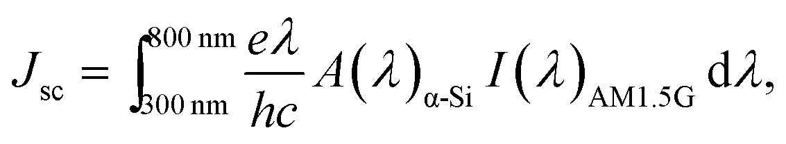
To evaluate the performance of the designed solar cells, we have calculated in Fig. 1(c) the so-called integrated absorption 〈Aα-Si〉AM1.5G weighted by the air mass 1.5 global (AM1.5G) solar spectrum and the short circuit current density Jsc, as a function of the thickness t2. The physical quantity 〈Aα-Si〉AM1.5G is defined in the following expression:49,50
 | (1) |
 | (2) |
To further improve the absorption of the α-Si layer, arrays of Ag nanodisks are added to the solar cells. The right insert in Fig. 2(a) schematically shows the building block of the redesigned solar cells in which Ag disks are placed on the top surface of the α-Si layer and are completely embedded into the ITO anti-reflection layer. The Ag disk has the diameter d = 40 nm, height h = 12 nm, and the periods px = py = 65 nm. The thicknesses of the α-Si and ITO layers are kept invariable. Compared to the case of identical geometric parameters but without Ag disk (the left insert), the absorption of the α-Si layer is enhanced greatly for wavelengths between 740 and 800 nm, due to the excitation of the third absorption peak centered at 770 nm. Furthermore, the absorption around the FPα-Si resonance of 640 nm is also noticeably enhanced, with the peak value increased from 0.4 to 0.7. This effect is possibly because the metal disks aid in the impedance matching of the surface impedance of the solar cells with the impedance of free space.51 For wavelengths smaller than 480 nm, the absorption becomes a little weaker. Overall, the absorption in the α-Si layer is improved significantly after adding Ag disks, as clearly seen in Fig. 2(a). By adding arrays of Ag nanodisks into the solar cells, the integrated absorption 〈Aα-Si〉AM1.5G (the short circuit current density Jsc) is increased from 41% (10.1 mA cm−2) to 51% (13.4 mA cm−2). If Joule heat dissipated in the Ag disk and substrate is also included, the absorption can exceed 90% near the resonance wavelengths of 680 nm, as exhibited by the green triangles in Fig. 2(a). Such a high absorption case is commonly called “perfect absorption” that has been intensively studied in plasmonic metamaterial absorbers in recent years.32,33
 | ||
| Fig. 2 (a) Normal-incidence absorption spectra of only α-Si (red circles), and of both α-Si and Ag (green triangles) in the solar cells (right insert), with the thicknesses of α-Si and ITO layers t1 = 20 nm and t2 = 30 nm, the diameter and height of Ag disk d = 40 nm and h = 12 nm, and the period px = py = 65 nm. The absorption spectra (black squares) in the case without Ag disk (left insert), are shown again for comparison. (b) Current density distributions on the xoz plane across the center of Ag disk at the magnetic resonance of λ = 770 nm in (a), with incident electric field Ein set to be 1.0 V m−1 and polarized alone the x axis. Red arrows represent the current directions, gray dash lines outline the boundaries between different material regions, and green signs “+” and “−” stand for positive and negative charges, respectively. | ||
To unveil the physical mechanism of the third absorption peak at the wavelength of 770 nm, the current intensity distributions are plotted in Fig. 2(b) on the xoz plane across the center of Ag disk. It is clearly seen that the currents are mainly distributed in the Ag disk and its vicinity, with the maximum current intensity concentrated around the bottom edge of Ag disk. Red arrows overlaid in Fig. 2(b) indicate the current directions. According to the current directions, we can deduce the antisymmetric charge distributions on the edge of Ag disk and on the surface of Ag substrate, as indicated by green signs “+” and “−” in Fig. 2(b), which stand for positive and negative charges, respectively. The charge distributions correspond to the excitation of a resonance mode that can induce a magnetic dipolar moment counteracting the external magnetic field and produce diamagnetic responses. This type of resonance is usually termed magnetic resonance to differentiate it from a common plasmon resonance observed in metallic nanoparticles, and has been widely utilized to construct optical metamaterials with a negative refractive index.52,53 The formation of such a magnetic resonance can be well understood through plasmon hybridization between the Ag disk and substrate, similar to the case of metallic nanosandwiches.54
In order to better understand the properties of the magnetic resonance, in Fig. 3 we plot the electric and magnetic field distributions at the resonance wavelength of λ = 770 nm. The electric fields are mainly concentrated near the edge of Ag disk, and two hotspots on the left and right sides extend into the α-Si layer and reach to the top surface of Ag substrate [see Fig. 3(a) and (b)]. The magnetic fields are highly confined within the α-Si layer and have a maximum under the Ag disk [see Fig. 3(c) and (d)]. The field enhancements in the α-Si layer lead to the significantly improved light absorption around the magnetic resonance. The distribution properties of electromagnetic fields are typical characteristics of magnetic resonances,54,55 and are also similar to those in a paper that reported high-performance metamaterial absorbers based on magnetic resonances.38
 | ||
| Fig. 3 Normalized electric field E/Ein (left column) and magnetic field H/Hin (right column) distributions at the magnetic resonance of λ = 770 nm in Fig. 2(a) on the xoz plane (top row) across the center of Ag disk and the xy plane of z = 10 nm (bottom row) across the center of α-Si film. Incident field Ein is polarized alone the x axis. White lines plotted in (a) and (c) outline the boundaries between different material regions. | ||
Here we should mention that, a recently published work presented a similar design with metal nanodisks but on a thicker α-Si layer of about 400 nm, in which the plasmonic near-field effect of metal nanodisks was employed primarily for impedance tuning to excite strong different-order FP resonances in the thicker α-Si layer and thus enhance light absorption over a broad spectral range.51 Another similar work reported 90 nm-thick α-Si solar cells with one-dimensional silver grating embedded in an anti-reflection layer, in which multiple FP resonances in the anti-reflection and α-Si layers were combined with grating-coupling guided modes in the α-Si layer to obtain efficient solar harvesting.56 In our work, the α-Si layer is so thin (only 20 nm) that the near-field plasmon interactions between the Ag disk and substrate are strong enough to form an antisymmetric hybridized mode (i.e., magnetic dipolar resonance). We take full advantage of the magnetic resonance and two lowest-order FP resonances in the ITO and α-Si layers for high light absorption.
In the following, we will investigate in detail the effects of several geometric parameters on the performance of solar cells schematically shown by the right insert in Fig. 2(a). We first investigate the effects of the array period and the height h of Ag disks. For this purpose, Fig. 4(a) shows the contour plot of normal-incidence absorption of α-Si thin film as a function of the period and the incident wavelength. The period gradually increases from 45 to 80 nm while the other geometric parameters are kept the same as those in Fig. 2(a). In this plot, the absorption bands resulting from the FPα-Si and FPITO resonances and the magnetic resonance (MR) are labeled as “FPα-Si”, “FPITO” and “MR”, respectively. When the period increases, two FP resonances do not move noticeably since the thicknesses of the ITO and α-Si layers are unchanged. However, their excitation strength depends strongly on the period, and there exists an optimum period for the maximized light absorption. The magnetic resonance blue-shifts very quickly at first and then slowly, because of the dramatic change in the near-field plasmon interactions between Ag disks in the close proximity. For larger periods, the interactions between Ag disks become very weak, so the position of the magnetic resonance is almost independent of the period. The properties make the magnetic resonance different from the well-known waveguide modes which always red-shift with the increasing period of coupling grating.56Fig. 4(b) shows the contour plot of normal-incidence absorption of α-Si thin film as a function of the incident wavelength and the height h of Ag disks. It is easily found that the absorption bands of two FP resonances almost stay as the height h varies. But, the larger h is, the weaker are the FPITO absorption band, since increasing h will lead to a higher reflection owing to higher metallic filling ratio. In contrast, the FPα-Si absorption band becomes much stronger, maybe because the geometric skin depth reduction of metals minimizes ohmic losses in metallic nanostructures despite higher metallic filling ratio.44 As h increases, the absorption band of the magnetic resonance gets stronger and stronger, and reaches a maximum for h = 14 nm.
 | ||
| Fig. 4 Contour plots of normal-incidence absorption spectra of α-Si film, for the period px and py increased from 45 to 80 nm in steps of 5 nm (a), and for the height h of Ag disks increased from 7 to 16 nm in steps of 1 nm (b). The other geometric parameters are the same as those in Fig. 2(a). The absorption bands resulting from two FP resonances and a magnetic resonance are labeled as “FPα-Si”, “FPITO” and “MR”, respectively. Solar-spectrum weighted absorption 〈Aα-Si〉AM1.5G and short circuit current density Jsc as a function of the period (c) and the height h (d). | ||
From the above two plots, the corresponding solar-spectrum weighted absorption 〈Aα-Si〉AM1.5G and short circuit current density Jsc are calculated by eqn (1) and (2), and are presented in Fig. 4(c) and (d). The two physical quantities will quickly increase at first and reach a maximum as the period varies from 45 to 65 nm, then decline gradually and finally approach the limit values in the case of no Ag disk, with the period increased further. When h becomes larger, both 〈Aα-Si〉AM1.5G and Jsc will also increase firstly and then decrease. Their maxima can reach nearly 51% and 13.4 mA cm−2 under an optimal situation in which the height h is 12 nm and the period is about 65 nm. A recently proposed metamaterial-plasmonic solar cell with a checkerboard-patterned top metallic layer and an extremely thin 15 nm α-Si active layer was simulated to exhibit good performance with Jsc of 19.7 mA cm−2,45 compared with 16.8 mA cm−2 from the highest-efficiency α-Si solar cells so far.57
The effect of the diameter d of Ag disk on the performance of solar cells is shown in Fig. 5(a), which presents the contour plots of normal-incidence absorption spectra of α-Si thin film for d increased from 20 to 60 nm in steps of 5 nm. The other geometric parameters are the same as those in Fig. 2(a). When the diameter d gets larger, the absorption band labeled as “MR” will noticeably shift upward as a whole because of a red-shift of the magnetic resonance, and at the same time the light absorption strength becomes much weaker due to the continuously decreasing imaginary part of the permittivity for α-Si. The absorption band attributed to FPITO resonance has no dramatic change in position since the thicknesses of the ITO thin film is unvaried, and its strength decreases continuously mostly because the increasing metallic filling ratio enhances the reflection of incident light. The absorption band of FPα-Si resonance will blue-shift for a larger d, with its strength increasing gradually to a maximum for d = 55 nm. Fig. 5(b) exhibits the diameter dependence of solar-spectrum weighted absorption 〈Aα-Si〉AM1.5G and short circuit current density Jsc. With increasing d, 〈Aα-Si〉AM1.5G and Jsc will quickly increase at first, reaching their maxima for d = 40 nm. As d is further increased, however, the two physical qualities will decrease dramatically, partly because the magnetic resonance red-shifts away from the wavelength range between 400 and 700 nm in which the photon flux density of the AM1.5G solar spectrum I(λ)AM1.5G is pronounced, and simultaneously the absorption at the magnetic resonance is greatly reduced, as clearly demonstrated in Fig. 5(c). Another reason is that the FPITO absorption band is weakened continuously with the increasing d, as just discussed above.
 | ||
| Fig. 5 (a) Contour plots of normal-incidence absorption spectra of α-Si thin film for the diameter of Ag disk d increased from 20 to 60 nm in steps of 5 nm. The other geometric parameters are the same as those in Fig. 2(a). (b) Solar-spectrum weighted absorption 〈Aα-Si〉AM1.5G and short circuit current density Jsc as a function of d. (c) Normal-incidence absorption spectra of α-Si thin film for three diameters of 30, 40, and 50 nm. The photon flux density of the AM1.5G solar spectrum, I(λ) AM1.5G, is also shown for discussion purposes. | ||
Next, we investigate the effect of the thickness t1 of the α-Si thin film on the performance of solar cells. Fig. 6(a) presents a contour plot of normal-incidence absorption spectra of α-Si thin film, in which the thickness t1 is varied from 10 to 40 nm in steps of 2 nm, while the other geometric parameters are the same as those in Fig. 2(a). The absorption band resulting from the magnetic resonance has an evident enhancement and reaches its maximum when t1 increases to about 30 nm, and then decreases gradually as t1 increases further. This property is qualitatively consistent with a previous work which demonstrated perfect absorption from Joule heat at a magnetic resonance in metamaterial absorbers.38 Meanwhile, the magnetic resonance is continuously broadened in bandwidth, and finally almost merges with the red-shifted FPα-Si resonance. With increasing t1, the FPITO resonance shows no change in position since the thickness of ITO layer is fixed, and its corresponding light absorption has also no noticeable change. In contrast, the FPα-Si resonance noticeably red-shifts out of the spectral region between 500 and 700 nm in which I(λ)AM1.5G is high, and its corresponding light absorption decreases gradually. The effect of increasing t1 on the solar-spectrum weighted absorption 〈Aα-Si〉AM1.5G and short circuit current density Jsc are shown in Fig. 6(b). As t1 increases to about 14 nm, both 〈Aα-Si〉AM1.5G and Jsc will saturate, with their maxima being 55% and 14.1 mA cm−2, respectively. However, they will significantly decrease as t1 increases further. Here, we should mention that 〈Aα-Si〉AM1.5G and Jsc are very sensitive t1, which are reduced from their maxima of 55% and 14.1 mA cm−2 for t1 = 14 nm, to 35% and 8.4 mA cm−2 for t1 = 40 nm. In order to obtain the optimum performance of the designed solar cells, precisely control of the thickness of the active layer is very important.
 | ||
| Fig. 6 (a) Contour plot of normal-incidence absorption spectra of α-Si thin film, with the thickness t1 of α-Si film varied from 10 to 40 nm in steps of 2 nm. The other geometric parameters are the same as those in Fig. 2(a). (b) Solar-spectrum weighted absorption 〈Aα-Si〉AM1.5G and short circuit current density Jsc as a function of the thickness t1. | ||
We have also investigated the effect of light incident angle θ on the absorption for both P and S polarizations, which are shown in Fig. 7(a) and (b), respectively. For S polarization with incident electric field Ein parallel to the xoy plane, three absorption bands in Fig. 7(b) are gradually weakened in strength when θ varies from 0° to 80°, although their positions remain almost unchanged. As a result, the corresponding solar-spectrum weighted absorption 〈Aα-Si〉AM1.5G and short circuit current density Jsc decline slowly with the increasing θ, as exhibited by the red triangles in Fig. 7(c) and (d). For P polarization with the incident magnetic field Hin parallel to the xoy plane, two absorption bands in Fig. 7(a) ascribed to the FPITO and the magnetic resonance are also gradually weakened in strength for the increasing θ, with their positions almost unchanged. On the contrary, the absorption band of the FPα-Si resonance becomes stronger after 50°, maybe owing to the existence of electric field component perpendicular to the xoy plane for P polarization. Also, its position has an evident blue shift when θ is varied from 50° to 80°. Therefore, differing from the case of S polarization, both 〈Aα-Si〉AM1.5G and Jsc will not reduce but rather grow a little bit until θ increases up to about 70°. For further increased θ, they will also reduce but more slowly compared to the S polarization case. On the whole, the two physical quantities are less dependent of the incident angle and polarization of light when θ is smaller than 20°, but decline obviously after 70° and 20° for P and S polarizations, respectively. Since sun light is not polarized, we also plot the curves for unpolarized light, which are produced as an average over the results of both polarizations. Additionally, the position of the magnetic resonance is almost independent of θ for both polarizations, which is distinct from guide modes propagating within a thicker α-Si layer whose resonance wavelengths are very sensitive to incident angle (i.e., red-shifts quickly with increasing θ) because their excitations are via grating coupling.56
 | ||
| Fig. 7 (a) Contour plots of normal-incidence absorption spectra of α-Si thin film in the solar cells shown by the right insert in Fig. 2(a) with incidence angle θ increased from 0 to 80 degrees in steps of 5 degrees, for P polarization (a) and S polarization (b) with incident electric field Ein and magnetic field Hin parallel to the xoy plane, respectively. The geometric parameters are the same as those in Fig. 2(a). Solar-spectrum weighted absorption 〈Aα-Si〉AM1.5G (c) and short circuit current density Jsc (d) as a function of θ for both P and S polarizations, and for unpolarized incident light as well. | ||
Finally, we would like to discuss the problem of overestimation of Jsc and experimental implementation of the proposed solar cells. In the semiconductor layers, the absorbed photons owing to the existence of bulk defects are commonly considered as loss through electron–hole recombination, which will not contribute to the photocurrent. Due to the interruption of the lattice arrangements on the semiconductor surfaces, there are also surface defects (i.e., generate dangling bonds at surface), which can cause very high electron–hole recombination rate. The surface and volume electron–hole recombinations are unavoidable, but in eqn (2) all generated electron–hole pairs are supposed to contribute to the photocurrent, so the values of Jsc calculated by this equation are always overestimated. An efficient way to reduce dangling bonds is to grow a thin dielectric film (like Al2O3 and SiO2) on the semiconductor surfaces, that is, surface passivation. Improving the surface passivation quality to decrease the surface recombination has become one of most effective methods for high photovoltaic conversion efficiency. The dangling bonds can also be terminated on hydrogen atoms to improve the performance of α-Si thin film. Our design includes very small Ag nanodisks with diameters from 20 to 60 nm, and Fig. 5(b) shows that Jsc is very sensitive to the size of Ag nanodisks. Therefore, it is vital to accurately control the disk size to obtain maximal Jsc. If there is a deviation of −10 nm from the optimum diameter of 40 nm, the value of Jsc will be reduced from 13.4 to 12.8 mA cm−2 by 4.5%. Advanced but expensive nanofabrication techniques like electron beam lithography (EBL) could be utilized to integrate such small nanostructures into the solar cells. Additionally, standard α-Si solar cells have a p–i–n junction with α-Si thickness in the order of several hundred nanometers,58–60 which is not easy to fit into 20 nm. This may be realized with the help of sophisticated doping technology (e.g., ion implantation), employed to make metal–oxide–semiconductor field-effect transistor (MOSFET) in the semiconductor industry. Fast developed 3D printing maybe provide an alternative approach to fabricate the proposed solar cells in the future. At present, extrusion-based 3D printing has been utilized to fabricate quantum dot-based light emitting diodes (QD-LEDs) that exhibit pure and tunable color emission properties.61 Metal organic chemical vapor deposition (MOCVD) is also possibly able to grow a 20 nm-thick p–i–n junction. In fact, it has been used to grow a highly Si-doped n-GaN layer of only 10 nm in multi-junction solar cells.62 Despite some experimental challenges, we hope that the numerical results presented in this work could guide the design of resonant structures for optimized ultrathin solar cells.
4. Conclusions
In conclusion, we have theoretically studied thin-film solar cells composed of an ITO-covered ultrathin α-Si film on Ag substrate, with a square array of Ag disks placed on the top surface of the α-Si film and completely embedded within the ITO anti-reflection layer. The effects of all geometric parameters including the thicknesses of ITO and α-Si layers, the height and diameter of Ag disk, and the array period, on the performance of the solar cells have been investigated in detail. It is found that an ultrathin α-Si film of only 20 nm thickness is able to absorb over 50% solar energy in the spectral range from 300 to 800 nm at normal incidence, and the amount of absorbed light is equivalent to photocurrent of about 13.4 mA cm−2, after the geometric parameters are optimized. This is attained by the excitations of two lowest-order FP resonances in the α-Si and ITO layer and a magnetic resonance originating from plasmon hybridization between the Ag disk and substrate. It is also found that the absorption efficiency of this α-Si film is less dependent on the incident angle and polarization of light for incident angles smaller than 20°, but it will decrease dramatically after 70° and 20° for P and S polarizations, respectively.Acknowledgements
This work is financially supported by the State Key Program for Basic Research of China (SKPBRC) under Grant No. 2013CB632703 and 2012CB921501, the National Natural Science Foundation of China (NSFC) under Grant No. 11104136, 11104135, 11304159, 51172105, 91221206, and 51271092, the Natural Science Foundation of Zhejiang Province under Grant No. LY14A040004, the Specialized Research Fund for the Doctoral Program of Higher Education of China under Grant No. 20133223120006, and the Scientific Research Foundation of Nanjing University of Posts and Telecommunications under Grant No. NY213023.Notes and references
- J. Zhao, A. Wang, M. A. Green and F. Ferrazza, Appl. Phys. Lett., 1998, 73, 1991 CrossRef CAS PubMed.
- W. Shockley and H. J. Queisser, J. Appl. Phys., 1961, 32, 510 CrossRef CAS PubMed.
- A. V. Shah, H. Schade, M. Vanecek, J. Meier, E. Vallat-Sauvain, N. Wyrsch, U. Kroll, C. Droz and J. Bailat, Prog. Photovoltaics, 2004, 12, 113 CAS.
- M. A. Green, J. Zhao, A. Wang and S. R. Wenham, IEEE Trans. Electron Devices, 1999, 46, 1940 CrossRef CAS.
- S. Sandhu, Z. Yu and S. Fan, Opt. Express, 2013, 21, 1209 CrossRef CAS PubMed.
- G. Kang, H. Park, D. Shin, S. Baek, M. Choi, D. H. Yu, K. Kim and W. J. Padilla, Adv. Mater., 2013, 25, 2617 CrossRef CAS PubMed.
- J. Zhu, C. M. Hsu, Z. F. Yu, S. H. Fan and Y. Cui, Nano Lett., 2010, 10, 1979 CrossRef CAS PubMed.
- H. A. Atwater and A. Polman, Nat. Mater., 2010, 9, 205 CrossRef CAS PubMed.
- S. B. Mallick, N. P. Sergeant, M. Agrawal, J. Y. Lee and P. Peumans, MRS Bull., 2011, 36, 453 CrossRef CAS.
- K. R. Catchpole, S. Mokkapati, F. Beck, E. C. Wang, A. McKinley, A. Basch and J. Lee, MRS Bull., 2011, 36, 461 CrossRef CAS.
- M. A. Green and S. Pillai, Nat. Photonics, 2012, 6, 130 CrossRef CAS PubMed.
- C. H. Chou and F. C. Chen, Nanoscale, 2014, 6, 8444 RSC.
- C. F. Guo, T. Y. Sun, F. Cao, Q. Liu and Z. F. Ren, Light: Sci. Appl., 2014, 3, e161 CrossRef PubMed.
- C. Clavero, Nat. Photonics, 2014, 8, 95 CrossRef CAS PubMed.
- W. L. Barnes, A. Dereux and T. E. Ebbesen, Nature, 2003, 424, 824 CrossRef CAS PubMed.
- L. Zhang, J. M. Hao, H. P. Ye, S. P. Yeo, M. Qiu, S. Zouhdi and C. W. Qiu, Nanoscale, 2013, 5, 3373 RSC.
- X. Chen, Y. T. Chen, J. Dai, M. Yan, D. Zhao, Q. Li and M. Qiu, Nanoscale, 2014, 6, 1756 RSC.
- M. L. Brongersma, Y. Cui and S. H. Fan, Nat. Mater., 2014, 13, 451 CrossRef CAS PubMed.
- F. Priolo, T. Gregorkiewicz, M. Galli and T. F. Krauss, Nat. Nanotechnol., 2014, 9, 19 CrossRef CAS PubMed.
- L. Cao, J. S. White, J. S. Park, J. A. Schuller, B. M. Clemens and M. L. Brongersma, Nat. Mater., 2009, 8, 643 CrossRef CAS PubMed.
- K. Seo, M. Wober, P. Steinvurzel, E. Schonbrun, Y. Dan, T. Ellenbogen and K. B. Crozier, Nano Lett., 2011, 11, 1851 CrossRef CAS PubMed.
- A. B. Evlyukhin, S. M. Novikov, U. Zywietz, R. L. Eriksen, C. Reinhardt, S. I. Bozhevolnyi and B. N. Chichkov, Nano Lett., 2012, 12, 3749 CrossRef CAS PubMed.
- A. Vasudev, J. A. Schuller and M. L. Brongersma, Opt. Express, 2012, 20, A385 CrossRef CAS.
- P. Spinelli, M. A. Verschuuren and A. Polman, Nat. Commun., 2012, 3, 692 CrossRef CAS PubMed.
- J. Grandidier, D. M. Callahan, J. N. Munday and H. A. Atwater, Adv. Mater., 2011, 23, 1272 CrossRef CAS PubMed.
- O. Berger, D. Inns and A. G. Aberle, Sol. Energy Mater. Sol. Cells, 2007, 91, 1215 CrossRef CAS PubMed.
- L. Zeng, P. Bermel, Y. Yi, B. A. Alamariu, K. A. Broderick, J. Liu, C. Hong, X. Duan, J. Joannopoulos and L. C. Kimerling, Appl. Phys. Lett., 2008, 93, 221105 CrossRef PubMed.
- E. Garnett and P. Yang, Nano Lett., 2010, 10, 1082 CrossRef CAS PubMed.
- K. X. Wang, Z. Yu, V. Liu, Y. Cui and S. Fan, Nano Lett., 2012, 12, 1616 CrossRef CAS PubMed.
- A. Mavrokefalos, S. E. Han, S. Yerci, M. S. Branham and G. Chen, Nano Lett., 2012, 12, 2792 CrossRef CAS PubMed.
- Y. Yao, J. Yao, V. K. Narasimhan, Z. C. Ruan, C. Xie, S. H. Fan and Y. Cui, Nat. Commun., 2012, 3, 664 CrossRef PubMed.
- C. M. Watts, X. L. Liu and W. J. Padilla, Adv. Mater., 2012, 24, OP98 CAS.
- Y. X. Cui, Y. R. He, Y. Jin, F. Ding, L. Yang, Y. Q. Ye, S. M. Zhong, Y. Y. Lin and S. L. He, Laser Photonics Rev., 2014, 8, 495 CrossRef CAS PubMed.
- N. I. Landy, S. Sajuyigbe, J. J. Mock, D. R. Smith and W. J. Padilla, Phys. Rev. Lett., 2008, 100, 207402 CrossRef CAS.
- H. Tao, N. I. Landy, C. M. Bingham, X. Zhang, R. D. Averitt and W. J. Padilla, Opt. Express, 2008, 16, 7181 CrossRef.
- Y. Avitzour, Y. A. Urzhumov and G. Shvets, Phys. Rev. B: Condens. Matter Mater. Phys., 2008, 79, 045131 CrossRef.
- X. Liu, T. Starr, A. F. Starr and W. J. Padilla, Phys. Rev. Lett., 2010, 104, 207403 CrossRef.
- J. Hao, J. Wang, X. Liu, W. J. Padilla, L. Zhou and M. Qiu, Appl. Phys. Lett., 2010, 96, 251104 CrossRef PubMed.
- K. Aydin, V. E. Ferry, R. M. Briggs and H. A. Atwater, Nat. Commun., 2011, 2, 517 CrossRef PubMed.
- B. Zhu, J. Zhao, C. Huang and T. Jiang, Appl. Phys. Lett., 2010, 97, 051906 CrossRef PubMed.
- H. Tao, C. M. Bingham, A. C. Strikwerda, D. Pilon, D. Shrekenhamer, N. I. Landy, K. Fan, X. Zhang, W. J. Padilla and R. D. Averitt, Phys. Rev. B: Condens. Matter Mater. Phys., 2008, 78, 241103 CrossRef.
- Q. Y. Wen, H. W. Zhang, Y. S. Xie, Q. H. Yang and Y. L. Liu, Appl. Phys. Lett., 2009, 95, 241111 CrossRef PubMed.
- N. I. Landy, C. M. Bingham, T. Tyler, N. Jokerst, D. R. Smith and W. J. Padilla, Phys. Rev. B: Condens. Matter Mater. Phys., 2009, 79, 125104 CrossRef.
- A. Vora, J. Gwamuri, N. Pala, A. Kulkarni, J. M. Pearce and D. O. Guney, Sci. Rep., 2014, 4, 4901 CAS.
- Y. Wang, T. Y. Sun, T. Paudel, Y. Zhang, Z. F. Ren and K. Kempa, Nano Lett., 2012, 12, 440 CrossRef CAS PubMed.
- Data for α-Si and ITO: Sopralab basic n&k files database.
- E. D. Palik, Handbook of Optical Constants of Solids, Academic Press, 1985 Search PubMed.
- S. Fahr, C. Rockstuhl and F. Lederer, Phys. Rev. B: Condens. Matter Mater. Phys., 2013, 88, 115403 CrossRef.
- L. Zhou, X. Q. Yu and J. Zhu, Nano Lett., 2014, 14, 1093 CrossRef CAS PubMed.
- K. Q. Le and S. John, Opt. Express, 2014, 22, A1 CrossRef PubMed.
- A. Vora, G. Gwamuri, J. M. Pearce, P. L. Bergstrom and D. O. Guney, J. Appl. Phys., 2014, 116, 093103 CrossRef PubMed.
- G. Dolling, C. Enkrich, M. Wegener, J. F. Zhou, C. M. Soukoulis and S. Linden, Opt. Lett., 2005, 30, 3198 CrossRef CAS.
- V. M. Shalaev, W. Cai, U. K. Chettiar, H. K. Yuan, A. K. Sarychev, V. P. Drachev and A. V. Kildishev, Opt. Lett., 2005, 30, 3356 CrossRef.
- T. Pakizeh, M. S. Abrishamian, N. Granpayeh, A. Dmitriev and M. Käll, Opt. Express, 2006, 14, 8240 CrossRef CAS.
- C. J. Tang, P. Zhan, Z. S. Cao, J. Pan, Z. Chen and Z. L. Wang, Phys. Rev. B: Condens. Matter Mater. Phys., 2011, 83, 041402(R) CrossRef.
- I. Massiot, C. Colin, C. Sauvan, P. Lalanne, P. R. I. Cabarrocas, J. L. Pelouard and S. Collin, Opt. Express, 2013, 21, A372 CrossRef CAS PubMed.
- M. A. Green, K. Emery, Y. Hishikawa, W. Warta and E. D. Dunlop, Prog. Photovoltaics, 2014, 22, 701 Search PubMed.
- W. S. Yan and M. Gu, J. Opt., 2014, 16, 045003 CrossRef.
- V. E. Ferry, M. A. Verschuuren, H. B. T. Li, E. Verhagen, R. J. Walters, R. E. I. Schropp, H. A. Atwater and A. Polman, Opt. Express, 2010, 18, A237 CrossRef CAS PubMed.
- J. D. Winans, C. Hungerford, K. Shome, L. J. Rothberg and P. M. Fauchet, Opt. Express, 2015, 23, A92 CrossRef PubMed.
- Y. L. Kong, I. A. Tamargo, H. Kim, B. N. Johnson, M. K. Gupta, T. W. Koh, H. A. Chin, D. A. Steingart, B. P. Rand and M. C. McAlpine, Nano Lett., 2014, 14, 7017 CrossRef CAS PubMed.
- N. G. Young, E. E. Perl, R. M. Farrell, M. Iza, S. Keller, J. E. Bowers, S. Nakamura, S. P. DenBaars and J. S. Speck, Appl. Phys. Lett., 2014, 104, 163902 CrossRef PubMed.
Footnote |
| † These authors contributed equally to this work. |
| This journal is © The Royal Society of Chemistry 2015 |