DOI:
10.1039/C5RA17148B
(Paper)
RSC Adv., 2015,
5, 78192-78208
Intriguing properties of unusual silicon nanocrystals†
Received
25th August 2015
, Accepted 7th September 2015
First published on 7th September 2015
Abstract
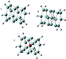
Solar cell technologies are highly dependent on silicon materials and novel nanoclusters with optimal electronic properties. Based on a recent study on ultrastable silicon nanoclusters, an analysis of the effects of modifications of those nanocrystals by carboxylation, amidation, hydroxylation and halogenation has been performed using quantum mechanical methods of study. Here we report the gaps, electronic structures, absorption spectra, and effects on the charge-transfer potential of a collection of modified silicon nanoclusters. The results show that the pristine silicon clusters retain the highest charge-transfer properties and that halogenation impacts on the charge-transfer effects in a proportional fashion to the electronegativity of the employed halogens. Modification with organic molecules does not improve charge-transfer properties, and gives instead the highest reduction of charge-transfer potentials of the silicon clusters. The effects of the modification have also been studied in context with the orbital configurations through wave function analysis, which reveals that the electrostatic properties of the nanoclusters are mainly represented by a significant polarization of the electrostatic energy between the peripheral regions of the clusters and their core, a feature particularly well-preserved in the pristine silicon clusters. Modifying the particles by adding an extra atom at their core shows significant effects on the molecular orbital properties (HOMO/LUMO). However, this modification does not contribute to an actual increase in charge-transfer integrals. The modifications induce, however, interesting effects on the overall configuration of the clusters; i.e., they increase the aromatic character of the inter-atomic bonding pattern. Halogenation has the highest effect on improving aromatic properties for the silicon clusters, where chlorination gives the highest degree of aromaticity. This study introduces valuable electronic data for engineering novel silicon nanoclusters for application in solar cell technologies, computing units, and other fields such as in aerospace engineering.
Introduction
Global energy resources are a key aspect of modernization and modern society developments. With the increasing use of technological and microelectronic solutions and consumables in society, global energy demands bring challenges to research in energy with sustainable and green technologies.1,2 In this context, solar cells and silicon based technologies represent a crucial point for the development of green and renewable energy solutions, with particular emphasis on photovoltaic cells, wafer technologies, polymer-based photocatalytic membranes and cells, and nanowires.3–7 Silicon is ubiquitous in nature, and exerts excellent semi-conductive, conductive and insulating properties in bulk materials. Moreover, in the form of nanocrystals and nanoclusters, silicon can be tuned to operate at higher conductivities than in bulk materials, and be also used for high-energy applications in combination with transition metals. Methods for synthesizing nano-sized silicon clusters are often based on plasma and ion beam techniques8,9 which permit to control the particle size and, thus, their band gaps. In addition, UV-emitting properties of these particles can be obtained in co-synthesized metallic nanoislands via the formation of plasmon-induced electric fields.9 Silicon nanocrystals and clusters can have very small band gaps,10 and be used as nanodots and quantum dots in photonics and microtechnologies.11–13 In addition, such clusters can be used for nanowire technologies, as they can exert a quantum confinement effect14 via their small diameters yielding a direct band gap that increases with decreasing nanowire diameter.15
Recent research on modifications of silicon clusters has shown that nanocluster size and morphology affect the quantum mechanical properties of the clusters.16 Also, halogenation of silica has shown improved interatomic potentials for silica ensembles,17 and nanoparticles of silica have been found to be excellent materials for conductive matrixes in relevant technologies such as nanosensors.18 The modifications of silica by halogenation can in other words be a very valuable avenue of research for the synthesis of novel nanocrystals, as halogens retain particular electronic properties (i.e. high electronegativity, low ionization potentials) given lower nuclear shielding effects on their valence electrons.
The development of new silica-based and silicon-based technologies relies, however, on accurate and sound predictions for nanocrystals, where quantum mechanical studies represent an indispensable resource in the prediction of properties for molecular and electronic ensembles of crystals, lattices and atomistic units.16,19–21 With the use of quantum mechanics, electronic properties such as charge-transfer potentials,22 electron delocalization,21 bond metallicity,23 electron localization,24 aromaticity,25 electronic gaps are generated, functioning directly as a basis for the structuring and synthesis of nanomaterials and nanocrystals.
One example of those promising new silicon materials is presented by over-coordinated hydrogenated silicon clusters as the Si19H12 nanocrystal.21 This entity is composed of three parallel, planar hexagons with one additional Si atom close to the cluster center causing its hypervalent and electron-deficient character. In principle, all ring structures suffer from more or less strain. Due to the electron-deficient nature of the Si19H12 nanocrystal, however, the traditional approach to estimate strain energies based on homodesmotic reactions26 might lead to completely erroneous results.27 Based on both ab initio molecular dynamics (AIMD) simulations and recent experimental measurements, it has been demonstrated that the associated ring strain in the Si19H12 nanocrystal is completely negligible due to the high degree of electron deficiency in the atomic bonds.27 In an earlier study, it had actually been shown that the electron deficiency induces extensive electron delocalization that causes those clusters to be ultrastable and to possess aromatic-like properties.28 We like to remind here that “ultrastable” does not necessarily mean global minimum energy structure, but rather that the electron deficiency induces strong electron delocalization that leads to non tetrahedral entities that are more stable than their tetrahedral counterparts. Consequently, the use of those nontetrahedral nanocrystals for the fabrication of nanodevices in realistic plasma reactors has been predicted.29
In this context, the present study reports on an extensive quantum chemical study of a series of modifications on hydrogenated silicon nanoclusters, with additional insertion of one Si or one Ge atom close to the center of the selected Si18X12 nanostructures, where X = F, Cl, Br, NH2, COOH, and OH. The different properties, including geometries, absorption spectra, electronic structures, reactivities, charge-transfer integrals, and other critical features of the electronic properties are used to study the effects on the modified clusters.
The results from this study supply valuable information for the further development of novel energy technologies and report key features of the electronic effects for chemically modified silicon nanoclusters with different sizes and morphologies and elucidate the effects at the electronic structure level.
Materials and methods
Choice of structures
All structures and modifications (see next paragraph) resulted in a diameter class of approximately 1 nm. The origin of these structures is from an earlier work by Vach21 based on the self-assembly dynamics during the nucleation process in realistic low-temperature and low-pressure plasma-reactor synthesis.28–30 Given the low-diameter size of these nanoparticles, their use and application is expected to be as nano-colloids, suspensions or as crystals. These can be applied in solar technologies via suitable routes of manufacturing. Parts of this manufacturing process can be carried out via methods from Greene and colleagues on ZnO nanorods at start-dimensions of 5 nm.31 If successfully synthesized, the experimental electronic properties derived for this selection of structures are expected to be coherent with the data derived throughout this text and is restricted to the given dimensions. Larger particle classes must be explored in a separate study and require additional investigation. The authors chose furthermore to investigate hexagonal structures of silicon, as those from ref. 28–30 because of their potential presence of over-coordinated states from the abovementioned synthesis method by plasma-reactors. The hexagonal structures are therefore of interest to the authors for modification effects by passivization.
Gaussian calculations
All structures were prepared in Gaussian 09 rev. A.01 (ref. 32) and optimized using the B3LYP functional33 with the 6-31G(d) basis set.34 A set of structures encompassed a C6h cluster of 18 silicon atoms arranged in a hexagonal crystal system (Fig. 1A). Another two sets of clusters were modeled by introducing either an additional silicon or germanium atom close to the center of the 18 silicon atom structure of the first set (Fig. 1B and C). Each of the nanostructures was subjected to modifications of their peripheral hydrogens, replacing these by selected halogens (Br, Cl and F), and NH2, COOH, and OH groups. The latter two modifications were added to investigate the effects of oxygen atoms on the nanocluster electronic structures. Optimization calculations of those structures were carried out to find the optimized minima on the potential energy surface. Frequency calculations did not show any imaginary frequencies for the optimized molecules.
 |
| | Fig. 1 Optimized structures of A: empty Si18H12Si NCs arranged in a C6h symmetry of hexagonal crystal geometry; B: Si19H12, the 19th Si atom situated in the center of the lattice structure, C: Si18GeH12, Ge atom situated in the center of the lattice structure. | |
Average local ionization energies
The average local ionization energy, Ī(r), is interpreted as a means of estimating the sites of the more reactive electrons in a molecule or cluster and is given by:35,36| |
 | (1) |
where ρi(r) is the electronic density of the ith occupied atomic or molecular orbital and εi, the energy of ith orbital, is its focus being upon the point in space rather than upon a particular orbital. The computed Ī(r) is evaluated on the molecular surface and labeled ĪS(r). The minima of ĪS(r), ĪS,min, correspond to the least tightly-held electrons, which should be the most reactive sites to electrophilic or free radical attack.35,36
Optical absorption spectra
Optical absorption spectra were calculated using time-dependent density-functional theory (TD-DFT) implemented in the Gaussian09 package.32 Minimum energy structures of all investigated clusters were employed as configurations for the TD-DFT calculations. The hybrid, non-local exchange and correlation functional of Becke, Lee, Parr, and Yang (B3LYP) and the 6-31G(d) basis set were used. The validity of this basis set was verified by having performed several calculations with the 6-311++G(d,p) basis set that gave essentially the same results. For each structure, 150 singlet excited states were computed for the absorption spectra.
Wavefunction and NICS analyses
Natural population analysis (NPA) was conducted using the NBO3.1 module embedded in the Gaussian 09 package.32 Density of states analysis, orbital interaction diagram analysis, quantitative analysis of electrostatic potential on vdW surfaces, atoms in molecules (AIM) analysis, Mayer and Laplacian bond order calculations, as well as electron localization function (ELF) analysis were all performed using Multiwfn 3.3.6.37 Nucleus-independent chemical shifts (NICS) were calculated with Gaussian 09.32 All wavefunction analyses were based on B3LYP/6-31G* wavefunctions, while NICS analysis was carried out at B3LYP/6-31+G* level.
Charge-transfer properties
The calculation of the charge-transfer integrals is carried out through solving the electronic coupling, V, between two molecules of the same species, such as two Si19H12 molecules for instance. The results are presented in Table 4. The methods is carried out according to ref. 38 and resolves the equation: V = (J − S(ε1 − ε2)/2)/(1 − S2). Here, J is the interaction integral, defining the level of interaction between the nucleus and the electron density on the neighbor nucleus, S is the overlap integral and the epsilons are the eigenvalues of energies of each fragment under consideration (HOMO-for n-type transfer, and LUMO for p-type transfer). The charge-transfer integrals were calculated using the Amsterdam Density Functional (ADF) package,39,40 with the PW91 method at the triple-zeta level with polarization functions (TZP).34,41 The approach relies first on solving the single point state for each modified nanocluster deriving from the Gaussian calculations (vide supra), which was subsequently considered as a fragment in the paired nanocluster calculations (pairs of identical clusters) (Fig. 2). All modified single clusters were subjected to an enforced symmetry imposition. The symmetry tolerance was set to 10−10 Å on all coordinates for the single nanocluster calculations. Non-halogenated clusters were subjected to geometry optimization with the PW91 method before pair-wise calculations. The pair-wise calculations of the modified clusters were carried by a single-point calculation with enforced symmetry of pairs (Fig. 2). The inter-cluster distance was defined by 2.9 Å between each symmetrically aligned halogen pair, after a careful evaluation of a series of non-covalent bond lengths. The symmetry tolerance was set to 0.1 Å for the pair-wise calculations. The method for solving the charge-transfer integrals is described in the ADF manual.39 The Si19H12 clusters were arranged in a D6h and C2v symmetry manually, without using the “symmetrize” function in ADF. The distance was set as above, to 2.9 Å between two separate hydrogen atoms. Subsequently, the two Si19H12 pairs were subjected to a geometry optimization with the PW91 method. The finalized outputs were then subjected to charge-transfer calculations, via the approach described above and in the ADF manual.39
 |
| | Fig. 2 Symmetry for pairs of clusters for the charge-transfer study. Each cluster was arranged co-axially to the other central axis in a D6h symmetry (top) and perpendicularly in a C2v symmetry (bottom). The nanoclusters with halogens were set at a distance between the halogen atoms (example above: fluorine atoms) of 2.9 Å before optimization. Groups with compatible polar interactions (COOH, NH2, and OH) were set at an initial distance of 2.5 Å. Pristine Si-clusters were set at an initial distance of 2.5 Å between the hydrogen atoms. | |
Results and discussion
Orbital and gap analyses
The empty Si18H12 and the endohedrally filled Si19H12 and Si18GeH12 silicon nanocrystals (Si NCs) were optimized at a B3LYP/6-31 G(d) level of theory and the HOMO–LUMO gaps are shown in Fig. 3. The geometry optimizations were performed without any symmetry constraints. In some endohedrally filled Si NCs, the inserted Si or Ge atoms deviate from the center of the cluster by 0.03–0.38 Å (Table 1). The temporal periodic change of this distance was the subject of a parallel investigation for the Si19H12 nanocrystal.29 One of the effects caused by the 19th atom can be seen in the energy change between the highest occupied molecular orbital EHOMO and the lowest unoccupied molecular orbital ELUMO (Table 1). Table 1 shows that the narrowest HOMO–LUMO gaps are found for silicon clusters where the 19th atom is close to the core with a most favorable modification of the peripherical atoms by hydrogenation and hydroxylation (Table 1, Fig. 3). In general, the HOMO–LUMO gap decreases from the empty Si18X12 to the filled Si19X12 and Si18GeX12 crystals. The effect of reduced gap width of the clusters with 19 lattice atoms, compared to 18-atom clusters is caused by the electronic configuration difference between Ge and Si which results in a nearly 30% expansion of the HOMO–LUMO gaps when the former is applied for the halogenated variants. This large difference results from the existence of the 3d electrons of germanium which induce a strong electron–electron repulsion below the valence shell of germanium, compared to the less electron-populated 3s orbital of silicon. The result of the presence of the fully occupied 3d orbital in germanium is a lower shielding effect on the valence electrons of germanium, than the 3s induce on the 3p electrons of silicon. The reduced shielding effect arising from stronger electron–electron repulsions in the 3d orbitals of germanium contributes in making the valence electrons less stable between the Ge and Si atoms, expanding the HOMO–LUMO gap.
 |
| | Fig. 3 The HOMO–LUMO gap ΔE (eV) of studied silicon nanoclusters calculated at the B3LYP/6-31G(d) level of theory. | |
Table 1 The calculated first frequencies, HOMO and LUMO energies, HOMO–LUMO band gaps, dipole moment, and distance of central Si/Ge from center of the studied Si NICs
| Cluster |
First frequency |
EHOMO (a.u.) |
ELUMO (a.u.) |
ΔE (eV) |
Dipole moment |
Distance from center (Å) |
| Si18H12 |
102.9 |
−0.2081 |
−0.1198 |
2.403 |
0.0005 |
— |
| Si19H12 |
88.5 |
−0.1698 |
−0.1123 |
1.565 |
1.1429 |
0.27 |
| Si18GeH12 |
29.2 |
−0.1713 |
−0.1124 |
1.600 |
0.5691 |
0.15 |
| Si18F12 |
59.4 |
−0.2412 |
−0.1392 |
2.775 |
0.0001 |
— |
| Si19F12 |
56.2 |
−0.1929 |
−0.1292 |
1.731 |
0.0093 |
0.00 |
| Si18GeF12 |
68.8 |
−0.1939 |
−0.1297 |
1.747 |
0.0017 |
0.00 |
| Si18Cl12 |
46.4 |
−0.2476 |
−0.1508 |
2.632 |
0.0003 |
— |
| Si19Cl12 |
40.6 |
−0.2053 |
−0.1440 |
1.666 |
0.0044 |
0.00 |
| Si18GeCl12 |
49.7 |
−0.2057 |
−0.1446 |
1.662 |
0.0015 |
0.00 |
| Si18Br12 |
27.6 |
−0.2342 |
−0.1400 |
2.564 |
0.0001 |
— |
| Si19Br12 |
34.2 |
−0.1929 |
−0.1334 |
1.617 |
0.1090 |
0.23 |
| Si18GeBr12 |
33.3 |
−0.1939 |
−0.1334 |
1.646 |
0.0215 |
0.00 |
| Si18(COOH)12 |
10.4 |
−0.2208 |
−0.1310 |
2.443 |
2.3151 |
— |
| Si19(COOH)12 |
10.5 |
−0.1857 |
−0.1271 |
1.594 |
1.7221 |
0.12 |
| Si18Ge(COOH)12 |
12.1 |
−0.1870 |
−0.1274 |
1.621 |
2.0335 |
0.00 |
| Si18(NH2)12 |
53.1 |
−0.1524 |
−0.0582 |
2.557 |
0.0839 |
— |
| Si19(NH2)12 |
50.3 |
−0.1223 |
−0.0582 |
1.743 |
2.2696 |
0.38 |
| Si18Ge(NH2)12 |
28.8 |
−0.1163 |
−0.0533 |
1.713 |
1.3193 |
0.15 |
| Si18(OH)12 |
52.9 |
−0.1912 |
−0.0920 |
2.700 |
0.0027 |
— |
| Si19(OH)12 |
25.8 |
−0.1419 |
−0.0856 |
1.531 |
0.0951 |
0.03 |
| Si18Ge(OH)12 |
64.4 |
−0.1429 |
−0.0859 |
1.549 |
0.0162 |
0.00 |
The effects on the electronic gaps by halogenation display an electronic behavior which leads to the expansion of the excitation gaps. Interestingly enough, when comparing the 19-atom clusters to the 18-atom clusters (ΔE18 − ΔE19), the more the halogen is changed from Br > Cl > F, the larger the decrease of the overall excitation gap is. A fluorinated cluster of 19 atoms compared to a fluorinated cluster of 18 atoms has the largest change in gap (1.044 eV), followed by 0.966 eV for chlorine and 0.947 eV for bromine. This intriguing effect shows that the core silicon atom in the 19 atom clusters has a central role in the conductive pattern of the clusters. This effect on the 19 atom clusters is potentially affected by the ionization potential within the silicon cluster itself, as the increasing levels of electron-negativity (Fe.n. = 4.0, Cle.n. = 3.0, Bre.n. = 2.8) mainly affect the ionization energies of the inter-atomic valence electrons. The aminated, carboxylated and hydroxylated groups has minor effects on the HOMO–LUMO gaps of the nanoclusters (Table 1, Fig. 3), however, the –OH modifications gave a larger impact on the Si18 structures than on the Si19. This is expected to be caused by the effect of the 19th silicon atom, which is described in the section concerning the wavefunction analysis. The effects of the other modifications are also reported further during the wavefunction analysis.
Average local ionization energies
A local property that has often been used in relation with surface reactivity is the average local ionization energy, defined by eqn (1). Fig. 4 shows the ĪS(r) plotted on the ρ = 0.001 a.u. molecular surface for Si18H12 and Si19H12. It is seen that silicon itself has very reactive electrons, as depicted by the relatively low ĪS,min values. The lowest ĪS,min are associated with the middle-layer silicon atoms; these ĪS,min have values of about 7.4 eV (Table 1). These sites, thus, correspond to the least tightly-held electrons, which should be the most reactive sites to electrophilic or to free radical attack. It is evident from Table 2 that the magnitude of the ĪS,min associated with the silicon atoms depends upon the electron-withdrawing/donating power of the X group. Also apparent is that the presence of electron-donating groups (NH2 and OH) results in lower ĪS,min values while the electron-withdrawing COOH substituent leads to higher ĪS,min values. Table 2 shows also another interesting feature, where the ĪS,min values of the systems tend to increase as the size of the substituted halogen increases, which implies a decreasing effect on the ionization energy by the electronegativity of the halogen. In other words, the halogens give an increase in average ionization potential and higher chemical stabilization of the silicon nanoparticles.
 |
| | Fig. 4 Computed average local ionization energy ĪS(r) on the 0.001 a.u. molecular surface of Si18H12 (a) and Si19H12 (b). Color ranges in eV: red > 9.3, yellow 8.4–9.3, green 7.5–8.4, blue < 7.5. Light blue circles denote the positions of the ĪS(r) minima, the ĪS,min. | |
Table 2 Computed ĪS(r) minima, the ĪS,min for all investigated systems
| System |
ĪS,min (eV) |
| Si18H12 |
7.4 |
| Si18F12 |
8.2 |
| Si18Cl12 |
8.5 |
| Si18Br12 |
8.6 |
| Si18(COOH)12 |
8.4 |
| Si18(OH)12 |
6.8 |
| Si18(NH2)12 |
6.6 |
| Si19H12 |
6.6 |
| Si19F12 |
7.5 |
| Si19Cl12 |
7.6 |
| Si19Br12 |
7.7 |
| Si19(COOH)12 |
7.1 |
| Si19(OH)12 |
6.0 |
| Si19(NH2)12 |
5.9 |
| Si18GeH12 |
7.2 |
| Si18GeF12 |
8.1 |
| Si18GeCl12 |
8.3 |
| Si18GeBr12 |
8.1 |
| Si18Ge(COOH)12 |
8.2 |
| Si18Ge(OH)12 |
6.6 |
| Si18Ge(NH2)12 |
6.5 |
As discussed in an earlier work,21 electron delocalization in electron-deficient hydrogenated silicon Si19H12 nanocrystals leads to the induction of an aromatic-like behavior of the electrons, yielding a higher degree of electron sharing among the cage atoms. This may also affect the average local ionization energies associated with silicon atoms. As a result of this electron delocalization, we show in Fig. 4b that the ĪS(r) values on the side of the Si19H12 nanostructure are quite different than those of the Si18H12 one. We find ĪS,min to be 6.6 eV for Si19H12, leading to an approximated activation of 0.8 eV. Comparison with the ĪS,min of Si18H12 indicates that the surface reactivity of the nanocrystal is clearly modified after the Si or Ge insertion. What is especially notable is the significant reduction in ĪS,min for the insertion of a silicon atom. The results reveal that the silicon insertion tends to activate the surface toward electrophilic/radical attack. Such a different reactivity pattern between the Si18H12 and Si19H12 can be attributed to the delocalization of p-electrons that are delocalized between the center silicon atom and its neighbors. Table 2 reveals that the insertion of the center Ge atom also tends to activate the Si18H12 surface toward electrophilic/radical attack, although the effect is weaker than for Si insertion. This is most likely due to the different charge transfer effects between the inserted atom and Si18H12, which will be discussed in the following and to the lower ionization energy of germanium in its elemental form (7.8994 eV) compared to silicon (8.1517 eV).
Absorption spectra
Maximum absorption wavelengths, oscillator strengths, and molar absorption coefficients of all investigated clusters in the IR, VIS, and UV regions are summarized in Table 3. All Si19X12 (with X = H, Br, Cl, F, COOH, NH2, and OH) and Si18GeX12 clusters can absorb light in the three spectral regions, whereas none of the Si18X12 clusters exhibits absorption in the IR. The Si18H12 cluster can only absorb in the UV. Those results are consistent with the absorption spectra calculations for Si19H12 and Si18H12 clusters using TD-DFT/6-311++G(d,p).21 The extension of the absorption spectra of Si19X12 and Si18GeX12 clusters up to the IR is assigned to the insertion of the central over-coordinated Si or Ge atoms. The role of endohedral atoms (Si or Ge); i.e., with over-coordinated Si or Ge atoms, on the ability of nanocrystals to absorb in the VIS and IR can be definitively demonstrated when comparing with SinHn−1M clusters (with M = H, Cl, and F; n = 20, 24, 26, and 28)42 which have no over-coordinated Si atoms and display absorption strictly limited to the UV region. This observation especially holds for the tetrahedral silicon fullerene Si20H20 that has quite the same size of about 1 nm. In general, standard tetrahedral hydrogenated silicon clusters of this size show absorption only in the UV and may absorb light in the VIS and IR only when toxic or expensive metal groups (as PbS, PbSe, CdS, CdSe, Au, or Cr) are incorporated into them.43–52 The wide absorption spectral range of the investigated Si19X12 and Si18GeX12 clusters might open immediate applications in the most various fields, for instance, photovoltaic devices and cancer treatment.21
Table 3 Maximum absorption wavelengths (λmax), oscillator strengths (f), and molar absorption coefficients (εmax) of all investigated clusters computed with TD-DFT/6-31G(d) in the IR, VIS, and UV regions
| Structure |
IR |
VIS |
UV |
| λmax (nm) |
f |
εmax (M−1 cm−1) |
λmax (nm) |
f |
εmax (M−1 cm−1) |
λmax (nm) |
f |
εmax (M−1 cm−1) |
| Si19H12 |
814.61 |
0.0234 |
1872.00 |
411.49 |
0.0146 |
1168.00 |
295.44 |
0.0947 |
7576.00 |
| Si19Br12 |
1006.04 |
0.0398 |
4643.33 |
437.95 |
0.0148 |
1726.66 |
293.72 |
0.1015 |
11 841.67 |
| Si19Cl12 |
956.86 |
0.041 |
4100.00 |
445.08 |
0.0133 |
1330.00 |
281.75 |
0.1247 |
12 470.00 |
| Si19F12 |
894.17 |
0.0356 |
2136.00 |
420.11 |
0.0096 |
576.00 |
275.37 |
0.1822 |
10 932.00 |
| Si19(COOH)12 |
934.22 |
0.0323 |
7177.78 |
439.71 |
0.0063 |
1400.00 |
356.08 |
0.0421 |
9355.56 |
| Si19(NH2)12 |
800.72 |
0.0300 |
6000.00 |
534.30 |
0.0129 |
2580.00 |
317.74 |
0.0722 |
14 440.00 |
| Si19(OH)12 |
894.04 |
0.0373 |
1790.40 |
461.73 |
0.0153 |
734.40 |
292.89 |
0.2221 |
10 660.80 |
| Si18GeH12 |
881.23 |
0.0276 |
3154.29 |
413.64 |
0.0061 |
697.14 |
295.20 |
0.0673 |
7691.43 |
| Si18GeBr12 |
976.5 |
0.0417 |
4170.00 |
501.36 |
0.0188 |
1880.00 |
292.28 |
0.1302 |
13 020.00 |
| Si18GeCl12 |
964.59 |
0.0385 |
3300.00 |
487.33 |
0.0174 |
1491.43 |
309.04 |
0.1277 |
10 945.71 |
| Si18GeF12 |
892.13 |
0.0336 |
2240.00 |
458.41 |
0.0142 |
946.67 |
274.39 |
0.1671 |
11 140.00 |
| Si18Ge(COOH)12 |
995.05 |
0.0414 |
2957.14 |
412.26 |
0.0354 |
2528.57 |
334.64 |
0.1229 |
8778.57 |
| Si18Ge(NH2)12 |
904.11 |
0.0388 |
5432.00 |
486.00 |
0.0159 |
2226.00 |
320.62 |
0.0909 |
12 726.00 |
| Si18Ge(OH)12 |
891.63 |
0.0356 |
1708.80 |
507.91 |
0.0195 |
936.00 |
292.78 |
0.2126 |
10 204.80 |
| Si18H12 |
|
|
|
|
|
|
262.30 |
0.0988 |
8892.00 |
| Si18Br12 |
|
|
|
406.58 |
0.0074 |
575.56 |
277.19 |
0.1645 |
12 794.44 |
| Si18Cl12 |
|
|
|
403.65 |
0.0060 |
360.00 |
270.04 |
0.1989 |
11 934.00 |
| Si18F12 |
|
|
|
406.65 |
0.0031 |
241.11 |
257.93 |
0.1662 |
12 926.67 |
| Si18(COOH)12 |
|
|
|
400.96 |
0.0055 |
2200.00 |
378.14 |
0.0310 |
12 400.00 |
| Si18(NH2)12 |
|
|
|
403.21 |
0.0159 |
3180.00 |
284.65 |
0.0966 |
19 320.00 |
| Si18(OH)12 |
|
|
|
433.55 |
0.0026 |
156.00 |
270.36 |
0.2642 |
15 852.00 |
Charge-transfer integrals
Charge-transfer integrals report the energy necessary for a charge transfer to take place between two or several molecules. As aforementioned, high values indicate non-optimal charge-transfer, while low values indicate optimal charge-transfer.
Charge-transfer integrals are valuable to estimate the efficiency of molecules or nanoclusters as conductive units in electronic devices such as field-effect transistors, photovoltaic cells, light-emitting diodes, nanophotonic devices, nanowires, nanoarrays, and other similar structures. Charges conducted across a material or a set of molecules move either in p-modes (hole-to-hole) or n-modes (occupied orbital to occupied orbital). Charge-transfer integrals are useful in determining the optimal mode of the conductive operation of the materials, and can be used to estimate the most feasible mode of electronic operation of the material in an electronic operation mode, in surface coating materials, components in nano-devices, or as crystalline units in solar cell wafers.
The charge-transfer integrals are shown in Table 4, where the charge-transfer values for the two main geometries C2v and D6h of each cluster pair are also reported in a summed total for simplicity of interpreting the results. The cluster with optimal charge transfer integrals, both in p- and n-mode of operation is the native Si18H12 cluster proposed by Vach and colleagues.21 The insertion of a 19th silicon atom at the core has a reductive effect on the charge-transfer integrals for the pristine Si–H cluster, affecting in particular its p-type mode of operation integral. All modifications result in a reduction of charge-transfer potential, with emphasis on COOH and NH2, as well as OH. This effect is caused by the electron-withdrawing effects that nitrogen and oxygen have on the carbon atoms that would otherwise be bonded to hydrogens. A second cause of this is the electronic repulsion that arises between oxygen groups of two nanoparticles next to one another. This repulsion is likely to affect the charge-transfer potential. Electronic analysis of paired clusters has not been performed given our present limitations in computational time; however, a set of new electronic studies of pairs of clusters can confirm these observations further. The halogenated modifications preserve still a significant charge-transfer potential, compared to the organic-modified clusters. Insertion of a germanium atom at the core has improving effects primarily for the substitution with NH2 in p-type operation and OH-clusters; however it does not improve the charge-transfer effective potential of the pristine Si18H12. In general, the modified nanoclusters with 19 silicon atoms display more optimal charge-conducing characteristics compared to the 18-silicon atom clusters, particularly for Cl, Br and F. When comparing the three Si19-halogenated states, the electronegativity of the halogen is critical to modulate the charge-transfer integral, where fluorine with an electronegativity of 4.0 shows the least reducing effects on Jeff in p-mode of charge-transfer, followed by bromine and chlorine (Table 4). These patterns are not equally well-preserved for the halogenated clusters comprised of 18 silicon atoms, which interestingly, give a better conductive potential in n-mode of operation than the halogenated clusters with 19 silicon atoms. The employed symmetric arrangement of cluster pairs has the highest effect accounting for most clusters. The optimal charge-transfer potential is obtained when the nanoclusters are arranged in a D6h symmetry, rather than C2v improving most of the charge-transfer properties in n-type operation. This observation is quite crucial and depends on the linear arrangement of the modification groups, in the D6h symmetry, all modifications are aligned with maximum interaction surfaces to one another. In a C2v symmetry, the modifications are disaligned, and have low contact surfaces (Fig. 2).
Table 4 Charge-transfer properties of the modified silicon nanoclusters. All integrals have to be negative to yield favorable charge-transfer mobility. Fragment energies depict the energies of each molecule in a charge-transfer pair. Jeffp: effective charge-transfer integral (p-mode); Jeffn: effective charge-transfer integral (n-mode). Symmetry types: for “H” “horizontal” (C1) and “P” for “perpendicular” (C1), see respectively D6h and C2v orientations in Fig. 2. The non-halogen groups disallow symmetries, however the silicon grids of the two respective non-halogenated nanoparticles are aligned respectively to D6h and C2v
| Cluster pairs |
Symmetry |
HOMO fragments energy (eV) |
LUMO fragments energy (eV) |
Jeffp-mode (eV) |
Jeffn-mode (eV) |
| ε1 |
ε2 |
ε1 |
ε2 |
| Si18H12 × 2 |
D6h |
−5.536 |
−5.536 |
−4.881 |
−4.881 |
−0.340 |
−0.550 |
| Si18H12 × 2 |
C2v |
−5.229 |
−5.597 |
−4.635 |
−4.307 |
−0.097 |
−0.034 |
| ∑: |
|
|
|
|
|
−0.437 |
−0.584 |
| Si19H12 × 2 |
D6h |
−4.783 |
−4.783 |
−3.761 |
−3.761 |
0.052 |
−0.145 |
| Si19H12 × 2 |
C2v |
−4.752 |
−4.870 |
−3.683 |
−3.841 |
0 |
0.002 |
| ∑: |
|
|
|
|
|
0.052 |
−0.143 |
| Si18GeH12 × 2 |
D6h |
−4.687 |
−4.687 |
−3.787 |
−3.787 |
0.051 |
−0.139 |
| Si18GeH12 × 2 |
C2v |
−4.629 |
−4.778 |
−3.710 |
−3.874 |
0 |
0 |
| ∑: |
|
|
|
|
|
−0.051 |
−0.139 |
| Si18F12 × 2 |
D6h |
−7.610 |
−7.610 |
−6.145 |
−6.145 |
0.065 |
−0.218 |
| Si18F12 × 2 |
C2v |
−7.622 |
−7.514 |
−6.083 |
−6.018 |
0.002 |
−0.056 |
| ∑: |
|
|
|
|
|
0.067 |
−0.274 |
| Si19F12 × 2 |
D6h |
−5.449 |
−5.449 |
−4.486 |
−4.488 |
−0.140 |
0 |
| Si19F12 × 2 |
C2v |
−5.553 |
−5.348 |
−4.597 |
−4.441 |
−0.018 |
0 |
| ∑: |
|
|
|
|
|
−0.158 |
0 |
| Si18GeF12 × 2 |
C2v |
−5.564 |
−5.371 |
−4.695 |
−4.557 |
−0.036 |
−0.018 |
| Si18GeF12 × 2 |
D2h |
−5.467 |
−5.467 |
−4.652 |
−4.652 |
−0.016 |
−0.073 |
| ∑: |
|
|
|
|
|
−0.052 |
−0.091 |
| Si18Cl12 × 2 |
D6h |
−6.418 |
−6.418 |
−5.032 |
−5.032 |
0.050 |
−0.103 |
| Si18Cl12 × 2 |
C2v |
−6.423 |
−6.407 |
−5.024 |
−5.004 |
0 |
0.002 |
| ∑: |
|
|
|
|
|
−0.050 |
−0.101 |
| Si19Cl12 × 2 |
D6h |
−5.730 |
−5.730 |
−4.706 |
−4.706 |
−0.114 |
−0.078 |
| Si19Cl12 × 2 |
C2v |
−5.885 |
−5.660 |
−4.784 |
−4.649 |
0.012 |
0.010 |
| ∑: |
|
|
|
|
|
−0.102 |
−0.068 |
| Si18GeCl12 × 2 |
D6h |
−5.715 |
−5.715 |
−4.700 |
−4.700 |
−0.125 |
−0.090 |
| Si18GeCl12 × 2 |
C2v |
−5.781 |
−5.641 |
−4.777 |
−4.653 |
0.008 |
0.002 |
| ∑: |
|
|
|
|
|
−0.117 |
−0.088 |
| Si18Br12 × 2 |
D6h |
−6.277 |
−6.277 |
−4.941 |
−4.941 |
0.087 |
−0.104 |
| Si18Br12 × 2 |
C2v |
−6.270 |
−6.284 |
−4.922 |
−4.911 |
0.052 |
0.0028 |
| ∑: |
|
|
|
|
|
0.139 |
−0.076 |
| Si19Br12 × 2 |
D6h |
−5.640 |
−5.640 |
−4.557 |
−4.557 |
−0.134 |
−0.017 |
| Si19Br12 × 2 |
C2v |
−5.740 |
−5.543 |
−4.644 |
−4.532 |
0.030 |
0 |
| ∑: |
|
|
|
|
|
−0.104 |
−0.017 |
| Si18GeBr12 × 2 |
D6h |
−5.719 |
−5.719 |
−4.720 |
−4.720 |
−0.133 |
−0.090 |
| Si18GeBr12 × 2 |
C2v |
−5.691 |
−5.692 |
−4.717 |
−4.720 |
−0.014 |
−0.001 |
| ∑: |
|
|
|
|
|
−0.147 |
−0.091 |
| Si18(COOH)12 × 2 |
H |
−5.849 |
−5.947 |
−4.587 |
−4.685 |
−0.018 |
−0.009 |
| Si18(COOH)12 × 2 |
P |
−5.877 |
−5.885 |
−4.638 |
−4.635 |
0 |
−0.002 |
| ∑: |
|
|
|
|
|
−0.018 |
−0.011 |
| Si19(COOH)12 × 2 |
H |
−5.196 |
−5.184 |
−4.387 |
−4.376 |
−0.007 |
0 |
| Si19(COOH)12 × 2 |
P |
−5.189 |
−5.239 |
−4.370 |
−4.433 |
0.001 |
−0.008 |
| ∑: |
|
|
|
|
|
−0.006 |
−0.008 |
| Si18Ge(COOH)12 × 2 |
H |
−5.165 |
−5.190 |
−4.400 |
−4.317 |
−0.001 |
−0.004 |
| Si18Ge(COOH)12 × 2 |
P |
−5.229 |
−5.097 |
−4.467 |
−4.338 |
−0.003 |
0.001 |
| ∑: |
|
|
|
|
|
−0.004 |
−0.003 |
| Si18(NH2)12 × 2 |
D6h |
−4.098 |
−4.098 |
−2.520 |
−2.520 |
0.024 |
−0.060 |
| Si18(NH2)12 × 2 |
C2v |
−4.046 |
−4.258 |
−2.479 |
−2.674 |
0.012 |
−0.002 |
| ∑: |
|
|
|
|
|
0.036 |
−0.062 |
| Si19(NH2)12 × 2 |
C2 |
−3.336 |
−3.357 |
−2.562 |
−2.576 |
−0.048 |
−0.002 |
| Si19(NH2)12 × 2 |
C1 |
−3.536 |
−3.284 |
−2.753 |
−2.485 |
−0.004 |
−0.002 |
| ∑: |
|
|
|
|
|
−0.052 |
−0.004 |
| Si18Ge(NH2)12 × 2 |
C2 (P) |
−3.362 |
−3.413 |
−2.519 |
−2.568 |
−0.069 |
−0.004 |
| Si18Ge(NH2)12 × 2 |
C2 (H) |
−3.326 |
−3.354 |
−2.499 |
−2.523 |
−0.059 |
0 |
| ∑: |
|
|
|
|
|
−0.128 |
−0.004 |
| Si18(OH)12 × 2 |
C2 |
−5.023 |
−4.855 |
−3.887 |
−3.715 |
0.009 |
0 |
| Si18(OH)12 × 2 |
D6h |
−4.895 |
−4.895 |
−3.764 |
−3.764 |
0.013 |
0.059 |
| ∑: |
|
|
|
|
|
0.022 |
0.059 |
| Si19(OH)12 × 2 |
C2 |
−4.265 |
−4.040 |
−3.492 |
−3.295 |
−0.007 |
−0.008 |
| Si19(OH)12 × 2 |
D6h |
−4.061 |
−4.061 |
−3.300 |
−3.300 |
−0.093 |
−0.002 |
| ∑: |
|
|
|
|
|
0.100 |
0.010 |
| Si18Ge(OH)12 × 2 |
C2 |
−4.180 |
−4.226 |
−3.468 |
−3.51 |
−0.011 |
−0.024 |
| Si18Ge(OH)12 × 2 |
D6h |
−4.135 |
−4.135 |
−3.425 |
−3.425 |
−0.069 |
−0.035 |
| ∑: |
|
|
|
|
|
−0.080 |
−0.049 |
Charge distribution
The nature of the X group and the inserted atom must have significant influences on the charge distribution of the Si18X12 clusters. In order to make this point clear, we calculated Natural Population Analysis (NPA) charges for the X groups, the peripheral silicon atoms (i.e. the ones linking to the X groups), the middle-layer silicon atoms and the inserted Si or Ge atoms; the results are listed in Table 5. From the table it can be seen that for all Si18X12, Si19X12 and Si18GeX12 clusters, the X groups possess clearly negative charges, while the peripheral silicon atoms possess large positive charges. This is mainly because silicon has such a small electronegativity (1.90), which is even smaller than hydrogen (2.10). From the charge of the X groups, it is clear that the order of electron-withdrawing ability is F > OH > NH2 > Cl > COOH > Br > H, and the charge variation trend of the peripheral silicon atoms is inversely correlated with it. In the case of the Si18X12, the middle-layer silicon atoms have more electrons than the peripheral ones and thus are negatively charged; however, no clear relationship is observed between their charges and the electron-withdrawing ability of the X groups. In both the Si19X12 and Si18GeX12, the charge of the middle-layer silicon atoms is close to zero, while that of the inserted Si or Ge is quite negative, ranging from ∼0.59 to ∼0.75 for Si and from ∼0.76 to ∼0.89 for Ge. It is worth noting that the insertion of an atom into the center of the Si18X12 cluster only weakly affects the charge of peripheral silicon atoms; conversely, the exchange of the X group does not only affect the charge of the silicon atoms directly linking to them, but also somewhat affects those beyond them (i.e. the middle-layer silicon atoms and the inserted atom). This phenomenon is somewhat expected, because insertion only brings one additional atom into the system, while exchange of the X group involves as many as 12 groups simultaneously and thus should impose relatively higher influence on the charge of the silicon atoms.
Table 5 NPA charges of the X groups (qX), peripheral silicon atoms (qSi-peri), middle-layer silicon atoms (qSi-mid) and the inserted atom (qins) of Si18X12, Si19X12 and Si18GeX12. The valence electron configurations of the inserted atoms are shown in the last column
| |
X group |
qX |
qSi-peri |
qSi-mid |
qins |
Ins. config.a |
| z denotes the direction of the symmetry axis of the clusters. Due to symmetry, px and py share the same occupation number and thus they are shown together. |
| Si18 |
H |
−0.122 |
0.199 |
−0.154 |
— |
— |
| F |
−0.608 |
0.770 |
−0.324 |
— |
— |
| Cl |
−0.336 |
0.430 |
−0.190 |
— |
— |
| Br |
−0.234 |
0.317 |
−0.167 |
— |
— |
| OH |
−0.569 |
0.727 |
−0.315 |
— |
— |
| NH2 |
−0.509 |
0.652 |
−0.287 |
— |
— |
| COOH |
−0.309 |
0.375 |
−0.134 |
— |
— |
| Si19 |
H |
−0.119 |
0.192 |
−0.006 |
−0.708 |
s1.18px/y1.01pz1.48 |
| F |
−0.610 |
0.728 |
−0.112 |
−0.747 |
s1.13px/y1.07pz1.45 |
| Cl |
−0.338 |
0.396 |
0.003 |
−0.710 |
s1.13px/y1.07pz1.42 |
| Br |
−0.236 |
0.287 |
0.011 |
−0.676 |
s1.16px/y1.06pz1.37 |
| OH |
−0.574 |
0.688 |
−0.115 |
−0.673 |
s1.12px/y1.05pz1.41 |
| NH2 |
−0.513 |
0.626 |
−0.128 |
−0.591 |
s1.21px/y1.01pz1.32 |
| COOH |
−0.317 |
0.356 |
0.043 |
−0.727 |
s1.11px/y1.04pz1.51 |
| Si18Ge |
H |
−0.127 |
0.184 |
0.024 |
−0.874 |
s1.23px/y1.04pz1.52 |
| F |
−0.610 |
0.729 |
−0.089 |
−0.893 |
s1.24px/y1.09pz1.43 |
| Cl |
−0.338 |
0.394 |
0.029 |
−0.845 |
s1.23px/y1.09pz1.40 |
| Br |
−0.237 |
0.283 |
0.046 |
−0.831 |
s1.23px/y1.09pz1.40 |
| OH |
−0.574 |
0.688 |
−0.093 |
−0.807 |
s1.23px/y1.07pz1.40 |
| NH2 |
−0.512 |
0.621 |
−0.092 |
−0.756 |
s1.24px/y1.04pz1.40 |
| COOH |
−0.318 |
0.355 |
0.072 |
−0.876 |
s1.20px/y1.06pz1.51 |
To further reveal the electronic structure characteristics of the inserted atoms, the configuration of their valence electrons were obtained via NPA analysis and are shown as the last column of Table 5. From the data one can see that there is no notable difference between the inserted Si and Ge in electronic configuration, and that the electron occupation number of the valence pz atomic orbital (the one parallel to the symmetry axis of the clusters) is clearly higher than that of the px and py atomic orbitals.
Density of states (DOS)
The chlorine halogenated Si18 is a representative nanocluster in the series of silicon clusters that will be subjected to a complete DOS analysis. To better understand how the Si or Ge insertion changes the molecular orbital energies and HOMO–LUMO gaps, we plotted the total density of states (TDOS) for Si19Cl12 and Si18GeCl12 in Fig. 5a. The partial densities of states (PDOS) of the inserted atoms are also shown so that their contribution to the TDOS can be evaluated. As a comparison, the TDOS of Si18Cl12 is plotted in Fig. 5b. From the graph, one can see that there is almost no difference between the Si insertion case and Ge insertion case in the DOS, both inserted species produce a new state into the forbidden region of Si18Cl12, and hence significantly narrow the HOMO–LUMO gap. This observation is in line with the earlier study of Si19H12.21 From orbital isosurfaces, we have found this new state is essentially the LUMO of Si18Cl12 (the peak at approx. −4 eV in Fig. 5b), the interaction between Si18Cl12 and the extra Si significantly shifts down the LUMO energy, and due to the additional electrons brought by the inserted Si, the LUMO finally becomes the HOMO.
 |
| | Fig. 5 (a) Total density of states (TDOS) and partial density of states (PDOS) maps for Si19Cl12 and Si18GeCl12, the purple arrow marks the new state due to the Si or Ge insertion; (b) TDOS map of Si18Cl12. The DOS value is in arbitrary units. Occupied state regions are shaded for clarity. A Gaussian function with full width at half maximum (FWHM) of 0.4 eV was used for broadening molecular orbital energies to yield the DOS curves. | |
We also calculated HOMO and LUMO compositions for all the silicon clusters studied herein to study their characteristics in detail (Table S1†). The table shows that for all cases, the HOMOs and especially the LUMOs, are primarily given from the Si18 skeleton; the contribution from the inserted atom is commonly small; only in the case of X = H, the contribution of the inserted atom to the HOMO is notable (23.5% for Si19H12 and 33.6% for Si18GeH12). No general relationship between the characteristics of the X group or of the inserted atom and the HOMO/LUMO composition can be found.
Orbital interaction analysis
Orbital interaction diagram analysis is a commonly used approach to study how fundamental MOs are mixed to form complex MOs. This analysis helps us in understanding the nature of the frontier MOs of the silicon clusters. The orbital interaction diagram of the representative Si19Cl12 is shown in Fig. 6, the Si18X12 cage and the inserted Si (in s2pz2 configuration) are respectively taken as the two fragments. As highlighted by the pink arrows in Fig. 6, due to the phase matching, the doubly degenerate HOMOs of Si18Cl12 substantially mix with the 3px and 3py virtual atomic orbitals of the inserted Si and yield two low-lying degenerate MOs of Si19Cl12. The blue arrows in Fig. 6 highlight that, since the LUMO+1 of the Si18Cl12 has the same orbital phase as the 3pz orbital of the inserted Si, they are strongly mixed and result in one of the (nearly) triply degenerate HOMO−1 of the Si19Cl12. The doubly degenerate LUMO of Si19Cl12 directly derives from the doubly degenerate LUMO+2 of Si18Cl12 (see grey arrow in Fig. 6). The most noteworthy MO is the HOMO of the Si19Cl12, which as mentioned above is crucial for lowering the gap of the Si18Cl12 cluster. As highlighted by the green arrows in Fig. 6, this orbital is essentially the LUMO of the Si18Cl12, but now occupied by two electrons and the energy is decreased by 0.7 eV. The 3s orbital of the inserted Si (−11.6 eV) and the 221th MO of the Si18Cl12 (−7.8 eV) also participate in the HOMO of Si19Cl12, but the amount can be neglected (1.4% and 5.4%, respectively).
 |
| | Fig. 6 Orbital interaction diagram for Si19Cl12. The inserted Si takes its s2pz2 configuration. Vertical axis shows MO energies in eV. Solid and dashed bars correspond to occupied and virtual MOs, respectively. The one and two gaps in the bars mean the corresponding states are doubly and triply degenerate, respectively. Some MOs are plotted as isosurface graphs with an isovalue of 0.03. The numbers marked beside the red lines indicate the contribution from the fragmental MO to the Si19Cl12 MOs. For clarity, the contributions close to 100% are not labeled, and those smaller than 10% are not highlighted by red lines. | |
In short, the orbital interaction diagram analysis clearly shows that due to the Si insertion, the characteristics of the frontier MOs of Si19Cl12 distinctly differ from the counterparts of Si18Cl12; as a result, the HOMO–LUMO gap narrows significantly. This observation also holds for other X groups and for the Ge insertion case.
Electrostatic potential analysis
Electrostatic potential (ESP) is a key function for studying and predicting intermolecular interactions and is commonly studied on molecular van der Waals (vdW) surfaces.53 An investigation on the ESP of the silicon clusters must be very helpful for revealing how the inserted atom and the X groups affect the interactions between the clusters and other chemical species. To intuitively capture the basic characteristics of the ESP distribution on the vdW surface of our series of silicon clusters, we first examine the ESP mapped vdW surface of the representative Si19Cl12. From Fig. 7, it can be seen that in the top and bottom (or two-ends) regions as well as in the equatorial region, the ESP is quite positive: the maximum value in the former and latter reaches +22.2 and +30.5 kcal mol−1, respectively, suggesting that the silicon atoms under these surfaces tend to be attacked by nucleophiles and prefer to bind to Lewis-bases by electrostatic attraction. The ESP on the surface covering the chlorines exhibits small negative values around −6.3 kcal mol−1, this observation is consistent with the atomic charge analysis (Table 5), which shows that the NPA charge of the chlorines is negative (−0.34). It is worth noting that at the terminal of each chlorine, there is a local maximum of ESP with a small positive value (+3.8 kcal mol−1), which is known as σ-hole and is the source of the well-known halogen bonds.53,54 In fact, the σ-hole is present in all the Si18X12, Si18GeX12 and Si19X12 clusters when X = Cl, Br.
 |
| | Fig. 7 Top view and side view of the electrostatic potential (ESP) mapped with the vdW surface of Si19Cl12. The ESP values are in kcal mol−1. The vdW surface is defined as the isosurface of ρ = 0.001 a.u. Yellow and cyan spheres correspond to the position of local maxima and minima of the ESP on the vdW surface, respectively. ESP values are labeled beside them. | |
It is difficult to graphically compare the ESP on vdW surfaces for all 21 clusters involved in our present work. However, from Fig. 7, we note that it is useful and reasonable to partition the whole vdW surface into three local regions, namely the equatorial region, the “two-ends” region and the X group region; then, it will be straight forward to compare them respectively. So, we employed the local molecular surface analysis function of the Multiwfn program to obtain the average ESP (referred to as
)55 in the three regions of the local vdW surfaces for all 21 clusters, the results are listed in Table 6. The partition manner is illustrated in Fig. S1.† Table 6 also contains the maximum and minimum values of the ESP over the whole vdW surface. From the table, we have four main findings:
Table 6 Average ESP values on the local vdW surface of the X group region (
X), the equatorial region (
equ) and the two-ends region (
end). The minimum and maximum values of the ESP (Vmin and Vmax) over the whole vdW surface are also shown
| |
X group |
X |
equ |
end |
Vmin |
Vmax |
| Si18 |
H |
1.45 |
3.27 |
11.63 |
−1.69 |
16.37 |
| F |
−1.39 |
17.93 |
33.57 |
−10.67 |
45.72 |
| Cl |
0.39 |
18.73 |
30.33 |
−5.35 |
41.30 |
| Br |
−0.05 |
13.05 |
23.65 |
−7.54 |
33.59 |
| OH |
2.22 |
−1.64 |
5.84 |
−21.57 |
45.42 |
| NH2 |
2.16 |
−15.10 |
−12.69 |
−36.27 |
28.68 |
| COOH |
−2.72 |
4.05 |
13.94 |
−32.41 |
51.87 |
| Si19 |
H |
0.27 |
8.45 |
4.47 |
−3.46 |
14.72 |
| F |
−2.50 |
24.00 |
22.11 |
−12.00 |
31.29 |
| Cl |
−0.07 |
25.69 |
19.73 |
−6.41 |
30.54 |
| Br |
−0.33 |
19.42 |
13.64 |
−9.73 |
25.59 |
| OH |
1.48 |
3.55 |
−2.40 |
−22.94 |
43.92 |
| NH2 |
1.40 |
−9.13 |
−20.16 |
−39.07 |
29.25 |
| COOH |
−3.01 |
10.03 |
5.75 |
−31.37 |
51.40 |
| Si18Ge |
H |
0.03 |
8.76 |
4.26 |
−2.75 |
13.53 |
| F |
−2.54 |
23.80 |
21.96 |
−12.04 |
31.24 |
| Cl |
−0.21 |
25.80 |
19.53 |
−6.71 |
30.28 |
| Br |
−0.47 |
20.10 |
13.38 |
−8.58 |
24.20 |
| OH |
1.44 |
3.56 |
−2.72 |
−22.75 |
43.61 |
| NH2 |
1.20 |
−10.62 |
−17.37 |
−34.61 |
27.69 |
| COOH |
−3.03 |
10.38 |
5.39 |
−31.78 |
50.56 |
(1) In the equatorial and the two-ends regions of any cluster, when X is a single atom, the
is positive and large, meaning that these areas in this situation are quite favorable for binding a negatively charged substance. When X = H or COOH, the
is still positive, but not so large. In the case of X = OH, and in particular X = NH2, mostly due to the influence of the electron-rich lone-pair of the oxygen and nitrogen atoms, the
in one of, or in both of the equatorial and two-ends regions becomes negative, and thus completely loses its ability to attract Lewis-bases electrostatically.
(2) For Si18X12, the
in the two-ends region is more positive than that in the equatorial region, while the situation is completely inversed in the cases of Si19X12 and Si18GeX12 (the ESP mapped vdW surface of Si18Cl12 is given in Fig. S2† and the interested reader can compare it with Fig. 7). This observation can at least partially be explained based on atomic charges; from Table 5, it can be seen that after inserting a Si or Ge atom into Si18X12, the charges of the middle-layer silicon atoms, which dominate the ESP in the equatorial region, become nearly zero.
(3) When X = OH, NH2, COOH, both the global ESP minimum and maximum on the vdW surface occur in the X group region. This phenomenon originates from the electron-rich lone pair of the oxygen and nitrogen atoms as well as the highly positively charged hydrogens. It is expected that the corresponding silicon clusters can easily form hydrogen bonds via these X groups. When X = H, F, Cl, Br, the global ESP minimum on the vdW surface always occurs around the X groups, while the global maximum one occurs in the equatorial region for Si19X12 and Si18GeX12, and in the two-ends region for Si18X12.
(4) The insertion of both a Si or a Ge atom into the Si18X12 cage greatly changes its ESP distribution on the vdW surface. The choice of the insertion atom, however, only has minor effects on the ESP profiles of the nanoclusters.
Bonding analysis
In this section we study bonds in the silicon clusters. Atoms in molecules (AIM)56 is a very powerful theory for the investigation of bonding interactions. In this theory, critical points are the positions where the gradient norm of the electron density ρ is zero, which can be further classified according to the sign of the eigenvalues of the Hessian matrix of ρ. Bond critical points (BCP) have two negative eigenvalues, it usually occurs between interacting atom pairs. The bond path is the trajectory emitted from a BCP by tracing the steepest ascent direction of ρ, it unambiguously characterizes the interacting path between atoms. All BCPs and bond paths in Si19Cl12, as well as the naming of the silicon atoms are shown in Fig. 8. From the figure one can see that the central silicon atom directly binds to all six surrounding silicon atoms. Bonding interactions are also clearly present between each pair of SiP–SiP, SiM–SiM and SiP–SiM. The detectable curvature of the SiP–SiM bond paths is noteworthy, which implies that due to the cage strain effect the bonding electrons are bulged outwards.
 |
| | Fig. 8 Bond paths (brown lines) and bond critical points (orange spheres) of Si19Cl12. The naming of the three kinds of silicon atoms are labeled. | |
Mayer bond order57 is a quantity frequently used to study multiplicity of bonds and compare strength of the same kind of bonds. To study the characteristics of the Si–Si and Si–Ge bonds and to reveal the influence of atomic insertion and of the chosen X group, we computed Mayer bond order for all Si–Si or Si–Ge bonds and listed them in Table 7. One first notes that the bond order of most listed bonds is smaller than 1.0, suggesting that, on the average, less than one pair of electrons is involved in each of these bonds. This observation is in line with ref. 21, which showed that most Si–Si bonds in Si19H12 are electron-deficient. From Table 7, it can be seen that the order of bonding strength in Si18X12 is SiM–SiM > SiM–SiP > SiP–SiP; however, after inserting a Si or Ge atom in the cluster center, this sequence is completely reversed: the SiP–SiP bond then becomes the strongest one and has higher bond order than before. One possible reason may be that due to the presence of the inserted atom, some electron densities are pushed toward the peripheral silicon atoms from the middle-layer silicon atoms strengthening thus the SiP–SiP bonds; this inference can be readily justified by our atomic charge analysis of above (Table 5). For Si19X12 and Si18GeX12, the bonding between the inserted atom and the middle-layer silicon atoms is weak, the corresponding bond order is merely about 0.35; however, since there are six SiM–SiC/Ge bonds in total, the inserted atom can still be stabilized by the Si18 cage. The bond order of all bonds, except for the ones directly related to the inserted atom, are rather insensitive to the element of the inserted atom. Regarding the influence of the X group, from Table 7, one can see that the strength of the SiP–SiP bonds obviously depends on the nature of the X group, the sequence is identical in all clusters, namely H ≫ COOH ≅ NH2 > OH > Br > Cl ≅ F. The reason is understandable, that is the hydrogen and fluorine atoms have the weakest and strongest capacity of attracting electrons from the peripheral silicon atoms, respectively, and thus in the former case, the peripheral silicon atoms are able to utilize more electrons to form bonds than in the latter case. The Laplacian bond order58 which is shown to be very reliable to reveal bonding strength, was also employed by us to study the bonds in these systems, and we found almost identical conclusion as above (data not shown).
Table 7 Mayer bond orders of all Si–Si and Si–Ge bonds in all 21 clusters
| |
X group |
SiP–SiP |
SiP–SiM |
SiM–SiM |
SiM–SiC/Ge |
| Si18 |
H |
0.816 |
0.841 |
0.860 |
— |
| F |
0.690 |
0.723 |
0.778 |
— |
| Cl |
0.690 |
0.767 |
0.798 |
— |
| Br |
0.715 |
0.780 |
0.785 |
— |
| OH |
0.751 |
0.713 |
0.790 |
— |
| NH2 |
0.786 |
0.756 |
0.825 |
— |
| COOH |
0.779 |
0.814 |
0.814 |
— |
| Si19 |
H |
0.864 |
0.678 |
0.556 |
0.347 |
| F |
0.719 |
0.565 |
0.478 |
0.313 |
| Cl |
0.726 |
0.602 |
0.510 |
0.319 |
| Br |
0.745 |
0.609 |
0.505 |
0.327 |
| OH |
0.781 |
0.548 |
0.489 |
0.331 |
| NH2 |
0.808 |
0.589 |
0.523 |
0.355 |
| COOH |
0.811 |
0.656 |
0.524 |
0.325 |
| Si18Ge |
H |
0.864 |
0.685 |
0.549 |
0.373 |
| F |
0.718 |
0.569 |
0.476 |
0.353 |
| Cl |
0.727 |
0.603 |
0.506 |
0.354 |
| Br |
0.750 |
0.611 |
0.495 |
0.356 |
| OH |
0.780 |
0.551 |
0.486 |
0.367 |
| NH2 |
0.795 |
0.603 |
0.515 |
0.379 |
| COOH |
0.812 |
0.657 |
0.519 |
0.354 |
The electron localization function is a very powerful tool to study electron localization and delocalization problems.24,59,60 The ELF values range from 0 to 1, the larger the ELF at a point, the higher the probability that electrons localize around it. ELF is able to fruitfully reveal electronic structure characteristics in chemical systems, such as atomic shells, covalent bonds, lone pairs, as well as electron delocalization channels.59,61 To further unveil the nature of the interaction between the inserted atom and the surrounding ones in the clusters, we plotted ELF maps in the plane through the middle-layer silicon atoms for Si18Cl12 and Si19Cl12 in Fig. 9. From the figure, one can see that there is a yellow circle around the central silicon atom, which directly corresponds to the electrons weakly and covalently shared by the central and middle-layer silicon atoms. It is also expected that the electrons are relatively easy to delocalize around the central silicon atom by passing through the yellow circular channel. Concerning the cost of formation of the SiM–SiC covalent interactions, it is seen from Fig. 9 that the degree of electron localization between SiM–SiM is markedly reduced, in other words, the electron delocalization is strongly enhanced. This observation is in line with the above Mayer bond order analysis. We also plotted an ELF map for Si18GeCl12 in Fig. S3,† the characteristics of its ELF pattern is similar with that of Si19Cl12.
 |
| | Fig. 9 ELF distribution in the plane through the middle-layer silicon atomsof Si18Cl12 (a) and Si19Cl12 (b). | |
Aromaticity
Aromaticity is an interesting theoretical property of the silicon clusters studied here and highly worthy to be investigated. The most popular index for measuring aromaticity is the Nucleus-Independent Chemical Shift (NICS)25 which denotes the negative of the isotropic magnetic shielding tensor. For cylindrical clusters, a more thorough way to characterize aromaticity may be plotting the NICS curve along the symmetry axis of the cluster. We did this for all clusters involved in our present investigation. The results for the representative Si19Cl12 and Si18GeCl12, as well as all Si18X12 clusters are shown in Fig. 10; the NICS curve of benzene is also given in Fig. 10a for comparison. From Fig. 10a, it can be seen that Si18Cl12 does not show any evident aromaticity or antiaromaticity characteristics, since its NICS curve is around zero in the whole range; while after inserting a Si or Ge atom into the cluster center, the aromaticity becomes significant and even stronger than benzene, which is the reference of aromatic species. This observation is consistent with our above ELF and Mayer bond order analyses; i.e., the Si or Ge insertion weakens electron localization, and as a result, aromaticity enhances due to easier electron delocalization. From Fig. 10a, it is also clear that Ge insertion makes aromaticity slightly stronger than Si insertion. Notice that the occurrence of very negative values in the middle region of the NICS curve of Si19Cl12 and Si18GeCl12 is because the sample points exactly cross the inserted atom, whose inner-core electrons shield external magnetic fields significantly. However, this does not hamper fair comparison of aromaticity, as long as the middle region of the NICS curves is ignored.
 |
| | Fig. 10 NICS curves along the symmetry axis of selected silicon nanoclusters. The curve of benzene is also shown for comparison. The two vertical dash lines correspond to the position of the peripheral silicon atoms. | |
The NICS curves of Si18X12 in Fig. 10b demonstrate that the choice of the X group is able to modulate cluster aromaticity to some degree; specifically, from weak aromaticity to weak antiaromaticity. Among all the seven Si18X12 clusters, Si18(NH2)12 has the strongest aromaticity, though it is still weaker than benzene. The NICS curve of Si18F12 is obviously positive in the whole range, and thus one may conclude that this cluster possesses a weak antiaromaticity character. We also calculated and plotted NICS curves for all Si19X12 and Si18GeX12 clusters, see Fig. S4a and b,† respectively. It is also seen that their aromaticities are somewhat affected by the nature of the X group.
Conclusions
This study shows a comprehensive combination of gap analysis, charge-transfer analysis, absorption spectra analysis as well as in-depth electronic structure analyses based on density functional theory and wave function studies for a set of silicon nanoparticles with potential applications in photovoltaic and nanotechnological systems. The calculations show a series of new patterns for optical, chemical, electronic, and conductive properties, which can be attributed to the special structure and modifications by various substitutional molecular groups of silicon nanoparticles. Examples of these findings are how the modifications are able to increase or decrease aromaticity of the silicon clusters, depending on the choice of the substitutional groups, a feature which is critical for frequency tuning in nanoelectronics and nanophotonics. The results show also that if arranged in crystal-colloids or active surfaces and coatings, the various configurations of silicon clusters with different groups can provide modifications for tailoring photovoltaic or nanotechnological devices to special needs. Furthermore, systems with organic modifications reduce charge-transfer properties of the silicon particles. However the internal electronic configurations give a set of effects which can prove useful to provide higher chemical stability and applications toward various areas of research, such as ultra-aromaticity, spanning electronic properties with relevance to tunable electronics as well as combinatory nanoengineering with nanoelectronic devices, and Shottky contacts. This extensive study shows also that the pristine systems retain the highest conductive potential as a conductive material or nanoparticle ensemble, if the nanoparticles are arranged in D6 symmetries, sharing a common principal axis of rotation. The results presented here are valuable for future engineering of nanoparticles and voltage-dependent nanotechnologies based on silicon nanoclusters with modifying substitutional groups.
References
- M. Jefferson, Sustainable Energy Development: Performance and Prospects, Renewable Energy, 2006, 31, 571–582 CrossRef PubMed.
- L. Mateu and F. Moll, in Review of Energy Harvesting Techniques and Applications for Microelectronics (Keynote Address), Microtechnologies for the New Millennium 2005, International Society for Optics and Photonics, 2005, pp. 359–373 Search PubMed.
- A. C. Arango, L. R. Johnson, V. N. Bliznyuk, Z. Schlesinger, S. A. Carter and H.-H. Hörhold, Efficient Titanium Oxide/Conjugated Polymer Photovoltaics for Solar Energy Conversion, Adv. Mater., 2000, 12, 1689–1692 CrossRef CAS.
- G. Li, V. Shrotriya, J. Huang, Y. Yao, T. Moriarty, K. Emery and Y. Yang, High-Efficiency Solution Processable Polymer Photovoltaic Cells by Self-Organization of Polymer Blends, Nat. Mater., 2005, 4, 864–868 CrossRef CAS PubMed.
- K. M. Coakley and M. D. McGehee, Conjugated Polymer Photovoltaic Cells, Chem. Mater., 2004, 16, 4533–4542 CrossRef CAS.
- K. Q. Peng and S. T. Lee, Silicon Nanowires for Photovoltaic Solar Energy Conversion, Adv. Mater., 2011, 23, 198–215 CrossRef CAS PubMed.
- S. Pillai, K. Catchpole, T. Trupke and M. Green, Surface Plasmon Enhanced Silicon Solar Cells, J. Appl. Phys., 2007, 101, 093105 CrossRef PubMed.
- T. N. Warang, K. Joshi and D. Kothari, Silicon Nanocluster Prepared Using Ion Beam Mixing Technique, J. Nanosci. Nanotechnol., 2008, 8, 4254–4257 CrossRef CAS PubMed.
- G. Sahu, H. Lenka, D. Mahapatra, B. Rout and F. McDaniel, Narrow Band Uv Emission from Direct Bandgap Si Nanoclusters Embedded in Bulk Si, J. Phys.: Condens. Matter, 2010, 22, 072203 CrossRef CAS PubMed.
- K. Sattler, Chapter 2-the Energy Gap of Clusters, Nanoparticles, and Quantum Dots, in Handbook of Thin Films, ed. H. S. Nalwa, Academic Press, Burlington, 2002, pp. 61–97 Search PubMed.
- Y. Wang, Y. Wang, L. Cao and Z. Cao, High-Efficiency Visible Photoluminescence from Amorphous Silicon Nanoparticles Embedded in Silicon Nitride, Appl. Phys. Lett., 2003, 83, 3474–3476 CrossRef CAS PubMed.
- X. Li, Y. He, S. S. Talukdar and M. T. Swihart, Process for Preparing Macroscopic Quantities of Brightly Photoluminescent Silicon Nanoparticles with Emission Spanning the Visible Spectrum, Langmuir, 2003, 19, 8490–8496 CrossRef CAS.
- W. de Boer, D. Timmerman, K. Dohnalova, I. Yassievich, H. Zhang, W. Buma and T. Gregorkiewicz, Red Spectral Shift and Enhanced Quantum Efficiency in Phonon-Free Photoluminescence from Silicon Nanocrystals, Nat. Nanotechnol., 2010, 5, 878–884 CrossRef CAS PubMed.
- T. Takagahara and K. Takeda, Theory of the Quantum Confinement Effect on Excitons in Quantum Dots of Indirect-Gap Materials, Phys. Rev. B: Condens. Matter Mater. Phys., 1992, 46, 15578 CrossRef CAS.
- M. Nolan, S. O'Callaghan, G. Fagas, J. C. Greer and T. Frauenheim, Silicon Nanowire Band Gap Modification, Nano Lett., 2006, 7, 34–38 CrossRef PubMed.
- S. Jenkins, C. Rong, S. R. Kirk, D. Yin and S. Liu, Spanning Set of Silica Cluster Isomer Topologies from Qtaim, J. Phys. Chem. A, 2011, 115, 12503–12511 CrossRef CAS PubMed.
- D. Humbird and D. B. Graves, Improved Interatomic Potentials for Silicon–Fluorine and Silicon–Chlorine, J. Chem. Phys., 2004, 120, 2405 CrossRef CAS PubMed.
- X. Hun and Z. Zhang, Preparation of a Novel Fluorescence Nanosensor Based on Calcein-Doped Silica Nanoparticles, and Its Application to the Determination of Calcium in Blood Serum, Microchim. Acta, 2007, 159, 255–261 CrossRef CAS.
- C.-W. Jiang and M. A. Green, Silicon Quantum Dot Superlattices: Modeling of Energy Bands, Densities of States, and Mobilities for Silicon Tandem Solar Cell Applications, J. Appl. Phys., 2006, 99, 114902–114902-7 CrossRef PubMed.
- J. K. Kang and C. B. Musgrave, A Quantum Chemical Study of the Self-Directed Growth Mechanism of Styrene and Propylene Molecular Nanowires on the Silicon (100) 2× 1 Surface, J. Chem.
Phys., 2002, 116, 9907–9913 CrossRef CAS PubMed.
- H. Vach, Ultrastable Silicon Nanocrystals Due to Electron Delocalization, Nano Lett., 2011, 11, 5477–5481 CrossRef CAS PubMed.
- Y. T. Liang, B. K. Vijayan, O. Lyandres, K. A. Gray and M. C. Hersam, Effect of Dimensionality on the Photocatalytic Behavior of Carbon–Titania Nanosheet Composites: Charge Transfer at Nanomaterial Interfaces, J. Phys. Chem. Lett., 2012, 3, 1760–1765 CrossRef CAS PubMed.
- S. Jenkins, P. W. Ayers, S. R. Kirk and P. Mori-Sánchez, Martín Pendás, A., Bond Metallicity of Materials from Real Space Charge Density Distributions, Chem. Phys. Lett., 2009, 471, 174–177 CrossRef CAS PubMed.
- A. D. Becke and K. E. Edgecombe, A Simple Measure of Electron Localization in Atomic and Molecular Systems, J. Chem. Phys., 1990, 92, 5397–5403 CrossRef CAS PubMed.
- Z. Chen, C. S. Wannere, C. Corminboeuf, R. Puchta and P. V. R. Schleyer, Nucleus-Independent Chemical Shifts (Nics) as an Aromaticity Criterion, Chem. Rev., 2005, 105, 3842–3888 CrossRef CAS PubMed.
- G. A. Dolgonos and K. Mekalka, Strain in Nonclassical Silicon Hydrides: An Insight into the Ultrastability of Sila-bi[6]Prismane (Si18H12) Cluster with the Endohedrally Trapped Silicon Atom, Si19H12, J. Comput. Chem., 2015 DOI:10.1002/jcc.24014.
- H. Vach, L. V. Ivanova, Q. K. Timerghazin, F. Jardali and H.-L. Thi Le, A Deeper Insight into Strain for the Sila-bi[6]Prismane (Si18H12) Cluster with its Endohedrally Trapped Silicon Atom, Si19H12, J. Comput. Chem., 2015 DOI:10.1002/jcc.24009.
- H. Vach, Symmetric and irregular aromatic silicon nanoclusters, Chem. Phys. Lett., 2014, 614, 199–203 CrossRef CAS PubMed.
- H. Vach, Terahertz and Gigahertz emission from an all-silicon anocrystal, Phys. Rev. Lett., 2014, 112, 197401 CrossRef.
- H. Vach and Q. Brulin, Controlled growth of silicon nanocrystals in a plasma reactor, Phys. Rev. Lett., 2005, 95, 165502 CrossRef.
- L. E. Greene, M. Law, J. Goldberger, a. Kim, J. C. Johnson, Y. Zhang, R. J. Saykally and P. Yang, Low-temperature wafer-scale production of ZnO nanowire arrays, Angew. Chem., Int. Ed., 2003, 42, 3031–3034 CrossRef CAS PubMed.
- M. Frisch, G. Trucks, H. B. Schlegel, G. Scuseria, M. Robb, J. Cheeseman, G. Scalmani, V. Barone. B. Mennucci and G. Petersson, Gaussian 09, Revision A. 1, Gaussian Inc., Wallingford, 2009 Search PubMed.
- C. Lee, W. Yang and R. G. Parr, Development of the Colle-Salvetti Correlation-Energy Formula into a Functional of the Electron Density, Phys. Rev. B: Condens. Matter Mater. Phys., 1988, 37, 785–789 CrossRef CAS.
- R. Krishnan, J. S. Binkley, R. Seeger and J. A. Pople, Self-Consistent Molecular Orbital Methods. Xx. A Basis Set for Correlated Wave Functions, J. Chem. Phys., 1980, 72, 650–654 CrossRef CAS PubMed.
- P. Sjoberg, J. S. Murray, T. Brinck and P. Politzer, Average Local Ionization Energies on the Molecular Surfaces of Aromatic Systems as Guides to Chemical Reactivity, Can. J. Chem., 1990, 68, 1440–1443 CrossRef CAS.
- P. Politzer, J. S. Murray and F. A. Bulat, Average Local Ionization Energy: A Review, J. Mol. Model., 2010, 16, 1731–1742 CrossRef CAS PubMed.
- T. Lu and F. Chen, Multiwfn: A Multifunctional Wavefunction Analyzer, J. Comput. Chem., 2012, 33, 580–592 CrossRef CAS PubMed.
- S. H. Wen, A. Li, J. Song, W. Q. Deng, K. L. Han and W. A. III Goddard, First-principles investigation of anistropic hole mobilities in organic semiconductors, J. Phys. Chem. B, 2009, 113, 8813–8819 CrossRef CAS PubMed.
- A. B. Bérces, C. Bo, P. M. Boerrigter, L. Cavallo, D. P. Chong, L. Deng, R. M. Dickson, D. E. Ellis, L. Fan, T. H. Fischer, C. Fonseca Guerra, S. J. A. van Gisbergen, J. A. Groeneveld, O. V. Gritsenko, M. Grüning, F. E. Harris, P. van den Hoek, H. Jacobsen, G. van Kessel, F. Kootstra, E. van Lenthe, D. A. McCormack, V. P. Osinga, S. Patchkovskii, P. H. T. Philipsen, D. Post, C. C. Pye, W. Ravenek, P. Ros, P. R. T. Schipper , G. Schreckenbach, J. G. Snijders, M. Sola, M. Swart, D. Swerhone, G. te Velde, P. Vernooijs, L. Versluis, O. Visser, E. van Wezenbeek, G. Wiesenekker, S. K. Wolff, T. K. Woo, E. J. Baerends, J. Autschbach and T. Ziegler, Adf2004.01. SCM, Theoretical Chemistry, Vrije Universitiet, Amsterdam, The Netherlands, 2004, http://www.scm.com Search PubMed.
- G. Te Velde, F. M. Bickelhaupt, E. J. Baerends, C. Fonseca Guerra, S. J. van Gisbergen, J. G. Snijders and T. Ziegler, Chemistry with Adf, J. Comput. Chem., 2001, 22, 931–967 CrossRef CAS PubMed.
- K. Burke, J. P. Perdew and Y. Wang, Derivation of a Generalized Gradient Approximation: The Pw91 Density Functional, in Electronic Density Functional Theory, Springer, 1998, pp. 81–111 Search PubMed.
- S. Chopra and B. Rai, Dft/Tddft Study of Electronic and Optical Properties of Surface passivated Silicon Nanocrystals, Sin (N 5 20, 24, 26 and 28), Journal of Nanostructure in Chemistry, 2015, 5, 195–203 CrossRef.
- A. Csaki, F. Garwe, A. Steinbrück, G. Maubach, G. Festag, A. Weise, I. Riemann, K. König and W. Fritzsche, A Parallel Approach for Subwavelength Molecular Surgery Using Gene-Specific Positioned Metal Nanoparticles as Laser Light Antennas, Nano Lett., 2007, 7, 247–253 CrossRef CAS PubMed.
- P. V. Kamat, Photovoltaics: Capturing Hot Electrons, Nat. Chem., 2010, 2, 809–810 CrossRef CAS PubMed.
- J. Yang, J. Choi, D. Bang, E. Kim, E. K. Lim, H. Park, J. S. Suh, K. Lee, K. H. Yoo and E. K. Kim, Convertible Organic Nanoparticles for near-Infrared Photothermal Ablation of Cancer Cells, Angew. Chem., 2011, 123, 461–464 CrossRef PubMed.
- S. A. McDonald, G. Konstantatos, S. Zhang, P. W. Cyr, E. J. Klem, L. Levina and E. H. Sargent, Solution-Processed Pbs Quantum Dot Infrared Photodetectors and Photovoltaics, Nat. Mater., 2005, 4, 138–142 CrossRef CAS PubMed.
- L. Zhao, X. Pang, R. Adhikary, J. W. Petrich, M. Jeffries-EL and Z. Lin, Organic–Inorganic Nanocomposites by Placing Conjugated Polymers in Intimate Contact with Quantum Rods, Adv. Mater., 2011, 23, 2844–2849 CrossRef CAS PubMed.
- K. M. Noone, E. Strein, N. C. Anderson, P.-T. Wu, S. A. Jenekhe and D. S. Ginger, Broadband Absorbing Bulk Heterojunction Photovoltaics Using Low-Bandgap Solution-Processed Quantum Dots, Nano Lett., 2010, 10, 2635–2639 CrossRef CAS PubMed.
- A. J. Nozik, Nanoscience and Nanostructures for Photovoltaics and Solar Fuels, Nano Lett., 2010, 10, 2735–2741 CrossRef CAS PubMed.
- H. Lee, M. Wang, P. Chen, D. R. Gamelin, S. M. Zakeeruddin, M. Gratzel and M. K. Nazeeruddin, Efficient Cdse Quantum Dot-Sensitized Solar Cells Prepared by an Improved Successive Ionic Layer Adsorption and Reaction Process, Nano Lett., 2009, 9, 4221–4227 CrossRef CAS PubMed.
- W. Ma, J. M. Luther, H. Zheng, Y. Wu and A. P. Alivisatos, Photovoltaic Devices Employing Ternary Pbs X Se1-X Nanocrystals, Nano Lett., 2009, 9, 1699–1703 CrossRef CAS PubMed.
- D. Palagin and K. Reuter, Evaluation of Endohedral Doping of Hydrogenated Si Fullerenes as a Route to Magnetic Si Building Blocks, Phys. Rev. B: Condens. Matter Mater. Phys., 2012, 86, 045416 CrossRef.
- J. S. Murray and P. Politzer, The Electrostatic Potential: An Overview, Wiley Interdisciplinary Reviews, Computational Molecular Science, 2011, 1, 153–163.
- P. Politzer, P. Lane, M. Concha, Y. Ma and J. Murray, An Overview of Halogen Bonding, J. Mol. Model., 2007, 13, 305–311 CrossRef CAS PubMed.
- T. Lu and F. Chen, Quantitative Analysis of Molecular Surface Based on Improved Marching Tetrahedra Algorithm, J. Mol. Graphics Modell., 2012, 38, 314–323 CrossRef CAS PubMed.
- F. W. Bader, Atoms in Molecules: A Quantum Theory, Oxford University Press, New York, 1994 Search PubMed.
- I. Mayer, Charge, Bond Order and Valence in the Ab Initio Scf Theory, Chem. Phys. Lett., 1983, 97, 270–274 CrossRef CAS.
- T. Lu and F. Chen, Meaning and Functional Form of the Electron Localization Function, Acta Phys.-Chim. Sin., 2011, 27, 2786–2792 CAS.
- P. Fuentealba, E. Chamorro and J. C. Santos, Understanding and Using the Electron Localization Function, Theoretical Aspects of Chemical Reactivity, 2007, vol. 19, pp. 57–85 Search PubMed.
- T. Lu and F. Chen, Bond Order Analysis Based on the Laplacian of Electron Density in Fuzzy Overlap Space, J. Phys. Chem. A, 2013, 117, 3100–3108 CrossRef CAS PubMed.
- S. Manzetti and T. Lu, Alternant Conjugated Oligomers with Tunable and Narrow Homo–Lumo Gaps as Sustainable Nanowires, RSC Adv., 2013, 3, 25881–25890 RSC.
Footnote |
| † Electronic supplementary information (ESI) available. See DOI: 10.1039/c5ra17148b |
|
| This journal is © The Royal Society of Chemistry 2015 |
Click here to see how this site uses Cookies. View our privacy policy here.