DOI:
10.1039/C5RA16458C
(Paper)
RSC Adv., 2015,
5, 82968-82976
Optimizing the prepared condition of TiO2 1D/3D network structure films to enhance the efficiency of dye-sensitized solar cells†
Received
15th August 2015
, Accepted 15th September 2015
First published on 16th September 2015
Abstract
A novel structure of TiO2 films has been successfully prepared on a fluorine-doped tin oxide (FTO) glass substrate through a feasible two-step hydrothermal method. In the first-step hydrothermal growth results in one-dimensional (1D) rutile TiO2 nanorod arrays capped by 3 dimensional (3D) rutile TiO2 nanorods, and in the second-step hydrothermal etching in hydrochloric acid solution leads to the selective etching of 3D TiO2 nanorods to form 3D nanotubes at first, and then the tip wall of the nanotubes divide into secondary nanowires with reduced diameters. The resultant bi-layer TiO2 network structure films were used as photoanodes in dye-sensitized solar cells (DSSCs). The 3D rutile network structure provides a large surface area for dye-loading and the oriented nanorod arrays at the bottom layer enable a direct pathway for electron transport. The influence of etching time toward the photovoltaic performance of the DSSCs fabricated from TiO2 network structure films has been comprehensively studied. It was found that the amount and the length of the secondary nanowires reached a maximum when the etching time was 14 h, which resulted in the largest surface area and best dye-loading ability of the TiO2 network structure films, producing an overwhelming power conversion efficiency (PCE) of 5.71%. In addition, TiCl4 post-treatment was employed to further improve the PCE. Through optimizing the amount of the titanium precursor and the time of TiCl4 treatment, the DSSCs assembled with a TiO2 1D/3D network structure photoanode presented a markedly enhanced efficiency of 7.68%, when the TiO2 films were synthesized with 0.9 ml tetrabutyl titanate followed by 12 h etching and treated with TiCl4 for 48 h.
1. Introduction
DSSCs have attracted much research attention and are considered as a prospective alternative to silicon-based solar cells due to their dominant superiority including no pollution, low-cost, and relatively high-efficiency.1–5 The conventional photoanodes of DSSCs are made from TiO2 nanoparticle films, which suffer from severe photo-generated electron recombination because the interfaces between the nanoparticles can serve as trapping–detrapping sites for electrons.6,7 In order to overcome this problem, 1D TiO2 nanorod arrays with a rutile phase are widely utilized as the photoanode, as previous work,8–12 which can provide a direct electrical pathway and facilitate electron transport. However, a TiO2 nanorod array photoanode is subject to a vital shortcoming, i.e. a low surface area when compared with a TiO2 nanoparticle photoanode of similar thickness. Thus, the photovoltaic performance of DSSCs fabricated from single-crystalline rutile TiO2 nanorod arrays is still lower than that of the nanoparticle-based photoanode. A number of groups have reported methods to improve the surface area of 1-D rutile TiO2 nanorod arrays.13,14 For example, Hong et al. used a single step hydrothermal route to synthesize a 3D nanostar/1D nanorod network structure and found that the addition of 3D nanostars on 1D nanorod arrays significantly improved the surface area, demonstrated by an excellent PCE of 5.39%, which is markedly greater than the cells constructed from the pure 1D nanorod photoanode (3.74%).15 The Sun research group reported a bi-layer photoanode involving 1D nanowires and 3D dendritic nanostructures, which yielded an enhanced PCE of up to 7.2%.16 In this way, the incorporation of a 3D network structure layer such as 3D nanostars and 3D dendrites on 1D nanorod arrays is regarded as an effective strategy for improving the surface area of TiO2 films. In addition, chemical etching treatments are also usually used for enlarging the surface area of rutile TiO2 nanorods. For example, Lin et al. developed an etching treatment in hydrochloric acid for TiO2 nanorod arrays, which induced nanorods with big diameters to split into lots of small nanorods, consequently this resulted in the remarkable enhancement of the specific surface area of TiO2 nanorod arrays, and in turn allows an increase in the dye-loading ability of a TiO2 nanorod photoanode.17,18
In this work, we directly synthesized TiO2 1D/3D nanorods on a FTO substrate using a typical hydrothermal method, and second-step hydrothermal etching was employed for the sake of a large specific surface area. The resultant bi-layer configuration possessed a bottom layer of 1D nanowire arrays providing a direct electrical pathway and a flower-like 3D nanostructure on the top layer exhibited a large surface area for dye-loading. By applying the TiO2 1D/3D network structure films with a superior electron-transport rate and excellent dye-loading ability in the DSSCs, a markedly high PCE of 7.68% was obtained after optimizing the amount of titanium precursor and the time of TiCl4 post-treatment.
2. Materials and methods
2.1 The preparation of TiO2 1D/3D nanorods on a FTO glass substrate
The hydrothermal method, presented by the Guo group, was used to synthesize 1D/3D nanorods on a FTO glass substrate.19 In a typical process, 16 ml deionized (DI) water and 16 ml hydrochloric acid with 36.5–38 wt% concentration were added to a beaker, and then stirred for 5 min to form a homogenous mixture. An amount of tetrabutyl titanate was dropped into this solution as a titanium precursor. After stirring for another 5 min, the mixed solution was enclosed in a Teflon-lined autoclave (50 ml capacity) in which a piece of the FTO glass substrate (2 × 2 cm2) was flatly placed with the conductive side face up. The reactor was transferred into an electrical oven, and the temperature maintained at 150 °C for 10 h. Once the reactor had cooled down, we took out the TiO2 films grown on the FTO glass substrate, and immersed the resultant films in DI water for 2 h to remove the residual acid. Finally, the TiO2 films were subjected to a 2 h annealing treatment at 500 °C under air atmosphere, and designated as the 1D/3D nanorods sample.
2.2 Hydrothermal etching treatment
To increase the surface area, acid etching treatment was conducted on the as-prepared samples.20 Briefly described, 5 ml DI water was mixed with 11 ml hydrochloric acid with the concentration of 36.0–38.0 wt%, and then stirred for 5 min to form a homogenous etching solution. The as-prepared TiO2 1D/3D nanorods were immersed into this solution and underwent hydrothermal etching treatment at 150 °C for 8–16 h. After the etching reaction finishing, the sample was taken out and immersed in DI water for 2 h.
2.3 Transferring the TiO2 films to a new FTO glass substrate
The hydrothermal etching treatment results in TiO2 paper-like films detached from the FTO glass substrate. These free-standing TiO2 films with a network structure were carefully transferred to a new FTO glass substrate, which was pre-covered by an ultra-thin layer of TiO2 paste with good viscosity.21,22 Finally, the TiO2 films were annealed at 500 °C in air for 2 h.
2.4 Dye sensitized solar cell fabrication
The previously described photoanode of the TiO2 films on the FTO substrate was immersed into a 0.3 mM ethanol solution of ruthenium dye (N719) and maintained for 24 h at room temperature. Then, the samples were taken out and rinsed with ethanol to remove the un-adsorbed dye molecules. Platinum films sputtered on the FTO substrate served as a counter electrode and face to face bonded with the N719-sentizied TiO2 photoelectrode. Finally, an iodide-based electrolyte was injected into the free space between the two electrodes to complete cell fabrication. The active area of the solar cell was approximately 0.16 cm2.
2.5 Characterization
The crystalline structure of the TiO2 samples was characterized using an X-ray diffractometer (XRD, Bruker D8). The morphological observation was conducted by a field-emission scanning electron microscope (FESEM, JSM-7100F, JEOL). The diffused reflectance spectra and the amount of dye-loading on the TiO2 photoanode were examined using a UV-vis spectrophotometer (UV-3600, Shimadzu). Brunauer–Emmett–Teller (BET) surface areas were determined using ASAP 2010 nitrogen adsorption–desorption apparatus. The current density–voltage (J–V) characteristics of the DSSCs were recorded by a source meter (Keithley 2420) under AM 1.5 solar simulator (Newport, 100 mW cm−1) illumination. The incident-photon-to-current efficiency (IPCE) was tested using a standard Measurement kit from Oriel Company. Electrochemical workshop (CHI-660D) was used for open-circuit voltage decay (OCVD) measurements.
3. Results and discussion
3.1 The optimization of etching time
Fig. 1s† shows the SEM images of the as-prepared TiO2 1D/3D nanorods, which were synthesized at 150 °C for 10 h using a solution of 1.0 ml tetrabutyl titanate, 16 ml DI water and 16 ml concentrated hydrochloric acid. As Fig. 1s† shows, a bi-layer configuration was distributed uniformly on the FTO substrate after the first step of the hydrothermal synthesis. The upper layer of the structure was composed of abundant 3D TiO2 nanorods which looked like natural chrysanthemum and the bottom layer contained densely highly-aligned 1D nanorod arrays with a thickness of ∼5.3 μm. For the purpose of a large specific surface area, the as-prepared TiO2 1D/3D nanorods were subjected to hydrothermal etching in a mixed solution of DI water and hydrochloric acid. The specific surface area and pore volume of the TiO2 nanostructure before and after etching treatment were measured by Brunauer–Emmett–Teller (BET) and Barrett–Joyner–Halenda (BJH) analysis using nitrogen adsorption–desorption apparatus. The measured specific surface areas of the as-prepared TiO2 1D/3D nanorods were 75.53 m2 g−1. After 12 h etching, the surface areas were improved to 134.06 m2 g−1. The result indicates that the etching treatment was an effective method for increasing the surface area. In addition, time dependent experiments were conducted to study the relationship between the etching duration and the microscopy of the TiO2 network structure, the temperature was maintained at 150 °C, while the etching time was varied from 8 to 16 h, and five samples were prepared corresponding to 8 h, 10 h, 12 h, 14 h and 16 h. Fig. 1 shows the plane-view of the TiO2 network structure etched for different times. As Fig. 1a shows, several caves were observed on the top facet of the TiO2 nanorods after 8 h etching. However, the profile of the nanorods displayed no morphological change and remained smooth because the dissolution rate of (001) crystal facets in the rutile TiO2 was much greater than that of (110) planes. In other words, the rutile TiO2 nanorods would dissolve in HCl solution along the [001] direction but not in the [110] direction.23–25 The walls between adjacent caves gradually dissolved in the hydrochloric acid as the etching process continued and the diameter of the caves increased with etching time. Ultimately, several small caves connected with each other to form a bigger one when the etching time reached 10 h. It can be seen from Fig. 1b that the center part of the nanorods have been hollowed out and the petal of the 3D clusters has been transformed from a nanorod to nanotube structure which displays a diameter of ∼300 nm and wall thickness of ∼20 nm, the inner surface of the nanotube can provide many more sites for dye-loading. It is worth noting that the tip wall of the tubes split into secondary TiO2 nanowires with smaller diameters in the meantime. As the hydrothermal etching time was prolonged to 12 h, the amount and length of secondary nanowires began to increase, and they both reached a maximum value in the case of 14 h. From the top view of Fig. 1d, it can be observed that the structure of the nanotubes has been severely damaged and all of the samples are composed of lots of nanowires; there is a significantly large surface area for dye adsorbing across the entire 3D nanowire film. However, when the etching duration was further extended to over 16 h, the secondary nanowires rapidly dissolved in HCl solution under the hydrothermal conditions and the 3D TiO2 in the upper layer returned to the nanotube structure. Obviously, the depth of this nanotube was greater than that of the 10 h etching sample, but the total length of the nano-petal decreased and some cracks emerged at the root of the nanotube due to the long corrosion time in hydrochloric acid solution. By observing the morphology of the samples with different etching durations, the etching process of the nanorods can be understood as follows. In the early stages, the center portion of the nanorods was cut off by hydrochloric acid and the nanorods were transformed into nanotube structures, the depth of the nanotube increased with the etching duration. When the etching time was prolonged, the upper part of the nanotube wall would split into secondary nanowires with smaller diameters, which led to more and longer nanowires. In the meantime, the tip of the secondary nanowires would dissolve in hydrochloric acid during the hydrothermal process. During the initial etching process, the rate of splitting was higher than the speed of nanowire dissolution, so the amount and length of the nanowires increased with etching time in the early phase. As the etching continued, the splitting speed gradually decreased, and balanced with the dissolution rate, then the system approached equilibrium. At this point, the most and longest nanowires were obtained. By further prolonging the etching time, the nanowire dissolution rate continually increases and becomes higher than the production rate, causing the secondary nanowires to gradually disappear.
 |
| | Fig. 1 SEM images of TiO2 1D/3D nanorods followed by etching treatment in a solution of 5 ml DI water and 11 ml concentrated hydrochloric acid at 150 °C for 8 h (a), 10 h (b), 12 h (c), 14 h (d) and 16 h (e). | |
Fig. 2 presents the cross-sectional views of the TiO2 nanorod arrays on the bottom layer after etching treatment in hydrochloric acid solution at 150 °C for various times. For the 8 h etching sample, the length of the nanorods was 5.2 μm, which exhibited little change compared with the virgin sample. However, it is worth noting that the original TiO2 nanorod split into lots of nanorods with reduced diameters. Obviously, hydrothermal etching led to the compact nanorod arrays becoming loose, and the interstitial space between the adjacent nanorods was dramatically amplified especially for the upper half of the TiO2 nanorod arrays, resulting in a large surface area for the TiO2 nanorod arrays. When the hydrothermal etching duration was extended to 10, 12, 14 and 16 h, the thickness of the nanorod arrays was around 4, 3.3, 2.6 and 1.5 μm, respectively. It demonstrated that the length of the nanorod arrays decreased with the post-etching time. In addition, when the etching time was prolonged to 16 h, the bottom layer lost the structure of nanorod array and the bottom layer looked like dendritic.
 |
| | Fig. 2 The cross-sectional views of TiO2 nanorod arrays in the bottom layer of the TiO2 1D/3D nanorod structure etched in a solution of 5 ml DI water and 11 ml concentrated hydrochloric acid at 150 °C for different duration 8 h (a), 10 h (b), 12 h (c), 14 h (d) and 16 h (e). | |
The microstructure of the un-etched and 8 h etched TiO2 network structure films was characterized using an XRD instrument, the spectra are shown in Fig. 3. For the as-prepared TiO2 1D/3D nanorod samples, the XRD pattern can be assigned to the standard tetragonal rutile phase (JCPDS no. 89-4920). Moreover, the 8 h etched sample exhibited almost the same diffraction peak locations as that of the un-etched sample regardless of the difference in intensity; it can also be indexed to the pure rutile phase. The result indicates that post-etching has not destroyed the crystalline structure of the TiO2 films. Even if the etching duration was prolonged to 16 h, the TiO2 films still remained in the rutile phase as Fig. 2s† presents. As previously reported, TiO2 in the rutile phase has a unique advantage in photoanode utilization, including better performance in light scattering and excellent chemical stability compared with anatase TiO2.26,27 Fig. 2s† reveals the XRD patterns of the TiO2 films etched for different times. As Fig. 2s† shows, besides the diffraction peaks indexed to rutile TiO2 labeled by Etta (@), the diffraction peaks of the FTO substrate marked by pound (#) can also be found for the 8 h etched sample. It is well known that the intensity of the diffraction peaks strongly depends on the amount of the sample. In the un-etched sample, the large quantity of TiO2 leads to the high intensity of the TiO2 rutile diffraction peaks, which can shadow the peaks of the FTO substrate. During the etching process, a portion of the TiO2 nanorods are dissolved in hydrochloric acid solution under hydrothermal conditions as SEM shows. The decrease in the amount of TiO2 will significantly enhance the relative intensity of the FTO peaks. This analysis can be validated by the XRD curves of the TiO2 films etched for different times. It can be seen from Fig. 2s† that the intensity of the TiO2 peaks decreases as the etching-time increases and the FTO diffraction peaks display a reverse trend with etching duration.
 |
| | Fig. 3 The X-ray diffraction pattern of un-etched (a) and 8 h etched TiO2 films with network structures. | |
The light-scattering capacity of the photoanode has a significant influence on the light-harvesting behavior of the photoelectrode after dye sensitizing, which can be characterized using the diffused reflectance spectra of the photoanode.28–31 When the incident light irradiates the photoelectrode (photoanode sensitized by dye), the photoanode with a superior light-reflectance capacity should exhibit a high probability for capturing the incident light, which can lead to the enhancement of the short circuit current density (Jsc).32 Fig. 4a displays the diffused reflectance spectra of the TiO2 network structure film etched for various times before dye adsorption. It can be observed that all of the samples present an excellent reflectance ability with values larger than 70% in the visible light region, it should attributed to the relatively random packing of the TiO2 3D nanostructure in the top layer, which acts as an effective light-scattering layer. By amplifying the curves in the 600–900 nm wavelength regions as the inset image shows, it can be found that the diffused reflectance slightly decreased with the etching time, possibly due to the decreased length of the TiO2 nanostructure, including the nano-petal of the 3D nanostructure in the top layer and the nanowire arrays in the bottom layer. In addition, we note that the reflectance of the 16 h etched sample was significantly reduced compared to the other four samples. The absorption spectra of the dye-sensitized TiO2 films etched for different times are shown in Fig. 4b. It can be seen that the 14 h etched sample presents the highest light absorbance in the wavelength range of 300–800 nm, which is mainly due to its excellent light-scattering ability as the diffused reflectance curve shows and superior dye-loading ability, which is validated by the dye-loading analysis as shown in Table 1. The peaks located at 380 nm and 530 nm are the characteristic absorption of the N719 dye.
 |
| | Fig. 4 (a) Diffuse reflectance spectra of the TiO2 films with a network structure etched for different times before dye adsorption, the inset is the amplified image for the scale of 600–900 nm, (b) UV-vis absorbance spectra of dye-sensitized TiO2 films etched for different times. | |
Table 1 Photovoltaic parameters of DSSCs based on TiO2 network structures with different etching duration
| Sample |
Voc (V) |
Jsc (mA cm−2) |
Fill factor |
Efficiency |
Dye-loading (nmol cm−2) |
| 8 h |
0.73 |
8.37 |
69.64 |
4.30 |
125.13 |
| 10 h |
0.74 |
10.38 |
68.31 |
5.25 |
150.42 |
| 12 h |
0.74 |
11.95 |
64.23 |
5.68 |
181.89 |
| 14 h |
0.73 |
12.78 |
61.20 |
5.71 |
214.62 |
| 16 h |
0.71 |
9.92 |
64.03 |
4.51 |
162.86 |
Fig. 5a presents the current density–voltage curves of DSSCs fabricated from the TiO2 network structure films with various etching times under the illumination of an AM 1.5 solar simulator (100 mW cm−2), the detailed parameters were calculated from the J–V curves and are summarized in Table 1. It is worth noting that the etching time had no significant effect on the open circuit voltage (Voc) values of these DSSCs, the four samples etched for 8, 10, 12 and 14 h displayed an identical Voc of about 0.73 V and the Voc of the 16 h etched sample slightly reduced to 0.71 V. In addition, we found that Jsc presented an obvious difference among all of the samples. The Jsc values of the DSSCs based on 8, 10, 12, 14 and 16 h photoanodes were 8.37, 10.38, 11.95, 12.78 and 9.92 mA cm−2, respectively, which gave rise to the corresponding PCE values of 4.30, 5.25, 5.68, 5.71 and 4.51%. It can be found that Jsc increased initially with the etching time from 8 h to 14 h and then decreased as the etching duration was further extended to 16 h. The commonly accepted viewpoint is that the Jsc value is mainly dependent on the light absorption of the photoelectrode, which is strongly related to the amount of dye molecules attached to the photoanode, i.e. dye-loading ability. The superior dye adsorption is expected to generate more photo-generated carriers which results in the enhancement of Jsc. The dye-loading ability is determined from the absorbance curves of the dye desorption solution and calculated using the Lambert–Beer Law:33,34
where
K is the molar extinction coefficient of N719 at 515 nm and equal to 1.41 × 10
4 dm
3 mol
−1 cm
−1,
A is the absorbance of the N719 dye desorption solution at 515 nm and
L is the length of the cuvette used for the absorbance spectra measurement. The calculated results are listed in the last column of
Table 1. As the etching time increases from 8 to 14 h, the amount of absorbed dye increased from 125.13 to 214.62 nmol cm
−2, and then decreased to 162.86 nmol cm
−2 when the etching duration was further extended to 16 h, the 14 h etched TiO
2 network structure exhibited the highest dye-loading. As shown in the analysis of
Fig. 1, the growth rate of the secondary nanowires is balanced with their dissolution rate when the etching time is 14 h. At this point, the amount and length of secondary nanowires reached their maximum values, the highest surface area was achieved and the most dye was adsorbed on the surface of the TiO
2 films. Moreover, a noteworthy point is that the amount of dye absorption exhibited the same varied trend with that of
Jsc and PCE. As is well known, although there are many factors influencing the
Jsc value, the
Jsc value is nearly proportional to the amount of dye-loading which is a key factor for achieving high performance DSSCs.
 |
| | Fig. 5 (a) The photocurrent–voltage curve of the DSSCs based on the TiO2 films etched for different times measured under the AM 1.5G solar irradiation of 100 mW cm−2, (b) IPCE spectra of DSSCs based on the TiO2 films prepared at different etching times. | |
Fig. 5b shows the IPCE results for the five DSSCs assembled from the TiO2 network structure films with various etching times in the wavelength range of 400 to 800 nm. All of the IPCE curves display identical spectral shapes and achieve a peak at approximately 530 nm, which is consistent with the characteristic absorbance of the N719 dye. The curves exhibit the order of 8 h > 16 h > 10 h > 12 h > 14 h within the visible light region, which well agrees with the order of Jsc. In fact, Jsc can be described by integrating the product of the incident photo flux density ϕph,AM 1.5G and IPCE (λ) of the cell over the wavelength (λ) of the incident light,35 expressed as:
| | |
Jsc = ∫IPCE(λ)eϕph,AM 1.5G(λ)dλ
| (2) |
where
e is the electron charge, the value of the IPCE has a fixed order in the wavelength range of 400–800 nm as the IPCE curves show, so it is easy to understand why
Jsc and the IPCE exhibit the identical order. It is worth mentioning that the 14 h etched sample exhibited the highest IPCE value among the five samples, which can be attributed to the greatest amount of dye molecule loading and highest light reflectance, all of these reasons resulted in the largest
Jsc.
From the process of converting light to electricity in solar cells, it is well known that photo-generated electrons will accumulate in the TiO2 photoanode under open circuit conditions, and the remaining holes in the dye will be oxidized by the redox couple of the electrolyte with the catalytic function of the Pt counter electrodes, so that the dye and counter electrode can maintain electrical neutrality. The potential difference between the photoanode and counter electrode generates the OCV. When the incident light is instantaneously turned off, the OCV will gradually decay over time, since the accumulated electrons in the photoanode will be recombined by the trapped state of the cells, so the decreasing rate of the OCV is directly related to the velocity of electron recombination, i.e. the lifetime of the electron. The OCVD method is considered as a powerful tool to research electron recombination in DSSCs and can offer some detailed parameters about the electron lifetime. We conducted this measurement in accordance with the technology developed by Zaban et al.36,37 In a typical OCVD experiment, the solar simulator illuminated the DSSCs until the OCV reached a steady value, and then the incident light was instantaneously cut off using a shutter and the transient decay of the resulting photovoltage was recorded by an electrochemical workstation per 20 ms interval. The response time can be calculated using the following expression (3):
| |
 | (3) |
where
KB expresses the Boltzmann constant equaling to 1.38 × 10
−23 J K
−1,
T is the Kelvin temperature,
KBT gives the thermal energy,
e is the electrical quantity of elementary positive charge, taken to be 1.69 × 10
−19 C and d
Voc/dt is the derivative of the OCV with respect to time.
Fig. 6b shows the electron lifetimes as a function of photovoltage for the samples etched for different times. It can be seen that the electron lifetime decreased with the etching duration in the voltage range of 0.2–0.45 V. As the SEM image (
Fig. 2) shows, the amount of secondary nanowires at the bottom layer decreased with etching time, and the one-dimensional nanowire arrays can provide a direct pathway for electron transport. Thus, this decrease in the amount of secondary nanowires can be regarded as the reduction of the pathways for electron transport, which should slow the electron transport velocity and increase the chance of electron recombination, ultimately leading to the decrease in electron lifetime. When the etching time was extended to 16 h, the nanorod array structure would have been severely damaged and the pathway for electron transport disappeared.
 |
| | Fig. 6 (a) Open-circuit voltage decay measurement of the DSSCs based on the TiO2 network structure with different etching times. (b) The electron lifetime derived from eqn (2) as a function of Voc. | |
3.2 Optimizing the amount of titanium precursor and the time of TiCl4 post-treatment
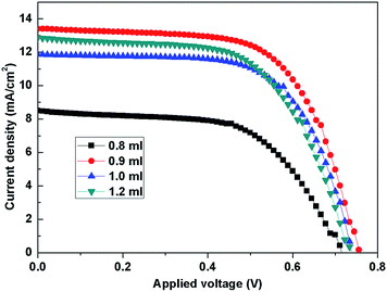
To obtain superior DSSCs with excellent photovoltaic performance, the amount of titanium precursor added for 1D/3D nanorod synthesis was optimized. The etching-time was fixed at 12 h, while the amount of the titanium precursor was set to 0.8, 0.9, 1.0 and 1.2 ml. The influence of the titanium precursor amount toward the photovoltaic performance of the assembled DSSCs was investigated. Fig. 7 presents the typical J–V curves of these cells made from different titanium precursor amounts and the detailed parameters of these cells are summarized in Table 2. It can be found that the cells synthesized with 0.9 ml tetrabutyl titanate exhibit the highest Jsc of 13.47 mA cm−2 and the largest Voc of 0.76 V, which resulted in the highest recorded efficiency of 6.44%.
 |
| | Fig. 7 The J–V characteristics of DSSCs based on the TiO2 network structure films which were synthesized using different amounts of titanium precursor and followed by etching treatment for 12 h. | |
Table 2 Detailed photovoltaic properties of DSSCs based on the TiO2 network structure films synthesized using different amounts of titanium precursor
| Sample |
Voc (V) |
Jsc (mA cm−2) |
Fill factory |
Efficiency |
| 0.8 ml |
0.72 |
8.62 |
57.84 |
3.59 |
| 0.9 ml |
0.76 |
13.47 |
62.90 |
6.44 |
| 1.0 ml |
0.74 |
11.95 |
64.23 |
5.68 |
| 1.2 ml |
0.74 |
12.94 |
59.42 |
5.69 |
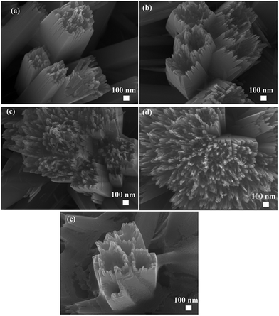
Many methods were developed to improve the photovoltaic properties of DSSCs; among all of these methods, immersing the TiO2 films in titanium tetrachloride (TiCl4) solution was regarded as the most effective way. After this modification, extra TiO2 nanoparticles can be synthesized through TiCl4 hydrolysis on the surface of the prepared TiO2 films, which leads to further enlargement of the TiO2 surface area. Consequently, it improves the amount of dye molecules adsorbed on the photoanode surface. Moreover, several publications reported that TiCl4 post-treatment can also improve the light scattering capacity and prevent the electrons in the photoanode from recombining with the electrolyte.38–40 The above results indicated that the optimum preparation conditions of the TiO2 photoanode were 0.9 ml of titanium precursor followed by 12 h etching treatment. In this work, TiCl4 treatment was conducted on the TiO2 network structure films prepared under optimum conditions for further improvement in cell performance. We fabricated four samples by immersing the TiO2 photoanodes in 0.1 M TiCl4 solution at room temperature for 0, 12, 36 and 48 h, respectively. The resultant TiO2 films were annealed at 450 °C for 30 min. Fig. 8 displays the SEM images of the four samples modified with TiCl4 for various times. It can be observed from Fig. 8a that the 3D nanorods were transformed into nanotube structures after etching treatment and the surface of the nanotubes is smooth. After 12 h TiCl4 treatment, the profile of the nanotubes was attached with a lot of nanoparticles which roughened the surface and the size of the nanoparticles was about 10 nm. Moreover, Fig. 8c reveals that the amount and the size of the nanoparticles increased with the immersion time. When the treatment duration was prolonged to 48 h, the inside and outside surface of the nanotube was filled with a large number of TiO2 nanoparticles. The more detailed morphology of the sample with 48 h TiCl4 post-treatment is shown in Fig. 3s.† It can be seen that the films maintained the 3D nanoflower structure, which was composed of several nanotube petals. Compared with the un-treated sample, the inner diameter of this nanotube decreased, which is ascribed to the increased amount of the TiO2 nanoparticles attached on the inner surface of the nanotubes. Fig. 3sa and b† show the top view and cross-sectional SEM images of the one-dimension nanowire arrays on the bottom layer after 48 h TiCl4 treatment. It can be observed that the tip and the profile of the nanowire arrays were covered with abundant TiO2 nanoparticles. In addition, the high magnification SEM images display that the average diameter of the TiO2 nanoparticles is approximately 20 nm.
 |
| | Fig. 8 The top-view images of the TiO2 network structure immersed in TiCl4 solution for different times. (a) 0 h, (b) 12 h, (c) 36 h and (d) 48 h. | |
Fig. 9 exhibits the J–V curves of the DSSCs assembled from the TiO2 photoanode which was treated with TiCl4 for different times and the corresponding photovoltaic parameters are listed in Table 3. The noteworthy point here is that TiCl4 modification remarkably increased Jsc, which reached a maximum value of 18.30 mA cm−2 for the 48 h treatment sample. The Jsc value increasing with TiCl4 post-treatment time can be explained as follows: as the SEM images (Fig. 8) show, TiCl4 immersion gave rise to the hydrolysis of TiCl4 and generated lots of TiO2 nanoparticles attached on the TiO2 films surface, involving the 1D nanowire arrays on the bottom layer and the 3D nanotubes on the top layer. Moreover, the amount of TiO2 nanoparticles increased with treatment time, which improved the specific surface area of the TiO2 films, leading to the enhancement of dye-loading ability. In addition, it was found that the PCE values of the DSSCs presented a slight decrease when the TiCl4 treatment time increased from 0 to 12 h, then increased as the treatment time was further prolonged to 36 or 48 h. Whereas the OCV and FF always exhibited an obvious decrease with TiCl4 treatment times, it maybe due to the increase of the sheet resistance after TiCl4 treatment. These results suggest that the increase of PCE was derived mostly from the enhancement of the photocurrent density. Moreover, a thin TiO2 layer covered the bare surface of the FTO substrate after TiCl4 treatment, which blocked recombination between electrons in the photoanode and positive charge in the electrolyte. In addition, modification using TiCl4 can also improve the light scattering capacity of the TiO2 films. All these functions of TiCl4 treatment resulted in high energy conversion.
 |
| | Fig. 9 The J–V curves of DSSCs based on TiO2 network structure films immersed in the TiCl4 solution for different times. | |
Table 3 Photovoltaic parameters of DSSCs assembled by 12 h etching TiO2 network structure films immersed in TiCl4 solution for different times
| Sample |
Voc (V) |
Jsc (mA cm−2) |
Fill factory |
Efficiency |
| 0 h |
0.76 |
13.47 |
62.90 |
6.44 |
| 12 h |
0.71 |
14.52 |
59.56 |
6.14 |
| 24 h |
0.71 |
16.96 |
58.30 |
7.02 |
| 48 h |
0.72 |
18.30 |
58.29 |
7.68 |
4. Conclusions
TiO2 films with 1D/3D nanorod network structures have been successfully prepared on a transparent conductive FTO glass substrate via a facile one-step hydrothermal method. In order to further enlarge the surface area, an etching treatment was conducted on the TiO2 network structure films. Comprehensive studies concerning the effects of the etching time on the performance of the TiO2 network structure films were presented. The results showed that the etching treatment using hydrochloric acid did not destroy the crystalline rutile properties of the TiO2 films. In addition, the light-scattering ability and electron-lifetime of the TiO2 films decreased as the etching duration increased. These were attributed to the reduced length of the TiO2 nanostructure, including the petals of the 3D nanostructure in the top layer and the nanowires in the bottom layer. For the 14 h etching sample, the splitting rate of secondary nanowires balanced with the TiO2 dissolution velocity, the amount and the length of the secondary nanowires reached a maximum, which resulted in the largest surface area and best dye-loading ability of the TiO2 network structure films. After optimizing the titanium precursor amount and the TiCl4 post-treatment time, an outstandingly high efficiency of 7.68% was achieved from the TiO2 films with this novel structure, which was synthesized using 0.9 ml tetrabutyl titanate followed by 12 h of etching and 48 h TiCl4 post-treatment.
Acknowledgements
This work is supported in part by the National Natural Science Foundation of China (No. 51372075, 51502084), Research Fund for the Doctoral Program of Higher Education of China (RFDP, No. 20124208110006).
References
- B. O. Regan and M. Grätzel, Nature, 1991, 35, 737–740 CrossRef PubMed.
- M. Grätzel, Acc. Chem. Res., 2009, 42, 1788–1798 CrossRef PubMed.
- C. P. Lee, R. Y. Lin, L. Y. Lin, C. T. Li, T. C. Chu, S. S. Sun, J. T. Lin and K. C. Ho, RSC Adv., 2015, 5, 23810–23825 RSC.
- J. J. Lin, Y. U. Heo, A. Nattestad, M. Shahabuddin, Y. Yamauchi and J. H. Kin, Phys. Chem. Chem. Phys., 2015, 17, 7208–7213 RSC.
- J. J. Lin, A. Nattestad, H. Yu, Y. Bai, L. Z. Wang, S. X. Dou and J. H. Kim, J. Mater. Chem. A, 2014, 2, 8902–8909 CAS.
- X. Yu, H. Wang, Y. Liu, X. Zhou, B. J. Li, L. Xin, Y. Zhou and H. Shen, J. Mater. Chem. A, 2013, 1, 2110–2117 CAS.
- S. M. Wang, W. W. Dong, R. H. Tao, Z. H. Deng, J. Z. Shao, L. H. Hu, J. Zhu and X. D. Fang, J. Power Sources, 2013, 235, 193–201 CrossRef CAS PubMed.
- Z. Q. Sun, J. H. Kim, Y. Zhao, D. Attard and S. X. Dou, Chem. Commun., 2013, 49, 966–968 RSC.
- B. Liu and E. S. Aydil, J. Am. Chem. Soc., 2009, 131, 3985–3990 CrossRef CAS PubMed.
- J. T. Jiu, S. J. Isoda, F. M. Wang and M. Adachi, J. Phys. Chem. B, 2006, 110, 2087–2092 CrossRef CAS PubMed.
- P. L. Kuo, T. S. Jan, C. H. Liao, C. C. Chen and K. M. Lee, J. Power Sources, 2013, 235, 297–302 CrossRef CAS PubMed.
- S. H. Kang, S. H. Choi, M. S. Kang, J. Y. Kim, H. S. Kim, T. Hyeon and Y. E. Sung, Adv. Mater., 2008, 20, 54–58 CrossRef CAS PubMed.
- M. Zhu, L. Chen, H. B. Gong, M. Zi and B. Q. Cao, Ceram. Int., 2014, 40, 2337–2342 CrossRef CAS PubMed.
- H. Yu, J. Pan, Y. Bai, X. Zong, X. Y. Li and L. Z. Wang, Chem.–Eur. J., 2013, 19, 13569–13574 CrossRef CAS PubMed.
- S. S. Mali, H. Kim, C. S. Shim, W. R. Bae, N. L. Tarwal, S. B. Sadale, P. S. Patil, J. H. Kim and C. K. Hong, CrystEngComm, 2013, 15, 5660–5667 RSC.
- Z. Q. Sun, J. H. Kim, Y. Zhao, F. Bijarbooneh, V. Malgras, Y. M. Lee, Y. M. Kang and S. X. Dou, J. Am. Chem. Soc., 2011, 133, 19314–19317 CrossRef CAS PubMed.
- M. Q. Lv, D. J. Zheng, M. D. Ye, L. Sun, J. Xiao, W. X. Guo and C. J. Lin, Nanoscale, 2012, 4, 5872–5879 RSC.
- M. Q. Lv, D. J. Zheng, M. D. Ye, J. Xiao, W. X. Guo, Y. K. Lai, L. Sun, C. J. Lin and J. Zuo, Energy Environ. Sci., 2013, 6, 1615–1622 CAS.
- H. Wang, Y. S. Bai, H. Zhang, Z. H. Zhang, J. H. Li and L. Guo, J. Phys. Chem. C, 2010, 114, 16451–16455 CAS.
- H. Wang, B. Y. Wang, J. C. Yu, Y. X. Hu, C. Xia, J. Zhang and R. Liu, Sci. Rep., 2015, 5, 9305 CrossRef CAS PubMed.
- J. Zhang, S. Q. Li, H. Ding, Q. T. Li, B. Y. Wang, X. N. Wang and H. Wang, J. Power Sources, 2014, 247, 807–812 CrossRef CAS PubMed.
- J. Zhang, Q. T. Li, S. Q. Li, Y. Wang, C. Ye, P. Ruterana and H. Wang, J. Power Sources, 2014, 268, 941–949 CrossRef CAS PubMed.
- A. Kumar, A. R. Madaria and C. W. Zhou, J. Phys. Chem. C, 2010, 114, 7787–7792 CAS.
- H. M. Cheng, J. M. Ma, Z. G. Zhao and L. M. Qi, Chem. Mater., 1995, 7, 663–671 CrossRef CAS.
- L. Liu, J. S. Qian, B. Li, Y. M. Cui, X. F. Zhou, X. F. Guo and W. P. Ding, Chem. Commun., 2010, 46, 2402–2404 RSC.
- N. G. Park, J. V. Lagemaat and A. J. Frank, J. Phys. Chem. B, 2000, 104, 8989–8994 CrossRef CAS.
- S. Powar, Q. Wu, M. Weidelener, A. Nattestad, Z. Hu, A. Mishra, P. Bäuerle, L. Spiccia, Y. B. Cheng and U. Bach, Energy Environ. Sci., 2012, 5, 8896–8900 CAS.
- H. M. Zhang, Y. H. Han, P. Liu, H. Yu, S. Q. Zhang, X. D. Yao and H. J. Zhao, Chem. Commun., 2010, 46, 8395–8397 RSC.
- J. Kim, J. K. Koh, B. Kim, J. H. Kim and E. Y. Kim, Angew. Chem., 2012, 124, 6970–6975 CrossRef PubMed.
- J. B. Na, J. H. Kim, C. Y. Park and E. Y. Kim, RSC Adv., 2014, 4, 44555–44562 RSC.
- S. Hore, C. Vetter, R. Kern, H. Smit and A. Hinsch, Sol. Energy Mater. Sol. Cells, 2006, 90, 1176–1188 CrossRef CAS PubMed.
- H. J. Koo, Y. J. Kim, Y. H. Lee, W. I. Lee, K. Kim and N. G. Park, Adv. Mater., 2008, 20, 195–199 CrossRef CAS PubMed.
- Y. Tachibana, K. Hara, K. Sayama and H. Arakawa, Chem. Mater., 2002, 14, 2527–2535 CrossRef CAS.
- L. Kavan, J. H. Yum and M. Grätzel, ACS Nano, 2011, 5, 165–172 CrossRef CAS PubMed.
- A. Hagfeldt, G. Boschloo, L. C. Sun, L. Kloo and H. Pettersson, Chem. Rev., 2010, 110, 6595–6663 CrossRef CAS PubMed.
- J. Bisquert, A. Zaban, M. Greenshtein and I. Mora-Seró, J. Am. Chem. Soc., 2004, 126, 13550–13559 CrossRef CAS PubMed.
- A. Zaban, M. Greenshtein and J. Bisquert, ChemPhysChem, 2003, 4, 859–864 CrossRef CAS PubMed.
- A. Sedghi and H. N. Miankushki, Jpn. J. Appl. Phys., 2013, 52, 075002 CrossRef.
- J. Liang, G. M. Zhang and W. T. Sun, RSC Adv., 2014, 4, 6746–6751 RSC.
- D. B. Menzies, Q. Dai, L. Bourgeois, R. A. Caruso, Y. B. Cheng, G. P. Simon and L. Spiccia, Nanotechnology, 2007, 18, 125608 CrossRef.
Footnote |
| † Electronic supplementary information (ESI) available. See DOI: 10.1039/c5ra16458c |
|
| This journal is © The Royal Society of Chemistry 2015 |
Click here to see how this site uses Cookies. View our privacy policy here. 


