Jun Gou*,
Jun Wang,
Xing Zheng,
Deen Gu,
He Yu and
Yadong Jiang
State Key Laboratory of Electronic Thin Films and Integrated Devices, University of Electronic Science and Technology of China, No. 4, Section 2, North Jianshe Road, Chengdu 610054, People's Republic of China. E-mail: goujun@uestc.edu.cn; Fax: +86 2883206123; Tel: +86 2883207086
First published on 29th September 2015
Real-time, continuous-wave terahertz (THz) detection and imaging are demonstrated with a 2.52 THz far-infrared CO2 laser and a 320 × 240 vanadium oxide (VOx) micro-bolometer focal plane array. A nanostructured titanium (Ti) thin film absorber is integrated in the micro-bridge structure of the VOx micro-bolometer by a combined process of magnetron sputtering and reactive ion etching (RIE), and its improvement of THz absorption is verified by an optical characteristics test. By eliminating the background signal, non uniformity and noise with proper circuits, the output dynamic range of the readout integrated circuit (ROIC) is 0.4–3.6 V and the fixed pattern noise (FPN) is less than 10 mV. After vacuum packaging, the detector is used for THz detection and achieves a responsivity of 2186 v/w and a NEP of 45.7 pW/Hz1/2. With this detecting system, THz imaging through a wiping cloth and envelope is demonstrated, showing the feasibility of real-time security checking and mail screening.
This paper presents experimental results on real-time detection and imaging of 2.52 THz radiation from far-infrared CO2 laser, using 320 × 240 vanadium oxide (VOx) microbolometer focal plane array with a nanostructured Ti thin film absorber prepared by a combined process of magnetron sputtering and reactive ion etching (RIE). Firstly, nanostructured Ti films are prepared with different thicknesses and the improvement of THz absorption is analyzed by surface morphology test. Then, micro-bridge fabrication is described and optical characteristics is tested. Readout circuit for eliminating background signal, non uniformity and noise is designed, vacuum assembly structure and packaging process are also described. Finally, responsivity and NEP of pixel are evaluated and THz imaging through wiping cloth and envelope is demonstrated.
Etch time (s) | Square resistance (Ω □−1) | Thickness (nm) | |
---|---|---|---|
1 | 450 | 160 | 5 |
2 | 330 | 88.9 | 9 |
3 | 240 | 69.6 | 11.5 |
4 | 180 | 57.1 | 14 |
5 | 120 | 49.9 | 16 |
The measured transmission and reflection curves of Ti thin films thinned by RIE with different thicknesses are shown in Fig. 1(a) and (b), respectively. Here, it is not accurate to calculate the absorption of Ti thin film at the same frequency for different light paths for transmission and reflection tests. But we can do qualitative comparison of reflection and transmission to discuss absorption performance of Ti films. It can be seen from Fig. 1(a) that THz transmission of Ti thin film decreases with the increase of film thickness. Fig. 1(b) shows that THz reflection of Ti thin film decreases with the increased thickness when the thickness is larger than 9 nm. But the reflection of Ti thin film with a thickness of 9 nm is lower than that of Ti thin film with a thicknesses of 5 nm. It seems that 9 nm Ti film has a lower transmission and reflection compared to 5 nm Ti film, which implies its higher absorption of terahertz radiation due to the relationship between transmission (T), reflection (R) and absorption (A): T + R + A = 1. The optimized thickness is similar to that of NiCr thin film prepared by similar method in our earlier research21 for Ti thin film has a similar value of electrical conductivity with NiCr thin film.
![]() | ||
Fig. 1 The measured (a) transmission and (b) reflection curves of Ti thin films thinned by RIE with different thicknesses. |
In order to study surface morphology and structure of Ti thin film, Fig. 2 shows the AFM images of 20 nm Ti thin film directly deposited by magnetron sputtering and 9 nm Ti thin film prepared by a combination of magnetron sputtering and RIE. It is clear that the directly deposited Ti thin film has a very smooth surface while the RIE treated Ti thin film has a roughened surface. Nanostructured Ti thin film is obtained by RIE with nano-scale surface structures and a increased specific surface area. It is known that the absorption of a metal film consists of two components:19,22 the intrinsic absorption of an ideally smooth surface and the contribution due to nano-scale surface structures, which contributed to the enhancement of THz absorption. So the combined process of magnetron sputtering and RIE can prepare Ti thin film with a small thickness by precise control of RIE process, at the same time it is an effective method to obtain nanostructured Ti thin film for further improvement of THz absorption.
![]() | ||
Fig. 2 SEM images of (a) 20 nm Ti thin film directly deposited by magnetron sputtering and (b) 9 nm Ti thin film prepared by a combination of magnetron sputtering and RIE. |
The reflection layer was made of NiCr thin film with a thickness of 250 nm which was also patterned as the bottom electrode by wet etching with a solution of ammonium cerium nitrate ((NH4)2Ce(NO3)6) and nitrate (HNO3). To prepare suspended micro bridge, photo sensitive polyimide pattern with a thickness of 2.5 μm was prepared as sacrificial layer on the reflection layer, which could be removed by oxygen (O2) plasma. The diaphragm was fabricated on the sacrificial layer. 250 nm Si3N4 thin film acting as the support layer was deposited by plasma enhanced chemical vapor deposition (PECVD) from SiH4/NH3 at a temperature of 350 °C, and patterned by RIE using a gas mixture of CHF3 and O2. VOx thin film was prepared on the support layer as the thermal sensitive layer with a film thickness of 50 nm and a temperature coefficient of resistance (TCR) of ∼ −2.3%/K by magnetron sputtering with a sputter power of 300 W, a partial pressure of oxygen of 0.5%, and an annealing temperature of 350 °C at vacuum environment. A Si3N4 passivation film was deposited on VOx layer by PECVD with a thickness of 100 nm, on which Ti thin film acting as THz wave absorption layer was fabricated. Here, 20 nm Ti thin film directly deposited by magnetron sputtering and 9 nm Ti thin film thinned by RIE were prepared and patterned, respectively. 320 × 240 THz focal-plane array without Ti thin film absorber was also fabricated. After etching the top membrane by RIE, the photo sensitive polyimide (sacrificial layer) was released completely by O2 plasma at 280 °C to form suspended micro-bridge structure in each pixel. SEM image of single pixel and three-dimensional microscopic image of THz focal-plane array are shown in Fig. 4.
![]() | ||
Fig. 4 (a) SEM images of single pixel and (b) three-dimensional microscopic image of THz focal-plane array. |
The reflections of the fabricated 320 × 240 THz focal-plane arrays measured by the FTIR system are shown in Fig. 5. The reflections of THz focal-plane arrays with Ti absorption films are reduced compared to that of THz focal-plane array without Ti thin film absorber. 9 nm RIE treated Ti thin film shows greater contribution on the reduction of reflection. Since the transmission at the reflection layer in each pixel can be negligible and Ti absorption film is patterned on the top of the reflection layer, so the transmissions can be considered as a constant value for the three kinds of THz focal-plane arrays. Based on this assumption, it can be concluded that lower reflection of THz focal-plane array is caused by its higher THz absorption. It is clear that 9 nm RIE treated Ti thin film provides higher absorption of THz radiation. This provides an effective way which is easy to accomplish and compatible with the manufacturing process of THz focal-plane array to fabricate THz absorption layer and improve detection performance.
![]() | ||
Fig. 5 Measured reflections of 320 × 240 THz focal-plane arrays without Ti absorption film and with Ti absorption film. |
Fig. 6 shows an architecture of ROIC for THz focal-plane array, which is composed of unit circuit (input stage), column signal processing circuit, high speed buffer output stage, line/column selection signal generating circuit and clock control signal generating circuit.
When a constant voltage is applied to the pixel, a large current value is generated (called the background current signal) due to high resistance value even without target radiation. If this current is amplified by integral, the integrator output is very easy to reach saturation and unable to characterize the amount of radiation. Due to the existence of non uniformity, dynamic range of output will be lost and the imaging quality will be seriously affected. So the elimination of high background signal and non uniformity is particularly important.
The elimination of high background signal is achieved by chosing the useful signal current for integral amplification, which means the bias current change caused by the change of the resistance when the change of THz radiation is detected by the pixel. The schematic diagram of circuit for background signal elimination is shown in Fig. 7(a), in which I3, rather than I2, is integral amplified. The non uniformity is eliminated by correlated double sampling shown in Fig. 7(b). Non uniformity caused by the offset of operational amplifier is eliminated using this circuit.
![]() | ||
Fig. 7 Schematic diagrams of (a) circuit for background signal elimination and (b) correlated double sampling circuit. |
As shown in Fig. 7, the resistance of the pixel (Rs) has a very small change since a small change of the amount of radiation is detected. So I3 is a very weak signal which is pA magnitude. In addition to amplifying useful weak signal, the ROIC should also suppress or reduce noise for higher signal to noise ratio (SNR) of output signal. Weak signal can be read out by appropriately increasing integral time and reducing integral capacitance. High frequency noise can be reduced by the frequency response characteristic of low-pass filter in the integrator. Low frequency noise can be eliminated by the method of correlated double sampling. The coupling noise of the substrate is eliminated by trap isolation for the integral capacitance and the sample-hold capacitance. The output dynamic range of the ROIC achieved 0.4–3.6 V and the fixed pattern noise (FPN) noise was less than 10 mV.
In order to improve the response, the detector was vacuum packaged to reduce the thermal conductivity, heat radiation and noise. Vacuum packaging structure for THz detector is mainly composed of shell (socket), thermoelectric cooler (TEC), ceramic substrate, detector chip, getter, thermal baffle, cap and optical window. All components are assembled into a complete vacuum packaged system by high precision assembly, as shown in Fig. 8.
TEC was used to provide a stable operating point to the chip. Getter was integrated to adsorb the gas generated inside the assembly for a stable high vacuum. Due to relatively high temperature for the activation of getter, a thermal baffle was designed to keep thermal radiation of getter from detector chip and TEC and prevent damages during the activation process. TEC was welded to shell by metal welding for heat radiation and reliable connection. Optical window was welded to the cap by eutectic furnace welding and the cap is then welded to the shell with all other components fitted inside by laser welding to form a packaged assembly. After exhaust and pinch sealing, vacuum in the shell was higher than 10−5 Pa and leakage rate of the packaged assembly was measured to be lower than 2 × 10⁻¹³ Pa m3 s−1.
The tests were carried out with an environment temperature of 296 K and a relative humidity of 50%. The dewar with THz detector inside was connected to pump which kept the vacuum level inside the dewar under 1 × 10⁻³ Pa. A constant current offset of 1 μA was applied to the sensing element by a low noise current source (KEITHLEY 4200). When doing noise voltage test, small signal noise voltage was measured by a phase-locked amplifier (SR850) without target radiation. For response voltage test, a high power CO2 laser (FIRL 100) which generated 2.52 THz radiation was used as THz radiation source. Because of the poor uniformity of the beam with a beam width of 10 mm and a divergence angle of 13 mrad, a throughhole with a diameter of 5 mm was set in the center of the beam in the light path. The radiation power through the throughhole and an optical window was measured to be 5.7 mW at the detector position by a THz power meter (Vector H410). The THz radiation power on single sensing element (35 μm × 35 μm) was calculated to be 0.3558 μW under the assumption that the laser power was equal in the whole throughhole area which was much smaller than the beam. By setting the reference frequency and chopping frequency to 20 Hz, the noise voltage and peak value of response voltage of the sensing element were tested to be 100 nV/Hz1/2 and 1.1 mV, respectively. So the responsivity was calculated to be 2186 v/w and the NEP was measured to be 45.7 pW/Hz1/2.
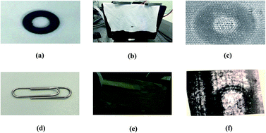
The experimental arrangement for THz imaging is shown in Fig. 9. THz beam generated by CO2 laser was collected and focused with two off-axis paraboloid mirrors onto the THz focal plane array through the silicon optical window on the vacuum packaged assembly. As shown in Fig. 10, images of a metallic circular washer covered by a piece of wiping cloth and a paper clip hidden in an envelope were obtained by the detector. Fig. 10(c) shows a THz image of the metallic circular washer covered by a piece of wiping cloth (made from 100% polyester fiber), demonstrating the feasibility of security checking. Fig. 10(f) shows a THz image of the paper clip hidden in an envelope (made from kraft paper), demonstrating the feasibility of mail screening.
In conclusion, our imaging system demonstrates the use of a 320 × 240 THz focal plane array for real-time, continuous-wave 2.52 THz imaging with a far infrared CO2 laser. Improvements in spatial resolution can be made by designing pixel structure and optics including using different radiation absorbing materials and fabricating appropriate antireflective structures on the optical window.
This journal is © The Royal Society of Chemistry 2015 |