
Tailoring the electrical properties of multilayer MoS2 transistors using ultraviolet light irradiation†
Arun Kumar Singh*ab,
Shaista Andleebb,
Jai Singhc and
Jonghwa Eomb
aDepartment of Physics, Motilal Nehru National Institute of Technology, Allahabad-211004, India. E-mail: arunsigh.itbhu@gmail.com
bDepartment of Physics and Graphene Research Institute, Sejong University, Seoul 143-747, Korea
cDepartment of Nano Science and Technology, Institute of Nano and Advanced Materials Engineering, Sejong University, Seoul 143-747, Korea
First published on 3rd September 2015
Abstract
Two dimensional layered semiconductor transition-metal dichalcogenides such as molybdenum disulfide (MoS2) have attracted tremendous interest as a new class of electronic material and generated considerable attention as a promising channel material for field-effect transistors (FETs). Modulating the electronic properties of MoS2 is essential in order to obtain the best performance of its electronic and optoelectronic devices as well as enabling fabrication of various complex devices. In this paper we report a very straightforward and simple technique to tailor the performance of multilayer (ML) MoS2 FETs by exposure to nitrogen (N2) gas under deep-ultraviolet (DUV) light. Threshold voltages of ML MoS2 FETs shifted towards a negative gate voltage after exposure to N2 gas in the presence of DUV light. We also observed that drain-to-source current, carrier density and charge-carrier mobility of ML MoS2 are significantly improved after exposure to N2 gas under DUV light irradiation.
1. Introduction
In recent years, two dimensional (2D) layered transition metal dichalcogenides (TMDCs) such as molybdenum disulfide (MoS2) have attracted tremendous research attention due to their exciting electrical and optical properties.1–4 MoS2 exhibits many other excellent properties such as superior mechanical flexibility, impressive thermal stability, absence of dangling bonds and compatibility with silicon CMOS processes, as similar to its well-known cousin, graphene.5,6 However, it is totally distinct from graphene in context of band-gap, graphene has linear dispersion characteristic and absence of band-gap in the electronic band structure.7,8 The absence of energy gap in graphene limits its practical applications in logic circuits applications. MoS2 is a n-type semiconductor with thickness-dependent band-gap of 1.2 to 1.8 eV (single-layer MoS2 has a direct band-gap of 1.8 eV and bulk MoS2 has an indirect band-gap of 1.2 eV).9,10Due to presence of band-gap, MoS2 based fascinating electronic devices including field-effect transistors (FETs), ultrasensitive photodetectors, chemical and bio sensors, nonvolatile memory devices, integrated circuits and supercapacitors have already been demonstrated.11–17 Among these devices, the FET is the most important and is a basic building block of any logic circuit/device. Nowadays, majority of the efforts have been focused to improve the performance of MoS2 FETs by integration of MoS2 devices in the back or dual-gated geometry, using different metal contacts (source and drain electrodes), scaling down the device dimensions, doping of MoS2 with metal nanoparticles, or with self-assembled monolayers or molecules.18–23 Doping is the most effective and easy technique to modify the electrical characteristics of any semiconducting material. The controlled doping in MoS2 is not only essential for tuning the charge density and electronic properties but also enabling fabrication of various complex devices. However, tuning the electrical properties of ML MoS2 has not yet explored. Few previous reports suggested that ML MoS2 may be better than single-layer MoS2 in FET applications because it has a larger density of states.24,25 The larger density of state helps to create a larger channel carrier density, which boosts the current drive of FETs. The large drive current has better noise immunity in air. In addition, ML MoS2 is more suitable and easy for practical fabrication process.
In this paper, we report the enhancement as well as tailoring the electrical properties of multilayer MoS2 by N2 gas under deep-ultraviolet (DUV) light irradiation. ML MoS2 were obtained by micromechanical exfoliation and identified by optical microscope and Raman spectroscopy. The fabricated FET of ML MoS2 flakes are exposed to N2 gas in the presence of DUV light for different periods. The electrical transport measurements are used to investigate the changes in electrical properties of ML MoS2 after exposing to N2 gas in the presence of DUV light for different periods of time. The threshold voltages are shifted towards the negative gate voltage after exposure to N2 gas in the presence of DUV light, which reveals the n-doping of ML MoS2 FETs. The exposure of DUV light in the presence of N2 gas remarkably improves the drain-to-source current, carrier density and charge-carrier mobility of ML MoS2.
2. Experimental section
2.1. Sample preparation
ML MoS2 flakes were obtained by micromechanical exfoliation of naturally occurring crystals of molybdenite (SPI supplies, USA) using Scotch tape and transfer on a 300 nm SiO2 substrate with underlying highly p-doped silicon. The ML MoS2 films were characterized by optical contrast and Raman spectroscopy. Atomic force microscopy (AFM) was used to measure the thickness of the samples. Raman spectra were collected at room temperature with a Renishaw microspectrometer having a laser wavelength of 514 nm.2.2. Device fabrication and measurements
The big patterned electrodes Cr/Au thickness of (6/30 nm) for ML MoS2 films were made by optical lithography. Source and drain electrodes were patterned employing e-beam lithography and evaporation of Cr/Au (6/80 nm). The channel length and width are ∼1.5 μm and ∼3 μm. The devices were annealed in a tube furnace at a temperature of 200 °C, in a flow of 100-sccm Ar and 10-sccm H2 for 4 hours to remove the residue and minimize the contact resistance of the devices. The fabricated FETs of ML MoS2 were electrically characterized using a Keithley 2400 source meter and Keithley 6485 picometer at room temperature in a vacuum.2.3. Ultraviolet-light irradiation and characterizations
ML MoS2 films were exposed to N2 gas flow in the presence of DUV light (λ = 220 nm, average intensity of 10 mW cm−2) for different periods. After each exposure to DUV and N2 gas, devices were characterized by Raman spectroscopy and measurements of electrical transport. The sample chamber was vacuum pumped for 30 minutes before each electrical measurement and during each measurement. All electrical measurements were conducted in a vacuum at room temperature.3. Results and discussion
Fig. 1a displays optical micrograph of ML MoS2 layers. An optical microscope was used to identify the ML MoS2, which were further characterized by Raman spectroscopy. On the basis of contrast, we can easily identified ML MoS2 flakes. It is well know that different layer have different contrast on Si/SiO2 substrate and yield of ML MoS2 flakes is much higher than single or bi-layer MoS2 flakes. Thickness of ML MoS2 flakes was measured by AFM and thickness of the ML MoS2 is about 5.5 nm, which indicates 8 layers of MoS2 as given Fig. S1 in ESI.† Fig. S2 in ESI† displays typical Raman spectra of ML MoS2 layer on Si/SiO2 substrate. Raman spectra were collected at room temperature with a Renishaw micro spectrometer having a laser wavelength of argon ion laser (λ = 514 nm). E12g and A1g are located at 383.5 and 407.8 cm−1, respectively for ML MoS2, it is consistent with previously reported results.26–28 The frequency difference between two peaks (E12g and A1g) is also revealed that MoS2 flakes are multilayer, frequency difference is about 24.3 cm−1.29 Fig. 1b shows the scanning electron microscopy (SEM) image of fabricated device. First, the big patterned electrodes (Cr/Au ratio of 5/30 nm) around selected ML MoS2 were made employing photolithography on Si/SiO2 substrate. The source and drain electrodes of transistors were made using e-beam lithography, consisting of 5 nm of Cr covered by 80 nm of Au. The channel length and width are ∼1.5 μm and ∼3 μm. We have made several multilayer devices of nearly same thickness and tried to maintain same channel length of the all devices. Fabricated devices were annealed at 200 °C for four hours in a flow of 100 standard cubic centimeters per minute (SCCM) Ar and 10 sccm H2 to remove the residue and contamination, before any electrical characterizations. | ||
| Fig. 1 (a) Optical image of mechanically exfoliated ML MoS2, (b) the SEM image of fabricated ML MoS2 FET device. | ||
The basic electronic properties of MoS2 FETs were first investigated using standard back-gate devices on Si/SiO2 substrate. Fig. 2 shows electrical characterization of our pristine ML MoS2 transistor and all electrical characterizations of our devices are performed at room temperature in a vacuum chamber. The fabricated FETs of ML MoS2 were electrically characterized using a Keithley 2400 source meter and Keithley 6485 picometer. The drain current IDS versus drain–source voltage VDS at different gate voltages (ranging from −6 to +6 V in steps of 2 V) are shown in Fig. 2a. The linear (IDS–VDS) characteristic of our devices shows good ohmic contact with source and drain electrodes. The IDS as a function of the applied back-gate voltage Vg at a fixed drain–source voltage, VDS = 10 mV is depicted in Fig. 2b, which clearly revealed the n-type characteristics.
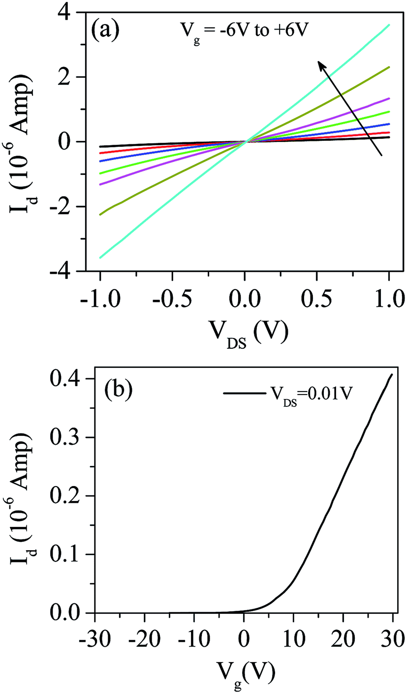 | ||
| Fig. 2 (a) ID–VDS output characteristics at various gate voltages Vbg (ranging from −6 to +6 V with steps of 2 V) for ML MoS2 transistor. (b) The ID–Vbg transfer characteristics of ML MoS2 transistor at VDS = 0.01 V. | ||
After characterizations of our pristine devices, ML MoS2 films were exposed to N2 gas flow in the presence of DUV light (λ = 220 nm, average intensity of 10 mW cm−2) for different periods (5, 10, 20, and 30 min). The schematic illustration of exposure of device under DUV light is shown in Fig. 3a. The effect of exposure of N2 gas in the presence of DUV light irradiation for different period of time is investigated by electrical charge transport measurements and Raman spectroscopy. The sample chamber was vacuum pumped for 30 minutes before each electrical measurement and vacuum pump was also continuously running during each measurement. Fig. 3b shows IDS as a function of Vg before and after N2 exposure under constant DUV light treatment for different periods. The shifting of the threshold voltage towards a negative gate voltage with N2 gas in the presence of DUV light for different periods are shown in Fig. 3b. The shifting of threshold voltage towards a negative gate voltage revealed n-doping in ML MoS2. We have measured the performance of several multilayer devices and observed that effect of DUV light with N2 gas on performance of transistors are nearly same. Of course performance of MoS2 transistor depends on numbers of layers. However, in this manuscript we have focused on the performance of multilayer MoS2 transistor and performance of multilayer devices did not significantly changed with 5 layers to 10–12 layers. The electrical performance of one more ML MoS2 device is shown in Fig. S3 of ESI.†
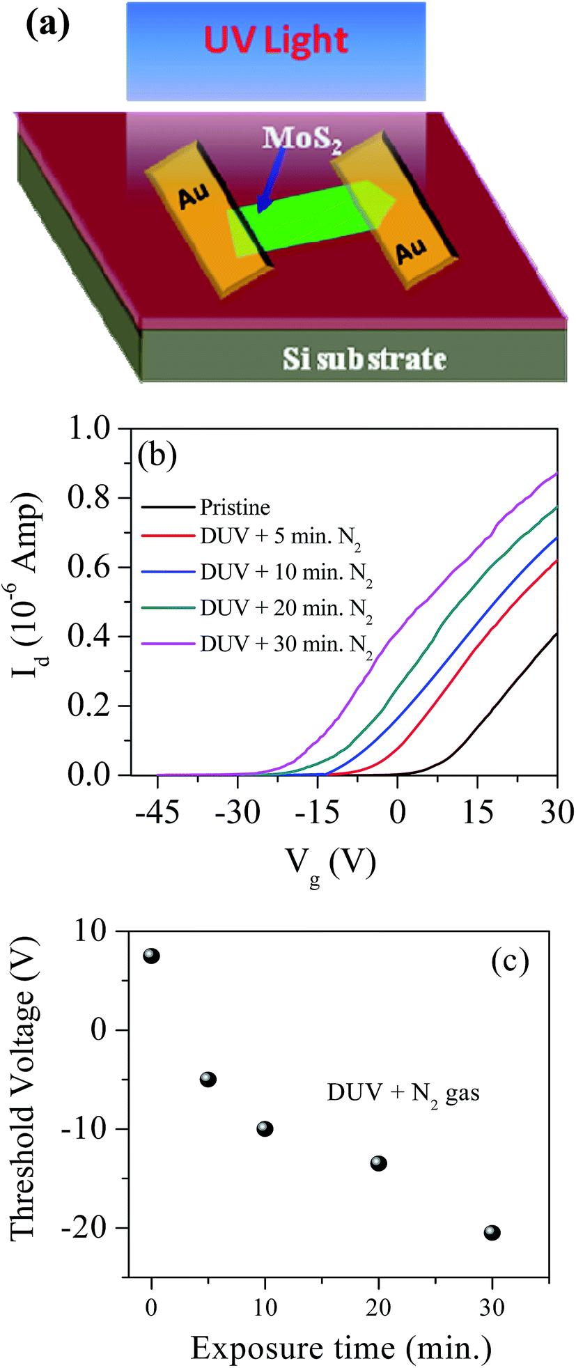 | ||
| Fig. 3 (a) Schematic diagram of exposure of device under DUV light, (b) the ID–Vbg characteristics with different exposure time of N2 gas under DUV light for ML MoS2 transistors. (c) The threshold voltage as a function of the time of exposure of N2 gas in the presence of DUV light for ML MoS2 transistors. | ||
The shifting of threshold voltage toward negative gate voltage (n-doping) of ML MoS2 by exposure of N2 gas under irradiation of DUV light can be understood in terms of the removal of oxygen or an oxygen-derived group from MoS2 nanosheets. The energy dispersive X-ray spectroscopy was used for confirmation of removal of oxygen after exposure of N2 gas under DUV light irradiation. The X-rays were scanned on the area of 100 × 100 nm2 on the different locations of ML MoS2 nanosheets. Table 1 represents the results of the analysis of energy dispersive X-ray spectroscopy of pristine and after 30 minutes N2 gas exposure under DUV light irradiation for ML MoS2 FET. The significant amount of oxygen reduced after 30 minutes exposure of N2 gas under DUV light irradiation as revealed by the result of energy dispersive X-ray spectroscopy.
| Samples | Element | Pristine | After DUV + N2 |
|---|---|---|---|
| ML MoS2 | O | 23.46% ± 0.3% | 22.93% ± 0.2% |
Fig. 3c shows the shifting of the threshold voltage as a function of time of exposure of N2 gas in the presence of DUV irradiation for ML MoS2. The threshold voltage of the device is obtained by extrapolating the linear portion of the curve of IDS versus Vg to zero IDS, the intercept on the Vg axis is the threshold voltage. The threshold voltage of pristine ML MoS2 is found to be 7.5 V, which is shifted to −20.5 V after 30 minutes exposure of N2 gas under DUV light irradiation. ML MoS2 was also characterized by Raman spectroscopy after 30 minutes DUV light irradiation in N2 gas atmosphere. The A1g peak position shifted toward a lower wave number, which also revealed n-doping in ML MoS2 (Fig. S4 ESI†). The shifting of the peaks toward lower wave number position attributed n-doping in ML MoS2. It has already been reported for other systems.13,21
Fig. 4a shows the carrier density of ML MoS2 as a function of exposure time to N2 and in the presence of DUV light. The charge-carrier densities (n) of the devices were estimated using the relation  where VT is the threshold voltage of the device, Vg = 30 V and e is the electronic charge. The carrier densities of ML MoS2 remarkably increase with exposure of N2 gas under irradiation of DUV light for different period of time. We have plotted IDS with function of exposure time to N2 gas in the presence of DUV light at Vg = +4 V and VDS = 0.5 V. The drain current (IDS) drastically increased with exposure time to N2 gas in the presence of DUV light. The considerable improvement in IDS current is due to the removal of oxygen absorbates from MoS2 nanosheets and increase in electron concentrations in ML MoS2 nanosheets. It is well know that oxygen absorbates trap the electrons and decrease the electron density in 2D nanomaterials.30,31 The removal of oxygen is also confirmed by EDX data. In the presence of DUV light, oxygen molecules may be dissociated and removed from flow of N2 gas. However, the exact mechanism is not clear at present. Another possibility is a shifting of Fermi level of MoS2 at the metal–semiconductor interface or lowering of the barrier at interface and increase the drain current. N2 gas alone does not affect the electrical properties of MoS2 nanosheets.30,32 However, N2 gas in the presence of DUV light remarkably affected the electrical properties of MoS2 nanosheets, as reflected in our case.
 | ||
| Fig. 4 (a) The carrier density and drain current ID as a function of the time of exposure of N2 gas in the presence of DUV light for ML MoS2 transistors. (b) The mobility as a function of the time of exposure of N2 gas in the presence of DUV light for ML MoS2 transistors. | ||
Fig. 4b shows the mobility of ML MoS2 as a function of the time of exposure to N2 gas under DUV light illumination. The field effect mobility of the samples was obtained using the relation  where W is the channel width, L is the channel length,
  is the slope of IDS–Vg of the device, VDS = 0.01 V and Cg is the gate capacitance of ∼115 aF μm−2 for our Si/SiO2 substrate. The value of
  is obtained by fitting the linear regime of the transfer characteristic curves of ML MoS2 FETs. The field effect mobility of our pristine ML MoS2 is comparable to previously reported values. The field effect mobility of ML MoS2 is significantly enhanced with exposure of N2 gas under illumination of DUV light.
4. Conclusion
In conclusion, we have presented a very simple and easy technique to enhance the performance of multilayer (ML) MoS2 FETs by exposure of N2 gas under deep-ultraviolet (DUV) light illumination. Electrical transport measurement confirmed that the ML MoS2 FETs showed enhancements in charge carrier mobility, carrier density, and drain current after exposure of N2 gas under DUV light irradiation. Threshold voltages of ML MoS2 FETs shifted towards a negative gate voltage after exposure of N2 gas in the presence of DUV light which revealed n doping effect. We believe that this work provides important scientific insights for improving the electrical properties of emerging layered two-dimensional materials.Acknowledgements
This research was supported by Nano-Material Technology Development Program (2012M3A7B4049888) through the National Research Foundation of Korea (NRF) funded by the Ministry of Science, ICT and Future Planning. This research was also supported by Priority Research Center Program (2010-0020207) and the Basic Science Research Program (2013R1A1A2061396) through NRF funded by the Ministry of Education. Dr A. K. Singh also acknowledges to Department of Science and Technology (DST), India for support.References
- B. Radisavljevic, A. Radenovic, J. Brivio, V. Giacometti and A. Kis, Nat. Nanotechnol., 2011, 6, 147–150 CrossRef CAS PubMed.
- Q. H. Wang, K. Kalantar-zadeh, A. Kis, J. N. Coleman and M. S. Strano, Nat. Nanotechnol., 2012, 7, 699–712 CrossRef CAS PubMed.
- W. Choi, M. Y. Cho, A. Konar, J. H. Lee, G. Cha, S. C. Hong, S. Kim, J. Kim, D. Jena, J. Joo and S. Kim, Adv. Mater., 2012, 24, 5832–5836 CrossRef CAS PubMed.
- D. Jariwala, V. K. Sangwan, D. J. Late, J. E. Johns, V. P. Dravid, T. J. Marks, L. J. Lauhon and M. C. Hersam, Appl. Phys. Lett., 2013, 102, 173107 CrossRef PubMed.
- H. Y. Chang, S. Yang, J. Lee, L. Tao, W. S. Hwang, D. Jena, N. Lu and D. Akinwande, ACS Nano, 2013, 7, 5446–5452 CrossRef CAS PubMed.
- B. Simone, B. Jacopo and K. Andras, ACS Nano, 2011, 5, 9703–9709 CrossRef PubMed.
- A. K. Geim and K. S. Novoselov, Nat. Mater., 2007, 6, 183–191 CrossRef CAS PubMed.
- A. K. Singh, M. Ahmad, V. K. Singh, K. Shin, Y. Seo and J. Eom, ACS Appl. Mater. Interfaces, 2013, 5, 5276–5281 CAS.
- K. F. Mak, C. Lee, J. Hone, J. Shan and T. F. Heinz, Phys. Rev. Lett., 2010, 105, 136805 CrossRef.
- D. Jariwala, V. K. Sangwan, L. J. Lauhon, T. J. Marks and M. C. Hersam, ACS Nano, 2014, 8, 1102–1120 CrossRef CAS PubMed.
- D. Krasnozhon, D. Lembke, C. Nyffeler, Y. Leblebici and A. Kis, Nano Lett., 2014, 14, 5905–5911 CrossRef CAS PubMed.
- J. Lin, H. Li, H. Zhang and W. Chen, Appl. Phys. Lett., 2013, 102, 203109 CrossRef PubMed.
- D. J. Late, Y. K. Huang, B. Liu, J. Acharya, S. N. Shirodkar, J. Luo, A. Yan, D. Charles, U. V. Waghmare, V. P. Dravid and C. N. R. Rao, ACS Nano, 2013, 7, 4879–4891 CrossRef CAS PubMed.
- D. Sarkar, W. Liu, X. Xie, A. C. Anselmo, S. Mitragotri and K. Banerjee, ACS Nano, 2014, 8, 3992–4003 CrossRef CAS PubMed.
- M. S. Choi, G. Lee, Y. Yu, D. Lee, S. H. Lee, P. Kim, J. Hone and W. J. Yoo, Nat. Commun., 2014, 4, 1624 CrossRef PubMed.
- R. Branimir, B. W. Michael and K. Andras, ACS Nano, 2011, 5, 9934–9938 CrossRef PubMed.
- L. Cao, S. Yang, W. Gao, Z. Liu, Y. Gong, L. Ma, G. Shi, S. Lei, Y. Zhang, S. Zhang, R. Vajtai and P. M. Ajayan, Small, 2013, 9, 2905–2910 CrossRef CAS PubMed.
- H. Liu, A. T. Neal and P. D. Ye, ACS Nano, 2012, 6, 8563–8569 CrossRef CAS PubMed.
- H. Liu, K. Xu, X. J. Zhang and P. D. Ye, Appl. Phys. Lett., 2012, 100, 152115 CrossRef PubMed.
- H. Fang, M. Tosun, G. Seol, T. C. Chang, K. Takei, J. Guo and A. Javey, Nano Lett., 2014, 13, 1991–1995 CrossRef PubMed.
- T. S. Sreeprasad, P. Nguyen, N. Kim and V. Berry, Nano Lett., 2013, 13, 4434–4441 CrossRef CAS PubMed.
- Y. Shi, J. K. Huang, L. Jin, Y. Hsu, S. F. Yu, L. J. Li and H. Y. Yang, Sci. Rep., 2013, 3, 1839 Search PubMed.
- D. Kiriya, M. Tosun, P. Zhao, J. S. Kang and A. Javey, J. Am. Chem. Soc., 2014, 136, 7853–7856 CrossRef CAS PubMed.
- H. J. Kwon, J. Jang, K. Sunkook, S. Vivek and C. P. Grigoropoulos, Appl. Phys. Lett., 2014, 105, 152105 CrossRef PubMed.
- S. Kim, A. Konar, W. S. Hwang, J. H. Lee, J. Lee, J. Yang, C. Jung, H. Kim, J. B. Yoo, J. Y. Choi, Y. W. Jin, S. Y. Lee, D. Jena, W. Choi and K. Kim, Nat. Commun., 2012, 3, 1011 CrossRef PubMed.
- H. Li, Q. Zhang, C. C. R. Yap, B. K. Tay, T. H. T. Edwin, A. Olivier and D. Baillargeat, Adv. Funct. Mater., 2012, 22, 1385–1390 CrossRef CAS PubMed.
- H. Li, Z. Yin, Q. He, H. Li, X. Huang, G. Lu, D. W. H. Fam, A. I. Y. Tok, Q. Zhang and H. Zhang, Small, 2012, 8, 63–67 CrossRef CAS PubMed.
- H. Zeng, B. Zhu, K. Liu, J. Fan, X. Cui and Q. M. Zhang, Phys. Rev. B: Condens. Matter Mater. Phys., 2012, 86, 241301 CrossRef.
- C. Lee, H. Yan, L. E. Brus, T. F. Heinz, J. Hone and S. Ryu, ACS Nano, 2010, 4, 2695–2700 CrossRef CAS PubMed.
- W. Park, J. Park, J. Jang, H. Lee, H. Jeong, K. Cho, S. Hong and T. Lee, Nanotechnology, 2013, 24, 095202 CrossRef PubMed.
- Z. Luo, N. J. Pinto, Y. Davilla and A. T. C. Johnson, Appl. Phys. Lett., 2012, 101, 253108 CrossRef PubMed.
- Y. C. Cheng, T. P. Kaloni, Z. Y. Zhu and U. Schwingenschlog, Appl. Phys. Lett., 2012, 101, 073110 CrossRef PubMed.
Footnote |
| † Electronic supplementary information (ESI) available. See DOI: 10.1039/c5ra14509k |
| This journal is © The Royal Society of Chemistry 2015 |