DOI:
10.1039/C5RA14282B
(Paper)
RSC Adv., 2015,
5, 84865-84871
Optical performance improvement of semi-transparent metal film electrodes with biomimetic subwavelength gratings for high-performance optoelectronic device applications†
Received
20th July 2015
, Accepted 29th September 2015
First published on 29th September 2015
Abstract
We fabricated semi-transparent metal electrodes with biomimetic artificial antireflective subwavelength grating (SWG) structures at the surface of an ultraviolet (UV) curable polymer, i.e., Norland Optical Adhesive (NOA) 63, film on polyethylene terephthalate (PET) substrates for semi-transparent optoelectronic applications. The SWG patterns on the NOA63 film/PET were transferred from the silicon master molds with the conical SWG arrays by soft lithography. As a metal electrode, a silver (Ag) layer was deposited on the surface of the NOA63 SWG/PET substrates for different layer thicknesses. Compared with the Ag-coated flat bare PET (i.e., Ag/PET), the Ag/NOA63 SWG/PET showed a superior optical performance over a wide wavelength range of 400–1800 nm. At the Ag layer thickness of 17 nm, the Ag/NOA63 SWG/PET had lower average reflectance (Ravg) and higher average transmittance (Tavg) values of ∼25.1% and ∼33.9% than those (i.e., Ravg ∼ 55.2% and Tavg ∼ 26.4%) of the Ag/PET, respectively, indicating the maximum figure of merit value of 10.23 × 10⁻⁶ ohm−1 (i.e., transmittance of 0.458 at a wavelength of 550 nm and sheet resistance of 39.71 ohm sq.−1). Furthermore, the surface plasmon resonance phenomina (i.e., strong electric and magnetic fields) were observed around the surface of the Ag layer on NOA63 SWGs. Also, it exhibited less angle-dependent optical characteristics at light incident angles of 20–70° under non-polarized light. For optical behaviors, theoretical analyses were also performed by a rigorous coupled-wave analysis method, which gives a similar tendency with the experimentally measured data.
Introduction
Transparent electrodes, which transmit light and transport electrical carriers simultaneously, have been widely utilized in various optoelectronic devices such as photovoltaics (PVs), light emitting diodes (LEDs), displays, touch panels, and transistors.1–4 Over the few past years, transparent conducting oxides (TCOs) including SnO2:F (FTO) and In2O3:Sn (ITO) have been commercially employed in devices due to their good optical and electrical properties (i.e., transmissions > 80% and resistivities < 10−3 ohm cm). In particular, the ITO is the best TCO layer available today in high-performance applications.5,6 However, there has been an increasing demand in the development of transparent electrodes for an alternative of the ITO due to the increasing cost of indium (In) and the additional thermal process. Moreover, its high thickness disrupts a flexible device approach. Many studies are reported on the various transparent electrodes such as conducting polymers,7 metal nanowire meshes,8 carbon-based materials (i.e., carbon nanotubes, graphenes, etc.),9,10 and oxide/metal/oxide hybrid electrodes (i.e., ITO/silver (Ag)/ITO),11 which have been mostly developed for semi-transparent organic device applications including organic PVs, LEDs, and transistors, which offer an extensive range of applications such as power-creation windows for buildings and automobiles, foldable devices, and other aesthetic architectural uses.12,13 However, owing to the limitations including low throughput, device damages, and complexity in fabrication processes, it is necessary to develop the transparent electrodes in a more effective way including simple, low-damage, and mass-production processes. Recently, biomimetic antireflective nanostructures (e.g., subwavelength structures), which can efficiently reduce Fresnel reflection losses, have been actively studied using a soft lithographic pattern transfer technique.14–16 The subwavelength structures form a linear effective gradient-refractive index profile that can effectively suppress the Fresnel reflection caused by the gap of indices between different media when the light propagates.17,18 In soft lithography, furthermore, once a mold is made, polymer gel is poured on it and cured via cross-linking. Removal of the mold results in a pattern successfully transferred onto a cross-linked polymer.19,20 This process can be repeated multiple times to fabricate multiple antireflective nanostructures, which would facilitate the mass-production of large-sized devices using roll-to-roll and roll-to-plate processes.21 The most popular material used for soft lithography is polydimethylsiloxane (PDMS) due to its low free surface energy, flexibility, transparency, and hardness.22–24 For nanostructured replicas, ultraviolet (UV) curable polymers have been employed. Especially, a UV-curable Norland Optical Adhesive (NOA) 63 polymer is very suitable as an antireflective structured substrate because it has almost no absorption in the wide wavelength region of 400–1800 nm.25 Besides, the nanopatterns are well formed using the soft lithography due to its high Young's modulus (1.655 GPa) including relatively good mechanical properties (i.e., hardness, robustness, and flexibility).26 In addition, it is also reported that there is no significant discoloration or deterioration of the NOA63 polymer films coated on glass or polyethylene terephthalate (PET) substrates, which were tested on 40 W-mercury UV lamp exposure systems and heat treatments in an oven at temperatures of <160 °C.25 Therefore, it is very easy and simple to realize the cost-effective large-scalable transparent electrodes by coating a metal thin film onto antireflective nanostructured substrates prepared by the soft lithography. Moreover, the metal thin-film electrodes with periodic grating nanostructures, which strongly can trap the light, so-called surface plasmon resonance (SPR) effect, have been utilized for efficient light absorption in the active layer of optoelectronic devices (e.g., PVs and LEDs), resulting in the improvement of device performance.27–31 However, the optical performance of metal thin-film electrodes is strongly dependent on the film thickness. Thus, it is quite essential to investigate the optical behaviors of metal-coated antireflective nanostructured substrates for different metal film thicknesses including their electrical properties. In this work, we fabricated the semi-transparent electrodes by coating an Ag layer at the subwavelength grating surface of NOA63 polymer film on PET substrate (i.e., Ag/NOA63 SWG/PET) via soft lithography and their optical and electrical properties were investigated, including SPR phenomena and incident light angle-dependent optical characteristics. For optical analyses of the samples, a rigorous coupled-wave analysis (RCWA) simulation was also performed.
Experimental and numerical modelling details
Fabrication and characterization of Ag/NOA63 SWG/PET
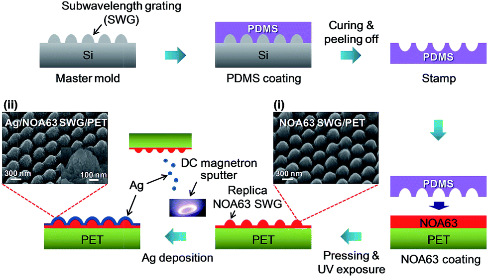
Fig. 1 shows the schematic diagram of the fabrication procedure for semi-transparent electrodes consisting of Ag/NOA63 SWG/PET. First, to fabricate the SWG patterned master molds, the single-polished (100) silicon (Si) was cleaned in acetone, methanol, and de-ionized water for 10 min, sequentially. As an etch mask, the photoresist (PR) was spin-coated on the Si substrate. After the prebaking, the samples were exposed twice to the argon laser while rotating the sample by 60 degree, followed by the development, creating two-dimensional (2D) hexagonal periodic dot PR arrays. Using the PR mask, finally, the SWG patterned Si molds were fabricated by inductively coupled plasma dry etching system, exhibiting the SWG height and period of ∼300 nm and ∼380 nm, respectively. The details of the fabrication method were described in our previous work.32 To transfer the SWG patterns onto the surface of PET substrates, the hard PDMS, formed by mixing and degassing four components (VDT-731, SIP 6831.1, SIT7900, and HMS-301 purchased from Gelest Inc.), was spin-coated on the Si mold and then cured in oven. Afterwards, the soft PDMS (base resin and curing agent, weight ratio = 10![[thin space (1/6-em)]](https://www.rsc.org/images/entities/char_2009.gif) :1) was covered on the hard PDMS/Si mold and cured again. Lastly, the negative SWG patterned PDMS stamp was obtained by separating the PDMS film from the Si mold. The NOA63 polymer was spin-coated on PET substrates at 3000 rpm for 1 min, and then immediately the samples were pressed with 3.0 kgf by the PDMS stamp. After UV exposure for 20 min, the SWGs on the surface of NOA63/PET were formed by peeling off the PDMS stamp, creating the NOA63 SWG/PET. As shown in the scanning electron microscope (SEM) image of Fig. 1(i), it is observed that the SWGs with 2D hexagonal periodic pattern arrays were well transferred on the NOA63 film/PET substrates without critical deformations and cracks, having the SWG height and period of ∼300 nm and ∼380 nm, respectively. After that, an Ag layer was deposited on the NOA63 SWG/PET by a DC magnetron sputtering system at 6 mTorr process pressure with 10 rpm rotation speed at room temperature for different Ag layer thicknesses of 10, 13, 17, 20, 25, and 35 nm, respectively. The deposition rate and argon flow rate were kept to be 0.2 nm s−1 and 30 sccm, respectively. From the SEM image of Fig. 1(ii), the Ag layer was successfully deposited on the NOA63 SWG/PET. For comparison, the Ag layer was also prepared on the flat bare PET substrates for each Ag layer thickness. For structural and morphological properties of the samples, a SEM (LEO SUPRA 55, Carl Zeiss) system was used. Their optical behaviors were investigated by using a UV-Vis-NIR spectrophotometer (Cary 5000, Varian). A spectroscopic ellipsometry (V-VASE, J. A. Woollam) was used for the measurement of angle-dependent optical properties at incident angles of 20–70° in non-polarized light. Electrical properties were also explored by using a Hall effect measurement system (Accent, HL5500PC).
:1) was covered on the hard PDMS/Si mold and cured again. Lastly, the negative SWG patterned PDMS stamp was obtained by separating the PDMS film from the Si mold. The NOA63 polymer was spin-coated on PET substrates at 3000 rpm for 1 min, and then immediately the samples were pressed with 3.0 kgf by the PDMS stamp. After UV exposure for 20 min, the SWGs on the surface of NOA63/PET were formed by peeling off the PDMS stamp, creating the NOA63 SWG/PET. As shown in the scanning electron microscope (SEM) image of Fig. 1(i), it is observed that the SWGs with 2D hexagonal periodic pattern arrays were well transferred on the NOA63 film/PET substrates without critical deformations and cracks, having the SWG height and period of ∼300 nm and ∼380 nm, respectively. After that, an Ag layer was deposited on the NOA63 SWG/PET by a DC magnetron sputtering system at 6 mTorr process pressure with 10 rpm rotation speed at room temperature for different Ag layer thicknesses of 10, 13, 17, 20, 25, and 35 nm, respectively. The deposition rate and argon flow rate were kept to be 0.2 nm s−1 and 30 sccm, respectively. From the SEM image of Fig. 1(ii), the Ag layer was successfully deposited on the NOA63 SWG/PET. For comparison, the Ag layer was also prepared on the flat bare PET substrates for each Ag layer thickness. For structural and morphological properties of the samples, a SEM (LEO SUPRA 55, Carl Zeiss) system was used. Their optical behaviors were investigated by using a UV-Vis-NIR spectrophotometer (Cary 5000, Varian). A spectroscopic ellipsometry (V-VASE, J. A. Woollam) was used for the measurement of angle-dependent optical properties at incident angles of 20–70° in non-polarized light. Electrical properties were also explored by using a Hall effect measurement system (Accent, HL5500PC).
 |
| | Fig. 1 Schematic diagram of the fabrication procedure for semi-transparent electrodes consisting of Ag/NOA63 SWG/PET. 40o-tilted SEM images of (i) NOA63 SWG/PET and (ii) Ag/NOA63 SWG/PET. | |
Numerical modelling and simulations
Optical analyses (i.e., reflection, transmission, near-field intensity distribution) of the semi-transparent electrodes consisting of Ag/NOA63 SWG/PET structure were carried out using a RCWA method in a commercial software package (DiffractMOD, Rsoft Design Group). For the numerical modeling, the SWGs were simply represented by a periodic geometry with a scalar-valued function of three variables, f(x,y,z), in a Cartesian coordinate system. Further details can be found in our previous work.30 The thicknesses of NOA63 polymer film and PET were set to be 1 and 200 μm, respectively. The refractive index and extinction coefficient of the PET and Ag used in these calculations were acquired from the index web site.33 For the NOA63 polymer film, the refractive index was assumed to be 1.56 while the extinction coefficient was not considered because it is negligible.25,34
Results and discussion
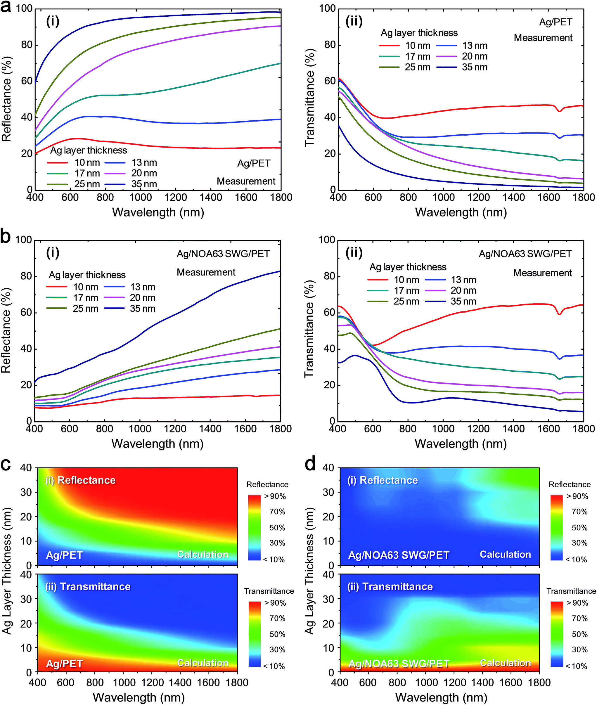
Fig. 2 shows the measured (i) reflectance and (ii) transmittance spectra of (a) Ag/PET and (b) Ag/NOA63 SWG/PET and the contour plots of variations of calculated (i) reflectance and (ii) transmittance spectra of (c) Ag/PET and (d) Ag/NOA63 SWG/PET for different Ag layer thicknesses in the wavelength (λ) range of 400–1800 nm. As shown in Fig. 2, the optical behaviors of Ag thin-film electrodes strongly depend on the Ag layer thickness. As the Ag layer thickness is increased, the reflectance is increased while the transmittance is decreased. However, from Fig. 2(a) and (b), the Ag/NOA63 SWG/PET has the lower reflectance spectrum and the higher transmittance spectrum at each Ag layer thickness compared to the Ag/PET. In the optical simulation results of Fig. 2(c) and (d), similarly, the Ag/NOA63 SWG/PET also shows a superior optical performance over a wide wavelength range of 400–1800 nm. This is attributed to the antireflective properties of the conical SWG structure on the surface NOA63 film/PET due to the linear effective gradient-refractive-index profile via the SWG with a period of 380 nm.32 Furthermore, the calculated results of both the samples with different Ag layer thicknesses exhibit a relatively reasonable agreement compared to the measured data in Fig. 2(a) and (b) though there is a slight discrepancy at some wavelengths. This may be the reason why it is difficult to exactly match the geometric simulation model to the experimentally fabricated structure and the mismatch of optical parameters (i.e., refractive index and extinction coefficient) for the constituent materials used in these experiments and calculations. The absorption spectra of both the samples were also estimated from 100 − reflectance − transmittance, as shown in Fig. S1 of the ESI.† Compared with the Ag/PET, the Ag/NOA63 SWG/PET shows larger absorption. This is mainly the SPR effect (i.e., strong electric and magnetic fields) around the Ag layer on NOA 63 SWGs.27–31 The SPR effect of the Ag/NOA63 SWG/PET will be covered in Fig. 5.
 |
| | Fig. 2 Measured (i) reflectance and (ii) transmittance spectra of (a) Ag/PET and (b) Ag/NOA63 SWG/PET and contour plots of variations of calculated (i) reflectance and (ii) transmittance spectra of (c) Ag/PET and (d) Ag/NOA63 SWG/PET for different Ag layer thicknesses at λ = 400–1800 nm. | |
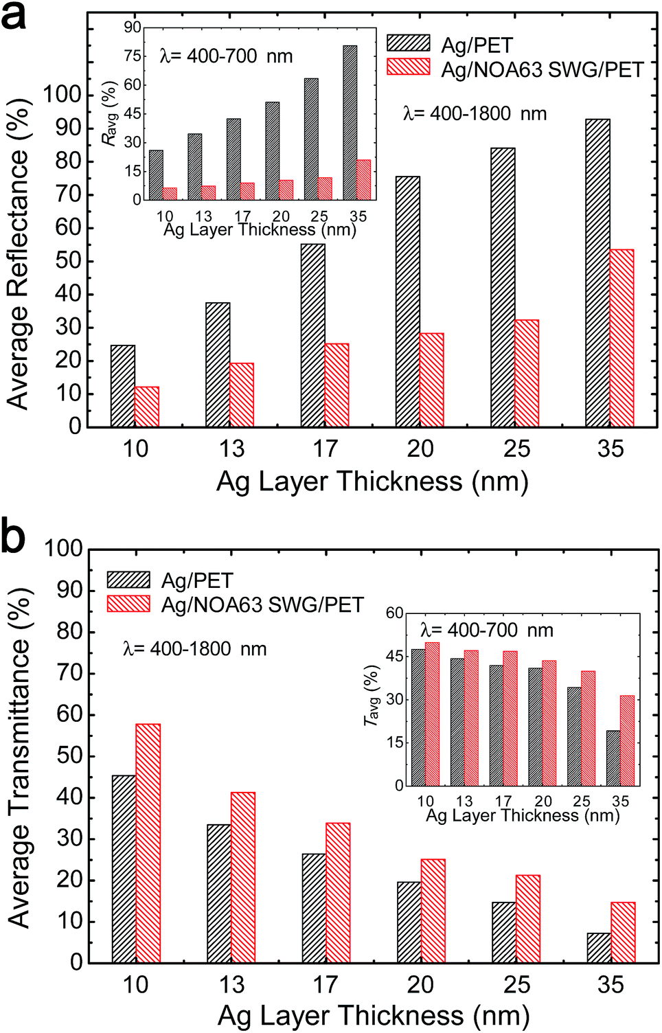
Fig. 3 shows the estimated (a) average reflectance (Ravg) and (b) average transmittance (Tavg) values of Ag/PET and Ag/NOA63 SWG/PET at λ = 400–1800 nm. For the corresponding samples, the estimated Ravg and Tavg values at visible wavelengths of 400–700 nm are also shown in the insets of Fig. 3(a) and (b), respectively. As can be seen in Fig. 3, the estimated Ravg and Tavg values are increased and decreased with increasing the Ag layer thickness, respectively. For the Ag/PET, as the Ag layer thickness is increased from 10 to 35 nm, the Ravg and Tavg values at λ = 400–1800 nm are increased from 24.7 to 92.8% and reduced from 45.3 to 7.2%, respectively. On the other hand, the Ag/NOA63 SWG/PET shows an improved optical property in both the reflectance and transmittance, exhibiting the variations from 12.2 to 53.5% in Ravg and from 57.5 to 14.7% in Tavg, respectively. In the visible wavelength region of 400–700 nm, the Ag/NOA63 SWG/PET has lower Ravg values of 6.3–20.9% and higher Tavg values of 48.4–31.5% compared to those (i.e., Ravg = 26–80.6% and Tavg = 47.5–19.2%) of the Ag/PET at Ag layer thicknesses of 10–35 nm, respectively.
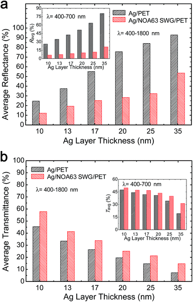 |
| | Fig. 3 Estimated (a) Ravg and (b) Tavg values of Ag/PET and Ag/NOA63 SWG/PET at λ = 400–1800 nm. The Ravg and Tavg values of the corresponding samples at λ = 400–700 nm are also shown in the insets of (a) and (b), respectively. | |
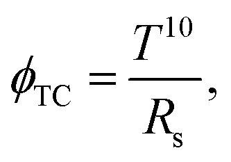
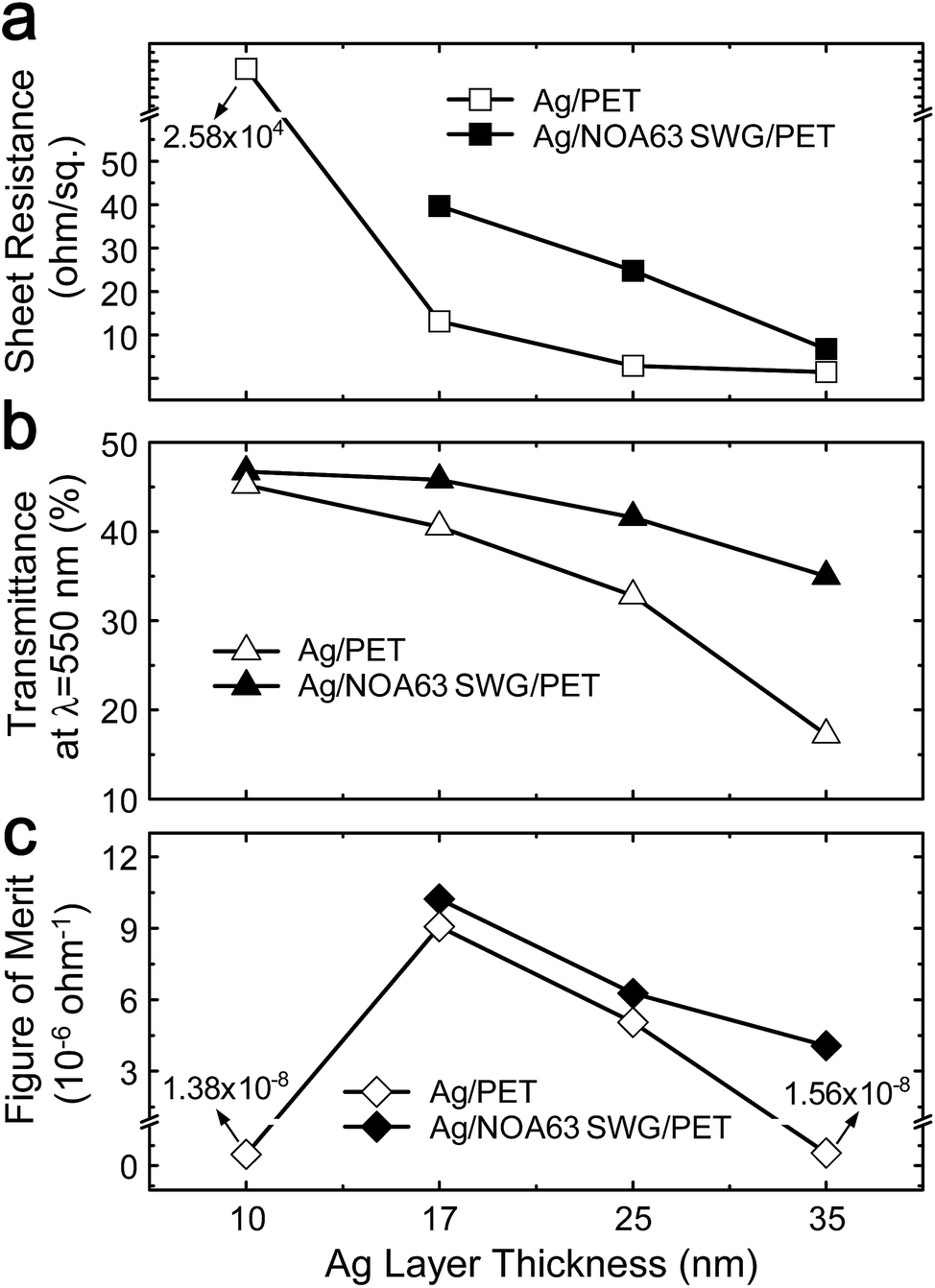
The electrical properties of Ag-coated nanostructured electrodes with different Ag layer thicknesses were also explored. Fig. 4 shows (a) sheet resistance (Rs), (b) transmittance at λ = 550 nm, and (c) figure of merit of Ag/PET and Ag/NOA63 SWG/PET as a function of the Ag layer thickness. As expected, the Rs value of both the samples is enhanced with increasing the Ag layer thickness from 10 to 35 nm. However, at the Ag layer thickness of 10 nm, the Ag/PET shows a very poor electrical property while there are no measured data for the Ag/NOA63 SWG/PET due to the thin Ag layer thickness. On the contrary, at the relatively thick Ag layer thickness of 35 nm, both the Ag/PET and Ag/NOA63 SWG/PET have good Rs values, exhibiting the Rs values of 1.45 and 6.77 ohm sq.−1, respectively. For both the samples, the transmittance values at λ = 550 nm in Fig. 4(b) were obtained from the transmittance spectra in Fig. 2. The transmittance value is decreased with increasing the Ag layer thickness. However, for the Ag/NOA63 SWG/PET, its transmittance is less dependent on the Ag layer thickness compared to the Ag/PET, exhibiting that it shows the relatively small variation in the transmittance from 46.7% at 10 nm to 35% at 35 nm while the Ag/PET has a considerable change in the transmittance from 45.2% at 10 nm to 17.2% at 35 nm. To determine the optimized condition among the Ag-coated nanostructured electrodes for different Ag layer thicknesses, the figure of merit (ϕTC) was estimated using the Rs and transmittance. The ϕTC is defined by Haacke as35
| |
 | (1) |
where
T is the transmittance at
λ = 550 nm and
Rs is the sheet resistance of the samples. As shown in
Fig. 4(c), both the samples show the maximum values at the Ag layer thickness of 17 nm. However, for the Ag/NOA63 SWG/PET, the higher
ϕTC value of 10.23 × 10
−6 ohm
−1 was obtained by two parameters of
T = 0.458 and
Rs = 39.71 ohm sq.
−1 compared to that (
i.e.,
ϕTC = 9.08 × 10
−6 ohm
−1,
T = 0.405 and
Rs = 13.08 ohm sq.
−1) of the Ag/PET. This Ag (17 nm)/NOA63 SWG/PET sample has
Tavg values of 46.9 and 33.9% and
Ravg values of 9 and 25.1% at
λ = 400–700 nm and 400–1800 nm, respectively, as can be seen in
Fig. 3(b). Especially, at visible wavelengths of 400–700 nm, this
Tavg (or
Ravg) value is relatively low (or high) compared to the commercial ITO films on glasses (
i.e.,
T > 80%,
Rs < 15 ohm sq.
−1)
36,37 and antireflective biomimetic nanostructured electrodes such as 3D ITO nanoparticles on ITO/AgO
x/ITO multilayer/PET (
i.e.,
T = 89%,
Rs = 65 ohm sq.
−1)
38 and ITO nanocolumns/GaAs (
i.e.,
R < 6%,
Rs = 50 ohm sq.
−1).
39 However, as mentioned above, the In is a rare earth metallic element, which causes the relatively high material cost of ITO. As an alternative of ITO, the antireflective biomimetic aluminum-doped zinc oxide (AZO) SWGs/film/Si structure was also reported in our group, exhibiting the
Ravg = 5% at
λ = 300–1100 nm and
Rs values of <30 ohm sq.
−1,
18 but the AZO SWGs/film electrodes were prepared by photolithography and dry etching processes with high fabrication cost and complexity. Furthermore, they also have large film thicknesses of >400 nm. These thick films are not suitable for flexible device applications since its brittleness causes cracks upon bending, including the additional thermal process at high temperatures of >200–300 °C. On the other hand, herein, the Ag/NOA63 SWG/PET is easily prepared by facile soft lithography and sputtering methods which make mass production possible. Besides, its
Rs value of 39.71 ohm sq.
−1 is similar or lower compared to the other commercial ITO films and nanostructured electrodes. Also, its
Tavg value at
λ = 400–700 nm is much higher than that (
i.e.,
Tavg = 25–30%) of electrodes used in semi-transparent photovoltaic devices in previous literatures.
40–42
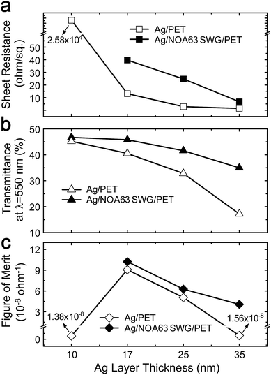 |
| | Fig. 4 (a) Sheet resistance, (b) transmittance at λ = 550 nm, and (c) figure of merit of Ag/PET and Ag/NOA63 SWG/PET as a function of the Ag layer thickness. | |
Fig. 5 shows (a) the photographs and (b) the contour plots of calculated electric (Ey) field intensity distributions of Ag/PET and Ag/NOA63 SWG/PET at the Ag layer thickness of 17 nm. As shown in Fig. 5(a), both the characters at the liquid crystal display (LCD) monitor and cellular phone camera are strongly reflected at the surface of the Ag/PET sample while there are almost no reflected ones on the surface of Ag/NOA63 SWG/PET sample. Additionally, the antireflective properties of SWGs can be also observed in the Ey field intensity distributions calculated by the RCWA simulation. In Fig. 5(b), for the Ag/PET, the Ey field intensity is high in the air region due to its strong reflection. For the Ag/NOA63 SWG/PET, on the other hand, there is a relatively weaker Ey field intensity in the air region (stronger Ey field intensity in the NOA63 region) due to its superior optical performance (i.e., antireflection) caused by the linear effective gradient-refractive-index profile via the SWG. Also, the metal thin-film electrodes with grating nanostructures can bring the enhanced light absorption in the active layer of optoelectronic devices (e.g., organic PVs or LEDs) due to the SPR effect (i.e., strong electric and magnetic fields) at the interface between the active and metal layers, which were generally proved by the calculated near-field intensity distributions in previous literatures.27–31 Similarly, the near-field intensity distributions of the Ag/NOA63 SWG/PET were calculated in Fig. S2 of the ESI.† The strong Ey or magnetic (Hy) fields around the Ag layer on NOA63 SWGs are observed at various wavelengths. Therefore, this SPR effect of Ag-coated NOA63 SWG electrodes can also boost the light absorption at the active layer in optoelectronic devices, thus leading to the enhancement of device performance.
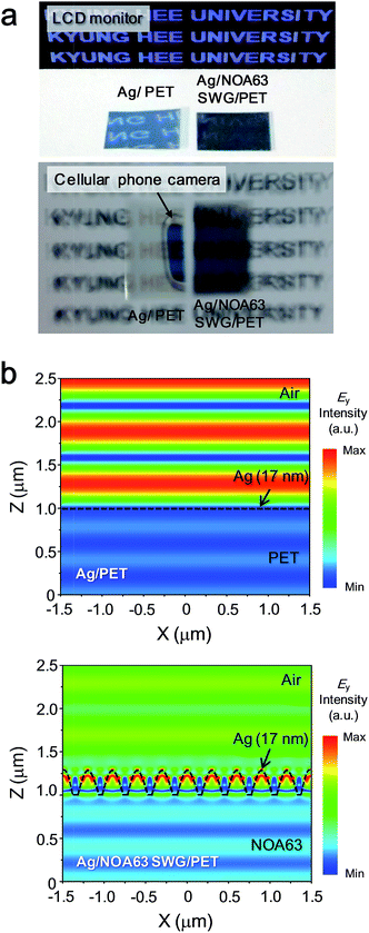 |
| | Fig. 5 (a) Photographs and (b) contour plots of calculated Ey field intensity distributions of Ag/PET and Ag/NOA63 SWG/PET at the Ag layer thickness of 17 nm. | |
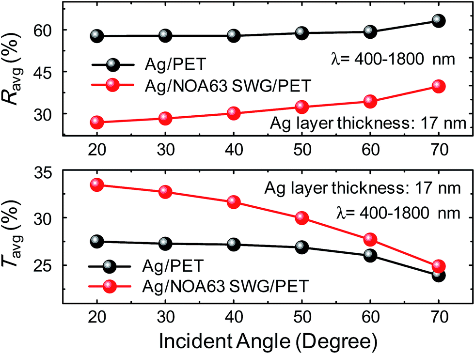
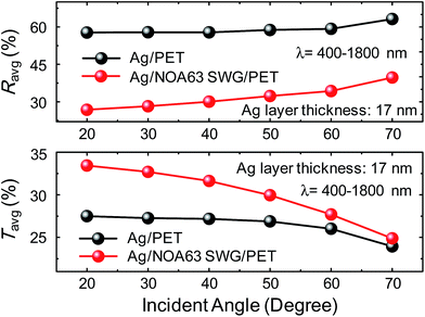
The angle-dependent optical property is also an important parameter to achieve high-performance optical and optoelectronic devices. Fig. 6 shows the Ravg and Tavg values of Ag/PET and Ag/NOA63 SWG/PET at the Ag layer thickness of 17 nm as a function of light incident angle under non-polarized light. For both the samples, as the incident angle is increased, the Ravg and Tavg values are gradually increased and decreased, respectively. However, for the Ag/NOA63 SWG/PET, the lower Ravg and higher Tavg values are still maintained from 26.8 to 39.7% in Ravg and from 33.4 to 24.9% in Tavg compared to those (i.e., Ravg = 57.8–63.1% and Tavg = 27.5–23.9%) of the Ag/PET in an incident angle range from 20 to 70°, exhibiting the lower Ravg = 31.9% and the larger Tavg = 30% at 20–70° (i.e., Ravg = 59.1% and the Tavg = 26.5% for the Ag/PET), respectively.
 |
| | Fig. 6 Ravg and Tavg values of Ag/PET and Ag/NOA63 SWG/PET at the Ag layer thickness of 17 nm as a function of light incident angle under non-polarized light. | |
Conclusions
The metal thin-film nanostructured electrodes consisting of the Ag/NOA63 SWG/PET were fabricated by the soft lithography via both the PDMS stamps and Si molds and the subsequent sputtering. The optical (i.e., reflection, transmission, and absorption) and electrical (i.e., sheet resistance) properties of the Ag/NOA63 SWG/PET were strongly dependent on the Ag layer thickness. The Ag (17 nm)/NOA63 SWG/PET with the maximum ϕTC value of 10.23 × 10⁻⁶ ohm−1 (i.e., T = 0.458 at λ = 550 nm and Rs = 39.71 ohm sq.−1) showed the lower Ravg and larger Tavg values in the broad wavelength range of 400–1800 nm, respectively. The theoretically calculated optical results showed a similar tendency to the experimentally measured data. The strong Ey or Hy fields (i.e., SPR effect) were observed around the Ag layer on NOA63 SWGs for different wavelengths. It also exhibited less-angle dependent optical characteristics compared to the Ag/PET at incident angles of 20–70°. These results can provide a better insight into the semi-transparent metal electrodes consisting of polymer SWGs, which can be simply prepared by the facile, mass-productive, and cost-effective soft lithography, with the broadband and wide-angle antireflection as well as the good electrical property including the SPR effect for high-performance optical and optoelectronic device applications.
Acknowledgements
This work was supported by the National Research Foundation of Korea (NRF) grant funded by the Korea government (MSIP) (No. 2014-069441).
References
- C. C. Chen, L. Dou, J. Gao, W. H. Chang, G. Li and Y. Yang, Energy Environ. Sci., 2013, 6, 2714 CAS.
- M. G. Kang and L. J. Guo, Adv. Mater., 2007, 19, 1391 CrossRef CAS PubMed.
- S. K. Chang-Jian, J. R. Ho and J. W. J. Cheng, Opt. Laser Technol., 2011, 43, 1371 CrossRef CAS PubMed.
- J. Lee, D. K. Hwang, J. M. Choi, K. Lee, J. H. Kim, S. Im, J. H. Park and E. Kim, Appl. Phys. Lett., 2005, 87, 023504 CrossRef PubMed.
- W. Nie, H. Tsai, R. Asadpour, J. Blancon, A. J. Neukirch, G. Gupta, J. J. Crochet, M. Chhowalla, S. Tretiak, M. A. Alam, H. L. Wang and A. D. Mohite, Science, 2015, 347, 522 CrossRef CAS PubMed.
- Y. Yang, Y. Zheng, W. Cao, A. Titov, J. Hyvonen, J. R. Manders, J. Xue, P. H. Holloway and L. Qian, Nat. Photonics, 2015, 9, 259 CAS.
- B. Winther-Jensen and F. C. Krebs, Sol. Energy Mater. Sol. Cells, 2006, 90, 123 CrossRef CAS PubMed.
- L. Hu, H. S. Kim, J. Y. Lee, P. Peumans and Y. Cui, ACS Nano, 2010, 4, 2955 CrossRef CAS PubMed.
- Y. H. Kim, L. Müller-Meskamp, A. A. Zakhidov, C. Sachse, J. Meiss, J. Bikova, A. Cook, A. A. Zakhidov and K. Leo, Sol. Energy Mater. Sol. Cells, 2012, 96, 244 CrossRef CAS PubMed.
- Y. Y. Lee, K. H. Tu, C. C. Yu, S. S. Li, J. Y. Hwang, C. C. Lin, K. H. Chen, L. C. Chen, H. L. Chen and C. W. Chen, ACS Nano, 2011, 5, 6564 CrossRef CAS PubMed.
- M. Fahland, P. Karlsson and C. Charton, Thin Solid Films, 2001, 392, 334 CrossRef CAS.
- K. Ellmer, Nat. Photonics, 2012, 6, 809 CrossRef CAS PubMed.
- D. S. Hecht, L. Hu and G. Irvin, Adv. Mater., 2011, 23, 1482 CrossRef CAS PubMed.
- F. Galeotti, F. Trespidi, G. Timò and M. Pasini, ACS Appl. Mater. Interfaces, 2014, 6, 5827 CAS.
- K. Forberich, G. Dennler, M. C. Scharber, K. Hingerl, T. Fromherz and C. J. Brabec, Thin Solid Films, 2008, 516, 7167 CrossRef CAS PubMed.
- D. H. Ko, J. R. Tumbleston, K. J. Henderson, L. E. Euliss, J. M. DeSimone, R. Lopez and E. T. Samulski, Soft Matter, 2011, 7, 6404 RSC.
- D. G. Stavenga, S. Foletti, G. Palasantzas and K. Arikawa, Proc. R. Soc. B, 2006, 273, 661 CrossRef CAS PubMed.
- J. W. Leem, D. H. Joo and J. S. Yu, Sol. Energy Mater. Sol. Cells, 2011, 95, 2221 CrossRef CAS PubMed.
- Y. Xia and G. M. Whitesides, Annu. Rev. Mater. Sci., 1998, 28, 153 CrossRef CAS.
- T. W. Odom, J. C. Love, D. B. Wolfe, K. E. Paul and G. M. Whitesides, Langmuir, 2002, 18, 5314 CrossRef CAS.
- S. H. Ahn and L. J. Guo, ACS Nano, 2009, 3, 2304 CrossRef CAS PubMed.
- Y. M. Song, Y. Xie, V. Malyarchuk, J. Xiao, I. Jung, K. J. Choi, Z. Liu, H. Park, C. Lu, R. H. Kim, R. Li, K. B. Crozier, Y. Huang and J. A. Rogers, Nature, 2013, 497, 95 CrossRef CAS PubMed.
- J. W. Leem, M. Choi and J. S. Yu, ACS Appl. Mater. Interfaces, 2015, 7, 2349 CAS.
- C. S. Huang, E. Y. B. Pun and W. C. Wang, J. Opt. Soc. Am. B, 2009, 26, 1256 CrossRef CAS.
- J. W. Leem, X. Y. Guan, M. Choi and J. S. Yu, Sol. Energy Mater. Sol. Cells, 2015, 134, 45 CrossRef CAS PubMed.
- S. Y. Heo, J. K. Koh, G. Kang, S. H. Ahn, W. S. Chi, K. Kim and J. H. Kim, Adv. Energy Mater., 2014, 4, 1300632 Search PubMed.
- X. H. Li, W. E. I. Sha, W. C. H. Choy, D. S. S. Fung and F. X. Xie, J. Phys. Chem. C, 2012, 116, 7200 CAS.
- X. Li, W. C. H. Choy, L. Huo, F. Xie, W. E. I. Sha, B. Ding, X. Guo, Y. Li, J. Hou, J. You and Y. Yang, Adv. Mater., 2012, 24, 3046 CrossRef CAS PubMed.
- J. D. Chen, L. Zhou, Q. D. Ou, Y. Q. Li, S. Shen, S. T. Lee and J. X. Tang, Adv. Energy Mater., 2014, 4, 1301777 Search PubMed.
- J. W. Leem, S. Kim, C. Park, E. Kim and J. S. Yu, ACS Appl. Mater. Interfaces, 2015, 7, 6706 CAS.
- Y. G. Bi, J. Feng, Y. F. Li, X. L. Zhang, Y. F. Liu, Y. Jin and H. B. Sun, Adv. Mater., 2013, 25, 6969 CrossRef CAS PubMed.
- J. W. Leem, Y. M. Song, Y. T. Lee and J. S. Yu, Appl. Phys. B, 2010, 100, 891 CrossRef CAS.
- Filmetrics Refractive index database (2015), retrieved 2015, http://www.filmetrics.com.
- Norland Optical Adhesive (2015), retrieved 2015, https://www.norlandprod.com.
- G. Haacke, J. Appl. Phys., 1976, 47, 4086 CrossRef CAS PubMed.
- D. Paeng, J. H. Yoo, J. Yeo, D. Lee, E. Kim, S. H. Ko and C. P. Grigoropoulos, Adv. Mater., 2015, 27, 2762 CrossRef CAS PubMed.
- R. Pandey, C. H. Wie, X. Lin, J. W. Lim, K. K. Kim, D. K. Hwang and W. K. Choi, Sol. Energy Mater. Sol. Cells, 2015, 134, 5 CrossRef CAS PubMed.
- W. Wang, T. S. Bae, Y. H. Park, D. H. Kim, S. Lee, G. Min, G. H. Lee, M. Song and J. Yun, Nanoscale, 2014, 6, 6911 RSC.
- P. Yu, C. H. Chang, C. H. Chiu, C. S. Yang, J. C. Yu, H. C. Kuo, S. H. Hsu and Y. C. Chang, Adv. Mater., 2009, 21, 1618 CrossRef CAS PubMed.
- C. Roldán-Carmona, O. Malinkiewicz, R. Betancur, G. Longo, C. Momblona, O. Malinkiewicz, R. Betancur, G. Longo and C. Momblona, Energy Environ. Sci., 2014, 7, 2968 Search PubMed.
- K. S. Chen, J. F. Salinas, H. L. Yip, L. J. Huo, J. H. Hou and A. K. Y. Jen, Energy Environ. Sci., 2012, 5, 9551 CAS.
- C. C. Chueh, S. C. Chien, H. L. Yip, J. F. Salinas, C. Z. Li, K. S. Chen, F. C. Chen, W. C. Chen and A. K. Y. Jen, Adv. Energy Mater., 2013, 3, 417 CrossRef CAS PubMed.
Footnote |
| † Electronic supplementary information (ESI) available: Absorption of the samples and calculated near-field intensity distribution of Ag/NOA63 SWG/PET at different wavelengths. See DOI: 10.1039/c5ra14282b |
|
| This journal is © The Royal Society of Chemistry 2015 |
Click here to see how this site uses Cookies. View our privacy policy here. 
 Open Access Article
 This Open Access Article is licensed under a