High sensitivity of a carbon nanowall-based sensor for detection of organic vapours

P. Slobodian*a, U. Cvelbar*b, P. Rihac, R. Olejnika, J. Matyasa, G. Filipičb, H. Watanabed, S. Tajimad, H. Kondod, M. Sekined and M. Horid
aCentre of Polymer Systems, University Institute, Tomas Bata University, Trida T. Bati 5678, 760 01 Zlin, Czech Republic
bDepartment F4, Jozef Stefan Institute, Jamova cesta 39, SI-1000 Ljubljana, Slovenia
cInstitute of Hydrodynamics, Academy of Sciences, 166 12 Prague, Czech Republic
dPlasma Nanotechnology Research Center (PLANT), Graduate School of Engineering, Nagoya University, Furo-cho Chikusa-ku, Nagoya 464-8603, Japan. E-mail: slobodian@cps.utb.cz; uros.cvelbar@ijs.si

Received 22nd June 2015 , Accepted 15th October 2015

First published on 15th October 2015


Abstract

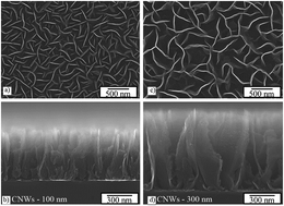
The high sensitivity in response, selectivity and reversibility was achieved on a carbon nanowall-based sensor for the vapor detection of volatile organic compounds, which were tested by an electrical resistance method during adsorption and desorption cycles. The maze-like structure of two different carbon nanowalls with wall-to-wall distances of 100 nm and 300 nm were prepared on a silicone substrate by a plasma-enhanced chemical vapor deposition system while varying processing parameters. Four organic vapors: iso-pentane; diethyl ether; acetone; and methanol; were selected in order to evaluate the relationship between the change in resistance, molecular weight of the adsorbent and the polarity. The results show that the carbon nanowalls with average wall distance 100 nm exhibit substantially enhanced electrical response to all volatile organic compound vapors used in comparison with the nanowalls with 300 nm wall distance as well as entangled multiwall carbon nanotube networks.


Introduction

Carbon nanowalls (CNWs) represent a two-dimensional wall-like carbon nanostructure of aligned and well-separated graphene sheets.1 CNWs are predominantly synthesized by chemical vapor deposition (CVD) or more specifically by plasma enhanced chemical vapor deposition (PECVD). These preparation methods include various plasma enhanced methods specified by generation of a discharge ranging from microwave (MW-PECVD), inductively coupled (IC-PECVD), capacitively coupled (CC-PECVD), electron-beam (EB-PECVD), hot filament PECVD, atmospheric pressure plasma synthesis or even sputtering processes.1–4 In most cases there is no need for a metal catalyst, where growth is successfully realized at low temperatures of around 500 to 700 °C on various substrates including silicon, oxides, metals or even organic substances by simply generating carbon building blocks in hydrocarbons (e.g. CH4,…) or fluorocarbons (e.g. CF4, C2F6,…) containing gas flow mixtures with hydrogen.4–7 As in our case, where they are prepared by using a plasma-enhanced chemical vapor deposition (PECVD), during which CNWs are self-organized on a flat silicon oxide substrate and pointed radially outward where walls terminate into open graphitic edge planes and sheets on top. CNWs distribution is usually uniform over the whole substrate with wall thickness in the range of ∼30–50 nm3 or ∼15–20 nm2 with constantly decreasing number of graphene layers in the axial growth direction. At the wall top only 1–3 graphene layers are observed by TEM analysis. The density of CNWs (number of CNWs per unit length) can be controlled by varying processing parameters such as the total pressure and the power.4 Final CNW structure is assembled into inter-connected and self-supported three-dimensional network of graphene nanosheets5–7 with the most common morphological maze-like structure.4,6 The network contains junctions, where one nanosheet is terminated by the other nanosheet. With increasing grown time, the degree of interlinking increases together with the wall height.1 The nano-wall network is electro-conductive with semiconductor properties. One of the important factors influencing the conductivity of graphene nanowalls is the density of defects and voids.6 In the case of pure and undoped CNWs, p-type conduction is supposed because the majority conduction carriers are presumably positive holes since mobile π electrons would be easily trapped by the defects.5,6 But the total conductivity of CNW network is mainly affected by the resistance of contacts between individual graphene sheets constituting the wall and then by the contact resistance in the nanowall junctions and their density.4,8 It was demonstrated in the previous paper that the conductivity of CNW films can be controlled by varying CNW density, which can be controlled by the process parameters as the total pressure and power while maintaining the same crystal quality.4 However, one may also suppose that morphology of CNW edges and distances between individual graphene nanosheets in junctions affecting the probability for electron hopping or tunneling can vary macroscopic electrical properties.6

So far, very little is known about sensing properties of CNW for volatile organic vapors (VOC's). For this reason one has to look around other carbon-based materials such as carbon nanotubes (CNTs)9–12 and graphene13,14 which have been effectively used for gas sensing applications. However some work was reported for CNW as gas sensing applications, which are interesting especially due to large surface area. CNW film was already successfully used for detection of NO2 and NH3 at room temperature since NO2 lowers and NH3 raises the film resistance.15 CNW film behaves like a p-type semiconductor when NO2 increases the concentration of holes while adsorption of NH3 molecules on CNW surface means a decreased majority of carrier holes concentration. NO2 and NH3 were also used to test gas sensing ability of a field-effect transistor (FET) sensor prepared as the patterned graphene sheets bridging a metal electrode gap.13 More works were reported for the entangled multiwall carbon nanotube network (buckypaper) for detection of organic solvent vapors through the electrical resistance measurement.9,10,13,17 The electrical resistance variation as a response to physisorption and desorption of vapors from carbon nanotubes during cycles was found to be reversible, reproducible, sensitive and selective. The possible mechanism of resistance change involves mainly the formation of non-conducting layers on nanotubes which affects the resistance of intertube contacts and thus the conductivity of the MWCNT network. Furthermore many other types of materials were successfully used for VOC detection, for instance, the electrically conductive polyaniline18 or polymer nanocomposites with carbon black19 as well as the conventional type of sensors based on inorganic semiconducting materials.19–22 The conventional sensors have a higher sensitivity than carbon-base ones. On the other hand, the former ones has to be preheated to an elevated temperature in order to increase probability of gas molecule adsorption while the latter operate at room temperature.

In this study, we use carbon nanowalls-based sensor for detection of VOC vapors in air at room temperature using the electrical resistance method. The selectivity, reversibility and the sensor response to vapors of different polarities, given by Hansen solubility parameters, and volume fraction of saturated vapor during adsorption/desorption cycles are evaluated and discussed.

Experimental

CNW sample preparation

The experimental setup used in this study is described in details elsewhere.23,24 The system consists of surface wave plasma (SWP) region driven by a 2.45 GHz microwave power supply to generate H atoms and a capacitively coupled plasma (CCP) region generated by a 100 MHz power supply to fabricate nanowalls from CH4 gas. The high density H atoms were generated at the top of the PECVD system by the SWP system which was operated at 2.54 GHz and injection into the PECVD system. Uniform CNWs in the area of 25 cm2 were observed in the CCP region.

CNWs were deposited on the thermally grown SiO2 film on a Si p-type (100) wafer. The uniqueness of aforementioned PECVD apparatus is that H and CH density can be separately controlled in two plasma regions. Variation of experimental conditions leads to different average distance between adjacent CNWs, see Table 1. The flow rate of H2 and carbon (CH4) gases were 50 and 100 sccm, respectively. The microwave power was kept at 400 W throughout the experiment. In order to fabricate CNW with the wall-to-wall distance of 100 nm and 300 nm, the 100 MHz power supply was changed from 100 W to 500 W. The process pressure was 1 Pa for CNWs (100 nm) or 5 Pa for CNWs (500 nm) and growth time 60 min or 10 min, respectively. The substrate was heated in the CCP chamber to 600 °C during deposition using a carbon heater. The detail process conditions are summarized in Table 1.

Table 1 Process conditions and results of analyses of both principal tested CNWs (100 nm) and CNWs (300 nm)
Average gap between each CNWs [nm] 100 300
Average height of CNWs [nm] 650 970
Conductivity [S cm−1] 38 76
Process pressure [Pa] 1 5
Substrate temperature [°C] 600 600
SWP power [W] 400 400
CCP power [W] 100 500
H2 [sccm][thin space (1/6-em)]:[thin space (1/6-em)]CH4 [sccm] 50[thin space (1/6-em)]:[thin space (1/6-em)]100 50[thin space (1/6-em)]:[thin space (1/6-em)]100
Growth time [min] 60 10


Characterization of CNWs

Scanning electron microscope (S-5200 Hitachi High-Technologies Corporation, Japan) was used to observe the surface morphology of CNWs. The crystallinity of carbon nanowalls was determined from Raman spectroscopy (inVia, Renishaw plc, United Kingdom). Each Raman band was analyzed by fitting with a Lorentzian line. Peaks are located at around 1350 cm−1 for D band (disordered induced peak), 1580 cm−1 for G band (graphite peak), 1620−1 cm for D′ band (symmetry breaking due to finite sp2 crystalline size), 2700 cm−1 for 2D (G′) band (second order of the D peak, appearance of this peak is treated as a fingerprint of crystalline of carbon materials) and 2950 cm−1 for D + G (D′′) band (combination band of D and G peaks). Intensity ratio of the D and G peaks, ID/IG indicates that size of crystalline grains as well as the inter defect distance.16

Electrical resistance measurements

The electrical resistance of a wafer with grown CNWs was measured by the two-point technique using a multimeter (Sefram 7338, France). The wafer was placed on a planar holder with Cu electrodes fixed to it by a silver colloid electro-conductive paste (Dotite D-550, SPI Supplies, USA). The holder was placed into the thermostatic box with the temperature 25 °C and relative humidity 60%. Time-dependent electrical resistance measurement was performed during adsorption and desorption cycles. The holder with the specimen was quickly transferred into an airtight conical flask full of vapors of the respective solvent (iso-pentane, diethyl ether, acetone and methanol) a layer of which was at the bottom.9,10,16,25–27 After 15 minutes of measurement the holder was promptly removed from the flask, and for the next 15 minutes the sample was measured in the mode of desorption. This was repeated in fourth consecutive cycles.

Results and discussion

Two kinds of CNWs with wall-to-wall spacing of 100 nm and 300 nm were successfully grown on the SiO2–Si substrate and the representative cross-sectional SEM images are shown in Fig. 1 that show the well-separated vertically standing graphene sheets with uniform distribution and maze-like structure. The thicknesses of individual CNW sheets were approximately ∼15–35 nm and ∼20–40 nm for CNWs (100 nm) and CNWs (300 nm), respectively. The height of CNWs (100 nm) was approximately 650 nm and 970 nm in case of CNWs (300 nm). The electrical conductivity of CNWs is proportional to the number of CNWs per unit length.3 The electrical conductivity of CNWs were ∼38 S cm−1 for 100 nm wall-to-wall spacing and ∼76 S cm−1 for 300 nm wall-to-wall spacing. This indicated that the conductivity of CNWs in S cm−1 is proportional to the density of CNWs, which showed the opposite trend described in ref. 4. However, the detailed comparison of our results with the previous ones (ref. 4) shows that according to the experimental arrangement, that is, the total pressure and VHF power, the setting of the experimental setup 1 Pa/100 W for CNWs (100 nm) produces explicably less conductive CNWs that the setting 5 Pa/500 W for CNWs (300 nm). The Raman spectra help to explain these results, see Fig. 2 and Table 2. Namely, the deposition conditions in ref. 3 did not change the intensity ratio of the D and G peaks, ID/IG, indicating no change in the crystal quality in comparison with the present results. Higher ID/IG ratio for CNWs (100 nm) in comparison with CNWs (300 nm) can be attributed to more defects in crystalline structure due to the larger portion of graphitized edge planes.28 The higher portion of nano-crystalline graphitic components can be explained also by a shift of G-peak from 1581 cm−1 for CNWs (300 nm) to 1597 cm−1 for CNWs (100 nm).29 One can suppose that the top morphology of CNWs edges affects conducting properties. Irrespective of that CNWs (100 nm) are denser and have more inter-contacts between individual graphene nanosheet, what should enhance macroscopic electrical conductance, the defective structure and the higher fraction of graphitized edges results in a lower conductance. The contacts between individual graphene sheets act as resistors in the conductive CNWs network. The resulting overall CNW resistance is apparently higher for CNWs (100 nm) than for CNWs (300 nm). Also higher wall thickness of CNWs (300 nm) may increase the conductivity.
image file: c5ra12000d-f1.tif
Fig. 1 SEM micrographs of upper surface and cross-section of CNWs. Parts (a) and (b) CNWs with average wall distance 100 nm, parts (c) and (d) CNWs with average wall distance 300 nm.

image file: c5ra12000d-f2.tif
Fig. 2 Raman spectra for (a) CNWs (100 nm) and (b) CNWs (300 nm).
Table 2 ID/IG, ID′/IG, I2D/IG ratios and the position of peaks of Raman spectra for both tested CNWs
Sample

image file: c5ra12000d-t1.tif

image file: c5ra12000d-t2.tif

image file: c5ra12000d-t3.tif

λD [cm−1] λG [cm−1] λD′ [cm−1] λ2D [cm−1]
CNWs – 100 nm 2.29 0.91 0.40 1357 1597 1624 2693
CNWs – 300 nm 2.04 0.84 0.45 1334 1581 1607 2684


Since CNW have high surface-to-volume ratio they are applicable for detection of VOC in air, which would lead to considerable decrease of macroscopic conductance. The molecules are adsorbed on CNW surface by van der Waals attracting forces what increases electric resistance of inter-wall contacts. The process of adsorption/desorption is reversible and selective to different kind of molecules as follows from Fig. 3. One cycle of the adsorption/desorption resistance response of both tested CNW networks to four different solvents which vary in concentration of their saturated vapors in air and cover a broad range of polarities defined by Hansen solubility parameters shows differences between two types of CNWs. The properties of solvents, that is, iso-pentane (i-PE), diethyl ether (DEE), acetone (AC) and methanol (Me–OH) are summarized in Table 3. Hansen solubility parameters are defined by eqn (1),

 
δt2 = δd2 + δp2 + δh2, (1)
where δt is the total Hildebrand solubility parameter, δd, δp and δh denote dispersion, polar and hydrogen bonding component, respectively. The saturated vapor pressures, pi, of individual solvents are also given in Table 3, as well as the corresponding volume fractions, xi. These are determined as,
 
image file: c5ra12000d-t4.tif(2)
where pA represents air pressure. As the table shows, pi of the solvents systematically decreases with increasing δt.


image file: c5ra12000d-f3.tif
Fig. 3 One adsorption/desorption cycle for CNWs (a) 100 nm and (b) 300 nm exposed to vapors of iso-pentane, diethyl ether, acetone and methanol.
Table 3 Properties of used organic solvents: Hansen solubility parameters δd, δp, δd, the total Hildebrand solubility parameter δt, the saturated vapor pressures pi, the corresponding volume fraction xi, of solvents at 25 °C and at atmospheric pressure further expressed as thousands of ppm
Solvent δd/δp/δh [MPa1/2] δt [MPa1/2] pi [kPa] xi [vol%] [103 ppm]
iso-Pentane (i-PE) 13.7/0/0 13.7 91.37 90.2, 902
Diethyl ether (DEE) 14.5/2.9/5.1 15.6 70.9 70.9, 709
Acetone (AC) 15.5/10.4/7.0 20.0 30.46 30.1, 301
Methanol (Me–OH) 15.1/12.3/22.3 29.6 16.76 16.5, 165


The first part of Fig. 3 shows the resistance measurement for CNWs (100 nm). At the start of adsorption, the initial sharp increase of the value of parameter S, the sensor response, is observed followed by a slower phase. The sensor response S is defined as,

 
image file: c5ra12000d-t5.tif(3)
where Ra represents the specimen resistance in air and Rg the resistance of specimen exposed to vapor, ΔR stands for the resistance change. In the course of desorption the organic molecules are removed from CNW surface and the specimen resistance recovers. Desorption phase starts again by a rapid sensor response decrease followed by a slower approach to a constant value within time of the cycle.

The comparison of CNW results with adsorption of the same set of solvents on multiwall carbon nanotube (MWCNT) networks9 shows the CNWs (100 nm) have significantly higher sensor responses. Particularly, the sensor response value for DEE is twelve times higher than the corresponding value for MWCNT network made of KMnO4 oxidized nanotubes. On the other hand, the sensor response value for CNWs (300 nm) is significantly lower for all used solvents and comparable with previous results for MWCNT. However, the selectivity to solvents differs from the one for MWCNT networks. The comparison of CNWs and MWCNT KMnO4 oxidized network response to adsorption of all tested VOC is summarized in Table 4.

Table 4 The values of sensor responses of CNWs exposed to the saturated vapors of four different organic solvents at the end of the first 15 min adsorption cycle and the corresponding results for MWCNT network oxidized by KMnO4 (ref. 9)
Solvent S – 100 nm [%] S – 300 nm [%] S – MWCNT(KMnO4) [%]
iso-Pentane 65.4 8.5 12.0
Diethyl ether 327.1 36.2 27.2
Acetone 273.8 24.9 34.1
Methanol 87.2 16.9 46.6


The maximum resistance, which indicates the VOC adsorption, of CNWs (100 nm) was higher compared to CNWs (300 nm) for all solvents. This could be explained by several reasons. Firstly, CNWs 100 nm are capable to adsorb more vapor of analyte into CNWs structure because of the higher average surface area and thus higher number of inter-wall contacts and the overall resistance increase. Secondly, it can be assumed the higher fraction of graphitized edges with already higher initial contact resistance of junctions compared with CNWs (300 nm), which probably lose electrical contacts due to the presence of adsorbed molecules more easily.

Fig. 4 shows the response CNW (100 nm) to the four solvent vapors in four consecutive adsorption/desorption cycles. The responses for all solvents are reversible with irreversible part of the resistance change about 7–14% depending on the analyte. Sensor response for DEE and acetone slightly increases with the number of cycles. This is probably due to not complete desorption of the analyte after the previous cycle.


image file: c5ra12000d-f4.tif
Fig. 4 Four consecutive adsorption/desorption cycles for CNWs (100) exposed to vapors of iso-pentane (○), diethyl ether (△), acetone (□) and methanol (◇).

The higher selectivity of CNWs (100 nm) over CNWs (300 nm) in terms of the dependence of the sensor response divided by the saturated vapor pressure, pi, on polarity defined by the total Hildebrand solubility parameter, δt is clearly seen from Fig. 5. The selectivity of CNWs (100 nm) increases with polarity from iso-pentane over DEE to the maximum value for acetone and drops for methanol. However, the selectivity has only slightly increasing trend with polarity in case of less sensitive CNWs (300 nm). The presented results for CNWs (100 nm) are promising from the point of view of practical applications of CNWs for vapor detection. Different sensitive materials are very valuable for the concept of a special analytical device called electronic nose.27 The idea is to use simultaneously a set of different sensors with selective responses which may analyze unknown vapor sample according to the database of responses.


image file: c5ra12000d-f5.tif
Fig. 5 Dependence of sensor response S divided by the saturated vapor pressure pi on the solvent polarity defined by the total Hildebrand solubility parameter δt.

Conclusions

The carbon nanowall-based sensor with average wall distance 100 nm has substantially enhanced electrical resistance response to vapors of volatile organic compounds in comparison with CNWs (300 nm) and MWCNT networks. The mechanism of macroscopic resistance increase may be explained by formation of a non-conducting layer in the contact between nano-walls. With regard to the high number of inter-wall contacts of the dense CNWs (100 nm), the high resistance increase after the vapor adsorption seems corresponding. The selective detection of CNWs (100 nm) is strong for acetone, slightly less for DEE and low for two opposite cases, namely, the polar methanol and the non-polar iso-pentane. The sensing properties of CNWs can be controlled by the processing parameters, the total pressure and the discharge power during CNWs growth. The adsorption of solvents covering a broad range of polarities determines CNWs properties which are suitable for the application as cheap and easy to prepare vapor sensor arrays which are selective and have reversible and reproducible properties.

Acknowledgements

This work was supported by the Ministry of Education, Youth and Sports of the Czech Republic – Program NPU I (LO1504). P.R. would like thank to support by the Fund of Institute of Hydrodynamics AV0Z20600510. U.C. and G.F. would gratefully like to acknowledge financial support from Slovenian Research Agency (ARRS) grant L2-6769 and Bi-JAP-2015-2017-3. S. T., H. K., M. S., and M. H. would acknowledge the Japan Society for the Promotion of Science (JSPS) Bilateral Joint Research Projects/Seminars, and S. T. was partially supported by JSPS Grant-in-Aid for Exploratory Research (KAKENHI Houga) grant. no. 25600123.

References

  1. M. Hiramatsu and M. Hori, Carbon Nanowalls, Springer, 2010, pp. 9–28 Search PubMed.
  2. N. Soin, S. S. Roy, C. O'Kane, J. A. D. McLaughlin, T. H. Limb and C. J. D. Hetherington, CrystEngComm, 2011, 13, 312 RSC.
  3. A. T. H. Chuang, B. O. Boskovic and J. Robertson, Diamond Relat. Mater., 2012, 15, 1103 CrossRef PubMed.
  4. H. J. Cho, H. Kondo, K. Ishikawa, M. Sekine, M. Hirarnatsu and M. Hori, Carbon, 2014, 68, 380 CrossRef CAS PubMed.
  5. Y. H. Wu, P. W. Qiao, T. C. Chong and Z. X. Shen, Adv. Mater., 2002, 14, 64 CrossRef CAS.
  6. D. H. Seo, S. Kumar and K. Ostrikov, Carbon, 2011, 49, 4331 CrossRef CAS PubMed.
  7. W. Takeuchi, M. Ura, M. Hiramatsu, Y. Tokuda and H. M. Hori, Appl. Phys. Lett., 2008, 92, 213103 CrossRef PubMed.
  8. Y. H. Wu, B. J. Yang, B. Y. Zong, H. Sun, Z. X. Shen and Y. P. Feng, J. Mater. Chem., 2004, 14, 469 RSC.
  9. L. Niu, Y. L. Luo and Z. Q. Li, Sens. Actuators, B, 2007, 126, 361 CrossRef CAS PubMed.
  10. P. Slobodian, P. Riha, A. Lengalova, P. Svoboda and P. Saha, Carbon, 2011, 49, 2499 CrossRef CAS PubMed.
  11. C. Jiang, A. Saha and A. A. Marti, Nanoscale, 2015, 7(37), 15037 RSC.
  12. A. Saha, C. Jiang and A. A. Marti, Carbon, 2014, 79, 1 CrossRef CAS PubMed.
  13. S. K. Jerng, D. S. Yu, Y. S. Kim, J. Ryou, S. Hong, C. Kim, S. Yoon, D. K. Efetov, P. Kim and S. H. Chun, J. Phys. Chem. C, 2011, 115, 4491 CAS.
  14. Y. Y. Shao, J. Wang, H. Wu, J. Liu, I. A. Aksay and Y. H. Lin, Electroanalysis, 2010, 22(10), 1027 CrossRef CAS PubMed.
  15. K. H. Yu, Z. Bo, G. H. Lu, S. Mao, S. M. Cui, Y. W. Zhu, X. Q. Chen, R. S. Ruoff and J. H. Chen, Nanoscale Res. Lett., 2011, 6, 202 CrossRef PubMed.
  16. R. Benlikaya, P. Slobodian and R. Olejnik, Sens. Actuators, B, 2014, 201, 122 CrossRef CAS PubMed.
  17. V. V. Quang, V. N. Hung, L. A. Tuan, V. N. Phan, T. Q. Huy and N. V. Quy, Thin Solid Films, 2014, 568, 6 CrossRef CAS PubMed.
  18. P. Slobodian, P. Riha, P. Cavallo, C. A. Barbero, R. Benlikaya, U. Cvelbar, P. Petras and P. Saha, J. Nanomater., 2014, 589627 Search PubMed.
  19. A. N. Mallya, R. Kottokkaran and P. C. Ramamurthy, Sens. Actuators, B, 2014, 201, 308 CrossRef CAS PubMed.
  20. E. Sennik, N. Kilinc and Z. Z. Ozturk, J. Alloys Compd., 2014, 616, 89 CrossRef CAS PubMed.
  21. M. Moria, Y. Itagaki, J. Iseda, Y. Sadaoka, T. Ueda, H. Mitsuhashi and M. Nakatani, Sens. Actuators, B, 2014, 202, 873 CrossRef PubMed.
  22. Q. Xu, Y. Z. Lv, C. B. Dong, T. S. Sreeprased, A. Tian, H. Z. Zhang, Y. Tang, Z. Q. Yu and N. Li, Nanoscale, 2015, 7(25), 10883 RSC.
  23. M. Ito, K. Murata, K. Aiso, M. Hori and T. Goto, Appl. Phys. Lett., 1997, 70, 2141 CrossRef CAS PubMed.
  24. M. Ikeda, H. Ito, M. Hiramatsu, M. Hori and T. Goto, Jpn. J. Appl. Phys., Part 1, 1995, 34, 2484 CAS.
  25. V. V. Deo, D. M. Patil, L. A. Patil and M. P. Kaushik, Sens. Actuators, B, 2014, 196, 489 CrossRef CAS PubMed.
  26. M. Hiramatsu, et al., Rev. Sci. Instrum., 1996, 67, 2360 CrossRef CAS PubMed.
  27. R. Olejnik, P. Slobodian, P. Riha and M. Machovsky, J. Appl. Polym. Sci., 2012, 126, 21 CrossRef CAS PubMed.
  28. N. Soin, S. S. Roy, C. O'Kane, J. A. D. McLaughlin, T. H. Limb and C. J. D. Hetherington, CrystEngComm, 2011, 13, 312 RSC.
  29. C. Hanisch, N. Ni, A. Kulkarni, V. Zaporojtchenko, T. Strunskus and F. Faupel, J. Mater. Sci., 2011, 46, 438 CrossRef CAS.

This journal is © The Royal Society of Chemistry 2015
Click here to see how this site uses Cookies. View our privacy policy here.