High strain in (Bi1/2Na1/2)0.935Ba0.065TiO3–Sr3FeNb2O9 lead-free ceramics with giant piezoresponse

Renfei Chenga, Chunmei Wangab, Zhijun Xu*a, Ruiqing Chua, Jigong Haoa, Huaiyong Lia, Wei Lia, Juan Dua and Guorong Lic
aCollege of Materials Science and Engineering, Liaocheng University, Liaocheng 252059, People's Republic of China. E-mail: zhjxu@sohu.com; zhjxu@lcu.edu.cn; Fax: +86 635 8230923; Tel: +86 635 8230923
bSchool of Chemistry and Chemical Engineering, Liaocheng University, Liaocheng 252059, People's Republic of China
cThe State Key Lab of High Performance Ceramics and Superfinemicrostructure, Shanghai Institute of Ceramics, Chinese Academy of Science, Shanghai 200050, People's Republic of China

Received 2nd September 2015 , Accepted 15th October 2015

First published on 15th October 2015


Abstract

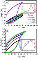
The structure, electric field-induced strain (EFIS), polarization and piezoelectric response of lead-free Sr3FeNb2O9-modified (Bi1/2Na1/2)0.935Ba0.065TiO3 (BNBT–xSFN, with x = 0–0.012) ceramics were investigated. XRD patterns show that all compositions have a pure perovskite structure and SFN effectively diffused into the BNBT lattice during sintering to form a solid solution. A large EFIS of 0.35% was obtained at the critical composition of x = 0.009 which corresponds to a normalized strain (Smax/Emax) of 583 pm V−1. A maximum value of piezoelectric constant (254 pC N−1) was obtained for x = 0.006. These results show our research can benefit the developments of Bi1/2Na1/2TiO3 ceramics and widen their range of applications.


1. Introduction

Lead-free electronic materials based on piezoceramics have experienced renewed interest in the last decade mainly motivated by the strict environmental regulations that are being enforced worldwide.1 Scientific research communities across the world have been looking for novel lead-free materials that have excellent piezoelectric and ferroelectric performance, which can be utilized widely in piezoelectric and ferroelectric applications. Lead-free systems with perovskite structure such as (K, Na)NbO3, BaTiO3, and (Bi1/2Na1/2)TiO3 (BNT)-based ceramics are found to be potential nontoxic candidates to replace the omnipresent lead based ceramics in such applications.2–7

Among them, BNT-based ceramics have been considered to be one of the most promising lead-free piezoelectric materials owing to their high ferroelectric responses (Pr = 38 μC cm−2) and high Curie temperature (320 °C). However, high conductivity and high coercive field (73 kV cm−1) can cause problems in the poling process, and thus limit its use in practical application.8,9 In order to improve the piezoelectric properties of BNT ceramics, various binary or ternary BNT-based solid solutions10–12 were proposed by adding new component such as BaTiO3,13 SrTiO3,14 Bi1/2K1/2TiO3,15 BaZrO3 (ref. 16) and K1/2Na1/2NbO3.17 Although many efforts have been devoted in further improving the electromechanical response and a few devices with acceptable performance were demonstrated, the global electrical properties of lead free counterparts were still inferior to the lead-based system. A large piezoelectricity is expected for sufficient performance in the BNT-based solid solutions with a composition near the morphotropic phase boundary (MPB) where the materials show superior piezoelectric properties. Recently, some investigations have concentrated on the perovskite modifications as new component to add the MPB composition of (1 − x)Bi1/2Na1/2TiO3-xBaTiO3 (BNBT) piezoceramics, which revealed enhanced properties with a piezoelectric constant (d33) of 146 pC N−1 at x = 0.065.13 Based on the MPB composition, BNBT has been further modified to trigger a large electric field-induced strain (EFIS) response via adding new component include Al6Bi2O12,18 K1/2Na1/2NbO3,19 BiAlO3 (ref. 20) and BaSrTiO3.21 Appropriate new component modifications are likely to influence the piezoelectric and EFIS properties of lead-free BNBT system. EFIS is one of the most important parameters for electromechanical actuators. BNT-based materials are expected to be superior lead-free candidates, as they exhibit giant electric field-induced strain response.10,19,22

Pham et al.23 studied a Nb-doped Bi0.5(Na0.82K0.18)0.5TiO3 system and reported a significant strain of 0.44% at 70 kV cm−1 with 3 mol% Nb. Sayyed et al.24 proposed the doping of SrTiO3 into BNT and observed coexistence of rhombohedral and pseudocubic with an enhancement in dielectric and piezoelectric properties. Li et al.25 prepared Fe-modified 0.875Bi0.5Na0.5TiO3–0.06Bi0.5Li0.5TiO3–0.065BaTiO3–0.005Mn ceramic near the morphotropic phase boundary (MPB) with a large unipolar strain of 0.4% obtained under 40 kV cm−1. Besides, Sr3FeNb2O9 (SFN) is a double-perovskite oxide with tetragonal crystal structure at room temperature. It also exhibits interesting structural, as well as desirable properties.26 Motivated by the above consideration, we hoped that the addition of SFN could enhance the piezoelectric and electric field-induced strain properties of the BNT-based ceramics. A new lead-free piezoelectric solid solution of (1 − x) (Bi1/2Na1/2)0.935Ba0.065TiO3x Sr3FeNb2O9 (BNBT–xSFN) with x varying from 0 to 0.012 was designed and then prepared by a conventional solid-state reaction method. The crystal structure and EFIS behaviors, piezoelectric, and ferroelectric properties have been systematically investigated to develop lead-free piezoelectric materials with large strain response for actuator application.

2. Experimental procedure

The BNBT–xSFN (x = 0–0.012) piezoelectric ceramics were synthesized by conventional solid-state reaction method using analytical-grade metal oxide or carbonate powders as starting materials. These powder mixtures were ball-milled for 12 h in ethanol with zirconia balls as milling media and then calcined at 850 °C for 2 h. Disk-shaped ceramic specimens of 12 mm diameter were prepared by compacting the calcined power. These were sintered at 1140 °C for 3 h in covered alumina crucibles. Structure and electrical characterizations are similar as that reported elsewhere.27

3. Results and discussion

Fig. 1(a) plots the X-ray diffraction (XRD) patterns of the ceramics measured in 2θ = 20–70°. All the ceramics have a pure perovskite phase, showing that a stable solution exists even if the SFN is in the range of 0–0.012. Expanded XRD patterns in 2θ range of ∼45–48.5° revealed that all BNBT–xSFN composition exhibited typical characteristics of tetragonal symmetry evident by the splitting of (002)/(200) peaks at 2θ of near 46.5, as shown in Fig. 1(b). In addition, the overall effect of SFN substitution on the XRD patterns of the BNBT ceramics is the slight shift of intensity peaks towards higher angles, suggesting the shrinkage of lattice constant.28,29 Similar peak shifts were also reported in CaTiO3-doped BNT ceramics and CuO modified BNKT ceramics.30,31
image file: c5ra17781b-f1.tif
Fig. 1 XRD patterns of BNBT–xSFN ceramics in the 2θ range: (a) 20–70° and (b) 45–48.5°.

Fig. 2 shows SEM micrographs of various SFN doped BNBT ceramics. The SEM observation confirms that all the investigated samples are visibly dense. The loose microstructure with the blur grain boundaries is observed in Fig. 2(b) and (d). The evaporation of bismuth and sodium metal elements which can lead to titanium excess might be the most important reason for poor sintering. Moreover, these micrographs also indicated that SFN-doped causes a significant change in grain shape and size: the average grain size first increased and then decreased with increasing SFN contents. The accelerated grain growth associated with a small amount of SFN additive may result from an emergence of oxygen vacancies, which are favorable for the transport of mass in the sintering process, and also strongly promotes grain growth.32,33 However, excess SFN doping restrain grain growth, excess SFN can concentrate near grain boundaries and decrease their mobility substantially. Thus, the mass transportation is weakened and grain growth is inhibited.34 To ensure the accuracy of the results, the sample is used for the EDS analysis. As shown in Fig. 3, the SFN elements were detected both in grain regions and grain boundary regions. Therefore, it was concluded that excess SFN inhibited the grain growth of BNBT–xSFN ceramics.


image file: c5ra17781b-f2.tif
Fig. 2 SEM micrographs of surfaces for BNBT–xSFN ceramics sintered at 1140 °C: (a) x = 0, (b) x = 0.003, (c) x = 0.009, (d) x = 0.012.

image file: c5ra17781b-f3.tif
Fig. 3 EDS spectra of spot analysis of BNBT–xSFN ceramics in grain regions and grain boundary regions: (a) grain regions and (b) grain boundary regions.

Electric-field-induced polarization (PE) hysteresis and strain (SE) loops were displayed in Fig. 4(a) and (b), respectively. Well-saturated hysteresis loops of unmodified BNBT–xSFN (x = 0) show a relatively large remnant polarization (Pr) and coercive field (Ec), with typical butterfly-shaped SE curves having a clearly visible negative strain. With SFN increasing, the long-range ferroelectric order is significantly disrupted, the “pinching” of the PE loops indicating the development of a relaxor ferroelectric phase at zero field. This compositionally induced ferroelectric to relaxor ferroelectric phase transformation is also verified by SE loop measurements. In the SE loops of x = 0.009 ceramic shown in Fig. 4(b), the negative strain can be seen to almost vanish, resulting in the largest strain observed in this system when the ferroelectric and relaxor ferroelectric phases seem to exist simultaneously.35–37 Therefore, it seems that a reversible relaxor ferroelectric–ferroelectric phase transition occurs in response to an applied electric field.


image file: c5ra17781b-f4.tif
Fig. 4 Effects of SFN doping on the ferroelectric and field-induced strain properties of BNBT–xSFN ceramics; (a) PE loops and (b) bipolar SE loops.

The composition dependence of the polarization hysteresis loops was investigated at room temperature and the corresponding polarization current curves were simultaneously collected as they are known to be more sensitive to polarization state, as shown in Fig. 5. The samples of x = 0 and x = 0.003 exhibited a typical rectangular loop with the remnant polarization (Pr) of 26.3 μC cm−2, 38.2 μC cm−2 and the coercive field (Ec) of 38.9 kV cm−1, 30.7 kV cm−1, respectively. One sharp polarization current peak (denoted as P1) ascribed to the ferroelectric domains switching could be observed when the applied field reached Ec. With x increased to x = 0.006, slightly pinched PE loop appeared along with an additional current peaks (denoted as P2). The Ec corresponding to P1 shifted to lower electric field direction. The aligned macroscopic ferroelectric domains turned into randomly oriented ferroelectric domains, as the electric field increased from 0 to Ec. Then the randomly oriented polar nanoregions (PNRs) were stimulated with the further increased driving field and aligned to form field-induced long-range order ferroelectric domains.38 When x further increased to 0.009, the obvious pinched behavior appeared, implying that the dominant ferroelectric order in BNBT was disturbed with the addition of SFN. The randomly oriented macroscopic ferroelectric domains could be decomposed by only a relatively small voltage due to the “weak” ferroelectric phase. This process produced a small current peak which was not obvious. With the increase of electric field, the randomly oriented PNRs aligned under the external field and form field-induced long-range order ferroelectric domains. In order to decompose the increased ferroelectric domains, an obvious current peak occurs when the current decrease.39


image file: c5ra17781b-f5.tif
Fig. 5 Room-temperature ferroelectric loops and polarization current curves of (a) x = 0, (b) x = 0.003, (c) x = 0.006, (d) x = 0.009, and (e) x = 0.012.

A clear relation between domains and morphology and dielectric frequency dispersion has been established, nanodomains correspond to strong frequency dispersion while large domains show weaker frequency dependence.40 Therefore, the domains evolution can be characterized by the dielectric spectrum. The temperature dependence of dielectric constant (εr) and loss (tan[thin space (1/6-em)]δ) for all samples from room temperature to 500 °C in the range 1 kHz to 100 kHz are shown in Fig. 6. It is observed that a clear change for x ≤ 0.006 samples at low temperature region with a relatively weak frequency-dependent dispersion and decreasing dielectric constant. It is suggested that BNBT–xSFN ceramics with x ≤ 0.006 are nonergodic relaxor ferroelectrics state undergoing a field-induced phase transition to a long-range ordered state.41 This means that the initially PNRs are triggered to grow into micron-sized domains or ordered reorientation with the application of electric field. It is also interesting to note that the frequency-dependent dispersion and dielectric constant for the specimens with x ≥ 0.009 show only slight variation. This indicates that the BNBT–xSFN ceramics with x ≥ 0.009 are ergodic relaxor ferroelectrics.


image file: c5ra17781b-f6.tif
Fig. 6 Temperature dependence of the dielectric constant and loss of BNBT–xSFN ceramics at various frequencies.

EFIS response of piezoelectric ceramics is considered to be an important property of the materials used in actuator applications. The composition dependent field-induced unipolar strain curves in Fig. 7(a) show a similar trend to the bipolar strain. The EFIS level significantly increased with increasing x = 0 up to x = 0.009 and then it drops drastically. The EFIS response for x < 0.009 is almost linear at 60 kV cm−1, however, a highest strain of 0.35% and a corresponding Smax/Emax of 583 pm V−1 are attained at x = 0.009 with an applied electric field of 60 kV cm−1. The origin of this large strain could be attributed to the coexistence of ferroelectric and relaxor ferroelectric orders which possess competitive free energies (evident from bipolar strain and PE loop results).


image file: c5ra17781b-f7.tif
Fig. 7 (a) Unipolar strain curves of the BNBT–xSFN ceramics and (b) unipolar strain curves of BNBT–xSFN ceramics with x = 0.009 as a function of the applied field.

To evaluate the optimized EFIS response of the BNBT–0.009SFN ceramics, it was examined under different electric fields. A large EFIS of 0.35% was perceived at a low applied field of 60 kV cm−1 which corresponds to Smax/Emax of 583 pm V−1. Even at low applied field of 45 kV cm−1, BNBT–0.009SFN displayed a high strain of 0.206% corresponding to Smax/Emax of 457 pm V−1 which is higher than other BNT-based ceramics, as shown in Fig. 7(b). Most of the BNT-based systems required a high driving field in order to achieve a high EFIS.12,42,43 This large EFIS at low applied field indicates that the BNBT–0.009SFN system is a potential candidate material for environmentally friendly electromechanical devices and actuator applications.

Fig. 8 shows piezoelectric constant (d33) of the BNBT–xSFN ceramics sintered at 1140 °C. From Fig. 8, with x increasing, the piezoelectric constant (d33) increase firstly and reaches peak values of d33 = 254 pC N−1 at x = 0.006, and then rapidly drop as the x further increase. To our best knowledge, large d33 value in x = 0.006 sample is considerably higher than other previously reported results in the BNT-based ceramics,44–46 indicating that the ceramics used in this work are promising candidates for piezoelectric devices.


image file: c5ra17781b-f8.tif
Fig. 8 Piezoelectric constant (d33) of the BNBT–xSFN ceramics as a function of x.

4. Conclusions

The effects of SFN substitution on BNBT ceramics was investigated in terms of crystal structure, field-induced strain, ferroelectric and piezoelectric properties to explore good lead-free materials for practical applications. Encouraging results of field-induced unipolar strain (0.35%) corresponding to a normalized strain (Smax/Emax = 583 pm V−1) and piezoelectric constant (d33 = 254 pC N−1) are realized at room temperature for BNBT–xSFN ceramics. It is obvious that this piezoceramic is promising candidate for lead-free piezoceramic and can be used in practical applications.

Acknowledgements

This work was supported by the National Natural Science Foundation of China (No. 51372110, 51402144, 51302124, 51302025, 51502127), National High Technology Research and Development Program of China (No. 2013AA030801), Science and Technology Planning Project of Guangdong Province, China (No. 2013B091000001), Independent innovation and achievement transformation in Shandong Province special, China (No. 2014CGZH0904), The Project of Shandong Province Higher Educational Science and Technology Program (No. J14LA11, No. J14LA10).

References

  1. J. Rödel, W. Jo, K. T. Seifert, E. M. Anton, T. Granzow and D. Damjanovic, J. Am. Ceram. Soc., 2009, 92, 1153–1177 CrossRef PubMed.
  2. Y. Saito, H. Takao, T. Tani, T. Nonoyama, K. Takatori, T. Homma, T. Nagaya and M. Nakamura, Nature, 2004, 432, 84–87 CrossRef CAS PubMed.
  3. E. Cross, Nature, 2004, 432, 24–25 CrossRef CAS PubMed.
  4. E. Hollenstein, M. Davis, D. Damjanovic and N. Setter, Appl. Phys. Lett., 2005, 87, 182905 CrossRef PubMed.
  5. N. Ma, B. P. Zhang, W.-G. Yang and D. Guo, J. Eur. Ceram. Soc., 2012, 32, 1059–1066 CrossRef CAS PubMed.
  6. X. Wang, X. Tang and H. Chan, Appl. Phys. Lett., 2014, 85, 91 CrossRef PubMed.
  7. R. Cheng, Z. Xu, R. Chu, J. Hao, J. Du and G. Li, J. Alloys Compd., 2015, 632, 580 CrossRef CAS PubMed.
  8. K. Sakata and Y. Masuda, Ferroelectrics, 1974, 7, 347–349 CrossRef CAS PubMed.
  9. Y. Hiruma, H. Nagata and T. Takenaka, J. Appl. Phys., 2008, 104, 4106 CrossRef PubMed.
  10. Y. Hiruma, H. Nagata and T. Takenaka, Appl. Phys. Lett., 2009, 95, 2903 CrossRef PubMed.
  11. Y. Li, F. Wang, X. Ye, Y. Xie, Y. Tang, D. Sun, W. Shi, X. Zhao, H. Luo and W. Jo, J. Am. Ceram. Soc., 2014, 97, 3615–3623 CrossRef CAS PubMed.
  12. J. Hao, B. Shen, J. Zhai, H. Chen and S. Zhang, J. Am. Ceram. Soc., 2014, 97, 1776–1784 CrossRef CAS PubMed.
  13. Y. S. Sung, J. M. Kim, J. H. Cho, T. K. Song, M. H. Kim and T. G. Park, Appl. Phys. Lett., 2010, 96, 2901 Search PubMed.
  14. W. Krauss, D. Schütz, F. A. Mautner, A. Feteira and K. Reichmann, J. Eur. Ceram. Soc., 2010, 30, 1827–1832 CrossRef CAS PubMed.
  15. K. Yoshii, Y. Hiruma, H. Nagata and T. Takenaka, Jpn. J. Appl. Phys., 2006, 45, 4493–4496 CrossRef CAS.
  16. J. U. Rahman, A. Hussain, A. Maqbool, T. K. Song, W. J. Kim, S. S. Kim and M. H. Kim, Curr. Appl. Phys., 2014, 14, 331–336 CrossRef PubMed.
  17. A. B. Kounga, S. T. Zhang, W. Jo, T. Granzow and J. Rodel, Appl. Phys. Lett., 2008, 92, 222902–222903 CrossRef PubMed.
  18. R. Cheng, Z. Xu, R. Chu, J. Hao, J. Du and G. Li, RSC Adv., 2015, 5, 41646–41652 RSC.
  19. S. T. Zhang, A. B. Kounga, E. Aulbach, H. Ehrenberg and J. Rödel, Appl. Phys. Lett., 2007, 91, 112906 CrossRef PubMed.
  20. D. S. Lee, D. H Lim, M. S Kim, H. K Kwang and J. J Soon, Appl. Phys. Lett., 2011, 99, 062906 CrossRef PubMed.
  21. J. Shi, H. Fan, X. Liu, Y. Ma and Q. Li, J. Alloys Compd., 2015, 627, 463–467 CrossRef CAS PubMed.
  22. W. Liu and X. Ren, Phys. Rev. Lett., 2009, 103, 257602 CrossRef.
  23. K. N. Pham, A. Hussain, C. W. Ahn, I. W. Kim, S. J. Jeong and J. S. Lee, Mater. Lett., 2010, 64, 2219–2222 CrossRef CAS PubMed.
  24. S. Sayyed, S. A Acharya, P. Kautkar and V. Sathe, RSC Adv., 2015, 5, 50644–50654 RSC.
  25. J. Li, F. Wang and C. M. Leung, et al., J. Mater. Sci., 2011, 46, 5702–5708 CrossRef CAS.
  26. Y. Cha, J. Bae, T. Hong, J. Yoon, E. Chung, E. Jeong, H. Kim, P. Borse and K. Lim, J. Korean Phys. Soc., 2014, 65, 520–525 CrossRef CAS.
  27. R. Cheng, Z. Xu, R. Chu, J. Hao, J. Du, W. Ji and G. Li, Ceram. Int., 2015, 41, 8119–8127 CrossRef CAS PubMed.
  28. Y. Sung, J. Kim, J. Cho, T. Song, M. Kim and T. Park, Appl. Phys. Lett., 2010, 96, 2901 Search PubMed.
  29. Y. Hiruma, Y. Imai, Y. Watanabe, H. Nagata and T. Takenaka, Appl. Phys. Lett., 2008, 92, 2904 CrossRef PubMed.
  30. Y. Yuan, E. Li, B. Li, B. Tang and X. Zhou, J. Electron. Mater., 2011, 40, 2234–2239 CrossRef CAS.
  31. J. K. Kang, D. J. Heo, V. Q. Nguyen, H. S. Han, J. S. Lee and K. K. Ahn, J. Korean Phys. Soc., 2012, 61, 899–902 CrossRef CAS.
  32. Y. Guo, H. Fan, C. Long, J. Shi, L. Yang and S. Lei, J. Alloys Compd., 2014, 610, 189–195 CrossRef CAS PubMed.
  33. M. Zhu, L. Liu, Y. Hou, H. Wang and H. Yan, J. Am. Ceram. Soc., 2007, 90, 120–124 CrossRef CAS PubMed.
  34. V. Pal, R. K. Dwivedi and O. P. Thakur, Mater. Res. Bull., 2014, 51, 189–196 CrossRef CAS PubMed.
  35. J. Hao, B. Shen, J. Zhai and H. Chen, J. Appl. Phys., 2014, 115, 034101 CrossRef PubMed.
  36. K. Wang, A. Hussain, W. Jo and J. R. R. Del, J. Am. Ceram. Soc., 2012, 95, 2241–2247 CrossRef CAS PubMed.
  37. A. Hussain, J. U. Rahman, A. Zaman, R. A. Malik, J. S. Kim, T. K. Song, W. J. Kim and M. H. Kim, Mater. Chem. Phys., 2014, 143, 1282–1288 CrossRef CAS PubMed.
  38. R. Dittmer, D. Gobeljic, W. Jo, V. V. Shvartsman, D. C. Lupascu, J. L. Jones and J. Rodel, J. Appl. Phys., 2014, 115, 084111 CrossRef PubMed.
  39. Y. Guo, H. Fan and J. Shi, J. Mater. Sci., 2015, 50, 403–411 CrossRef CAS.
  40. C. Ma, X. Tan, E. Dul'kin and M. Roth, J. Appl. Phys., 2010, 108, 104105 CrossRef PubMed.
  41. R. Garg, B. N. Rao, A. Senyshyn, P. S. R. Krishna and R. Ranjan, Phys. Rev. B: Condens. Matter Mater. Phys., 2013, 88, 014103 CrossRef.
  42. J. Hao, B. Shen and J. Zhai, et al., J. Appl. Phys., 2014, 115, 034101 CrossRef PubMed.
  43. J. U. Rahman, A. Hussain and A. Maqbool, J. Alloys Compd., 2014, 593, 97–102 CrossRef CAS PubMed.
  44. A. Ullah, C. W. Ahn and R. A. Malik, J. Electroceram., 2014, 33, 187–194 CrossRef CAS.
  45. W. L. Li, W. P Cao and D. Xu, J. Alloys Compd., 2014, 613, 181–186 CrossRef CAS PubMed.
  46. Q. Yao, F. Wang and F. Xu, ACS Appl. Mater. Interfaces, 2015, 7, 5066–5075 CAS.

This journal is © The Royal Society of Chemistry 2015
Click here to see how this site uses Cookies. View our privacy policy here.