
 Open Access Article
 This Open Access Article is licensed under a
 Creative Commons Attribution 3.0 Unported Licence
Large-area scanning probe nanolithography facilitated by automated alignment of probe arrays
Shuai Wang†
a,
Joseph Hosford†b,
William P. Heath*a and
Lu Shin Wong*b
aSchool of Electrical and Electronic Engineering, University of Manchester, Manchester M13 9PL, UK. E-mail: william.heath@manchester.ac.uk; Tel: +44 (0)161 3064659
bManchester Institute of Biotechnology & School of Chemistry, University of Manchester, Manchester M1 7DN, UK. E-mail: l.s.wong@manchester.ac.uk; Tel: +44 (0)161 3068939
First published on 26th June 2015
Abstract
The precision and versatility afforded by scanning probe microscopy has enabled the development of a variety of methods for the facile fabrication of user-defined patterns on a variety of surfaces with nanoscale resolution. Historically, the major limitation of such scanning-probe nanolithography has been the inherently low throughput of single probe instrumentation, which has been addressed by the use of “two-dimensional” arrays of multiple probes for parallelised nanolithography. Key to the successful implementation of such arrays is a means to accurately align them relative to the substrate surface, such that all probes come into contact with the surface simultaneously upon the commencement of lithography. Here, an algorithm for the rapid, accurate and automated alignment of an array is described in the context of polymer pen lithography. This automation enables the alignment of the array of probes within minutes, without user intervention. Subsequent nanolithography of thiols on gold substrates demonstrated the generation of features over large (cm2) areas with high uniformity. Example features were 66.5 ± 9.8 and 71.3 ± 9.3 nm in size across a distance of 1.4 cm, indicating any misalignment as ≤0.0003°.
Introduction
A critical requirement in the development of device nanofabrication for sensing, diagnostics and computing is the need to generate nanometre-sized features on surface substrates.1–3 In this regard, the application of scanning probe methods for lithography such as those derived from atomic force microscopy (AFM) have been a long-standing area of research.4–7 Such scanning probe lithography (SPL) methods are of particular interest since the piezo-electrically actuated probes can be used to conveniently and rapidly “write” any arbitrary user-defined pattern. In comparison with conventional nanofabrication methods derived from the microelectronics sector, the capabilities of SPL are particularly useful for the rapid development and prototyping of new structures and devices since SPL can be accessed at relatively low cost without the need for specialised laboratory facilities. In its simplest form, SPL can be achieved by mechanical displacement of materials (‘nanoshaving’ or ‘nanoscratching’), or with subsequent back-filling using a different material (nanografting).4,6 Physical methods such as an application of an electrical bias across the probe and surface to generate patterns of oxidised material (local anodic oxidation),8 local heating (thermochemical nanolithography)9 and probe-directed photolithography (scanning near-field photolithography)10 have also been reported. Another important approach to SPL is to use the probes as a “pen” to deposit materials on to a surface, through the use of probes coated with the molecules to be deposited (dip-pen nanolithography, DPN),11 or through the use of probes engineered with channels for fluid delivery (nanopipettes and nano-fountain pens).12–14Historically, the major limitation of SPL was that writing with a single probe is a serial process, and was therefore inherently low throughput.15 To address this issue, many researchers have developed parallelised systems that instead utilise arrays of multiple probes. Initial efforts resulted in “one-dimensional” arrays with a single row of probes,16–19 but the pursuit of ever increasing lithography throughput rapidly led to the production of “two-dimensional” arrays of probes that now allow the lithography of cm2 areas while maintaining submicron resolution.20–24 The first examples of two-dimensional probe arrays that were developed were cantilevered arrays. However, since these arrays were fabricated using conventional microfabrication technology they were complex to produce, expensive and fragile. These considerations led to the development of cantilever-free approaches such as polymer pen lithography (PPL),22,25 beam pen lithography (BPL)24 and hard-tip soft-spring lithography (HSL),23 which utilised soft elastomeric materials in order to produce the probe arrays.
A key requirement for the implementation of this technology is that the array must be fully aligned parallel to the surface so that all probes come into contact with the surface simultaneously upon writing (Fig. 1A). Any misalignment results in the individual probes coming into contact with the surface at different distances. This issue is particularly critical when PPL arrays are used, since their resolution is dependent on the amount of contact (and therefore the amount of force exerted on to the probes upon contact) between the probes and the surface (Fig. 1B). Due to the extreme resolution required, the tolerance for misalignment over the length of the array is small – even 0.01° deviation away from the parallel across a 1 cm2 probe array results in a ∼50% difference in feature size from one side of the array to the other (Fig. 1C).26
 | ||
| Fig. 1 Schematic diagrams of a PPL probe array's approach to the surface. (A) The ideal situation of a fully aligned array, where all probes in the array come into contact simultaneously as the array approaches the surface. (B) The approach of misaligned probes results in non-uniform lithography across the surface. (C) Example optical microscopy images of gold features at opposite ends of a dot array approximately 1 cm apart. The features were formed after etching of a gold-coated substrate that was patterned by PPL deposition of 16-mercaptohexadecanoic acid, using an array that was misaligned by approximately 0.01°. | ||
In early reports, the alignment process prior to printing was primarily achieved through visual inspection of the probe array as it was brought into contact with the surface.22,27 In this method, the instrument operator observes a live image of the probes and as they are brought into contact, a deformation of the pyramidal probes (if elastomeric) or a deflection of the probe cantilevers (if stiff probes) can be observed. The operator notes which side of the array first comes into contact and then adjusts the tilt of the sample stage to compensate. This process of observing the probe approach and adjustment is then repeated until alignment is achieved. This optimisation of the tilt angle must be repeated for both x- and y-axes to ensure all the probes in a two-dimensional array are aligned. Since this method relies on the operator to observe and manually adjust the angle of the sample relative to the array, the reproducibility and accuracy of the alignment process is relatively poor, typically >0.02°.26
In order to address the subjectivity of visual observations by the operator, a method that utilises the amount of force exerted by the contact of the probes on to the surface has been reported.26 Here, it was noted that the amount of force exerted by the probes on to the surface was dependent on the distance travelled as the probes advanced towards the surface. As the distance is reduced, initially no force is registered until contact is achieved, after which the force continues to increase with reducing distance as the probes are pushed on to the surface. Additionally, the amount of force exerted also depends on the amount of (mis)alignment of the array. If the array is fully aligned, all probes will come into contact with the surface simultaneously and a maximal downward force would be exerted for a given distance travelled below the point of contact. If the array is misaligned, fewer probes will be in contact, and the force exerted will be reduced. Thus, instead of using subjective visual observations, the operator could align the probe array in the iterative approach-observe-withdraw-adjust process using the force measurements. Using this approach, alignment to within 0.004° was demonstrated. In practical terms, this “force feedback” strategy is readily implemented by simply installing a force sensor at the base of the sample stage of an existing AFM.
The current limitation of SPL is therefore the need to undertake this iterative process, which is time-consuming and extremely tedious for the operator. Indeed, the alignment process is often several-fold longer (2–4 hours) than the actual lithography process (usually <1 hour). Implementation of an algorithm that automates this task would therefore greatly enhance the usability of SPL technology.
Herein, the development of a modified AFM system is reported that enables large-area SPL. The system employs the detection of force using multiple force sensors as the means of determining probe-surface contact, together with an algorithm that automates the iterative alignment process.
Results and discussion
In terms of the hardware, this study employed an AFM that is able to scan the probes across three axes (x, y and z). This AFM is placed above a custom-built translating stage which itself is capable of movement with five degrees of freedom, i.e. across the three axes as well as tilting in two axes θ and φ. Three load cell force sensors are placed beneath the sample stage (Fig. 2).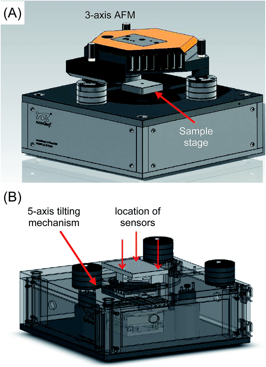 | ||
| Fig. 2 Schematic diagrams of the SPL instrument. (A) Assembled components showing the AFM and sample stage. (B) Detail of tilting sample stage illustrating the location of the sensors under the sample stage. | ||
Probe array alignment algorithm
In principle, the algorithm automates the tasks that would have been undertaken by a human operator when performing the alignment procedure: to advance the probes towards the surface, record the distance travelled in order to exert a pre-determined amount of force on the sensors; then retract the probes and adjust the tilt by a pre-set amount. Here, the force measurement used is the sum of all three sensors and the threshold at which contact is registered by the algorithm is typically set to 490 μN. This value was chosen as it was found to reliably give an unambiguous indication of probe contact above the background noise, which was found to have a baseline value of ∼49 μN but with occasional spikes of up to 250 μN. By iterating this process across a range of tilt angles, the relationship between the point on the z-axis (the “z-position”) at which the probes exert the required force, and the tilt angle of the stage is recorded. The tilt angle that requires the greatest extension of the probes in the z-axis before coming into contact with the surface would be expected to correspond to the angle that achieves fully parallel alignment. This process is then repeated for the second tilt axis in order to complete the alignment of a two-dimensional array of probes.An illustrative example of the relationships between the tilt angle (θ or φ) and the z-position recorded is shown in Fig. 3. At the start of the process (henceforth referred to as Step 1), since the probe array is not aligned on either tilt axis, for an arbitrarily fixed φ it is observed that the z-position varies as the angle θ is varied (Fig. 3A). These z-positions can be divided into two regimes, a rising trend up to a maximum followed by a subsequent fall at approximately the same rate. This data can be fitted to two lines in order to determine their intersection, which is the point where θ gives the maximum z extension. This point, termed θoptimum1, is therefore the angle at which the stage must be tilted in order to achieve parallel alignment along this axis for the given φ.
 | ||
Fig. 3 Graphs illustrating the relationships between the tilt angles and z position, where  indicates the actual values measured and indicates the actual values measured and  indicates the best fit with the least-squares method. (A) In Step 1, a series of z-positions is obtained over a range of θ values. The maximum z-position is obtained by calculating the intersection between the two linear best fits for the rising and dropping arms, which corresponds to θoptimum1. (B) In Step 2, φoptimum1 is determined in a similar way by varying φ and measuring the z-position, where the θ angle used is fixed as the θoptimum1 + 150 m°. Steps 3 and 4 are treated in a similar manner. indicates the best fit with the least-squares method. (A) In Step 1, a series of z-positions is obtained over a range of θ values. The maximum z-position is obtained by calculating the intersection between the two linear best fits for the rising and dropping arms, which corresponds to θoptimum1. (B) In Step 2, φoptimum1 is determined in a similar way by varying φ and measuring the z-position, where the θ angle used is fixed as the θoptimum1 + 150 m°. Steps 3 and 4 are treated in a similar manner. | ||
However, once this first optimum θ angle is reached it was found that the change in the z-position as a function of φ becomes extremely small and very sensitive to any probe inhomogeneity on the probe array. As a result, accurate determination of this optimum becomes difficult. Instead, after determining the optimum in one axis, the array is deliberately tilted by 150 m° away from the optimum before the alignment of the other axis is performed. Thus in Step 2, the angle θ is fixed as θoptimum1 + 150 m° and φ is varied to obtain another series of z-positions (Fig. 3B). In a similar way to Step 1, φoptimum1 corresponding to the maximum z-position is calculated. In Step 3, θ is again varied but now using φ fixed at φoptimum1 − 150 m°, which results in the generation of another optimal θ value, θoptimum2. Step 4 then uses θoptimum2 − 150 m° to determine φoptimum2. The four (θ, φ) pairs from each of the steps are then represented in a coordinate system (Fig. 4). Using these coordinates, the fully optimised (θ, φ) pair that is appropriated from the intersection of the four experimentally determined pairs correlates to the final overall optimal tilt angles.
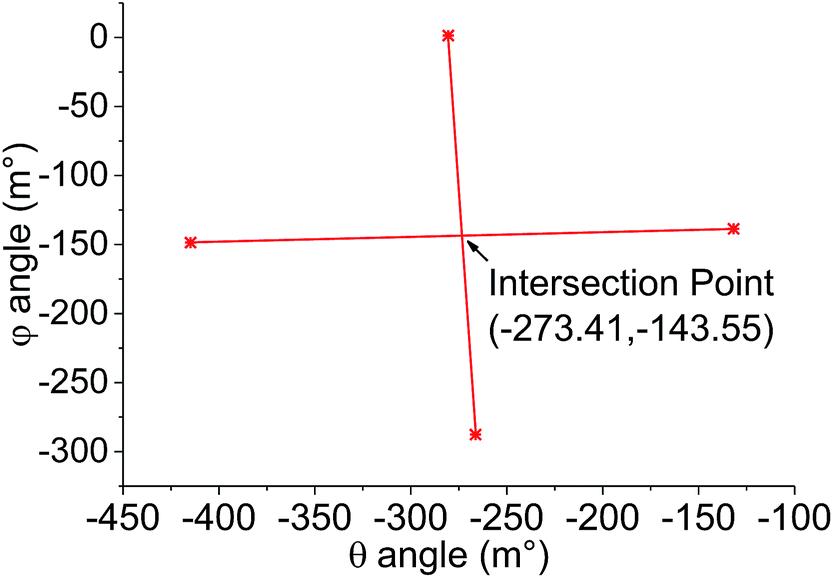 | ||
| Fig. 4 Graph of φ against θ with the plots of the four points where the maximum z-position was reached. The middle point marked in red is calculated as the final overall optimum tilt angle across both axes. | ||
Additionally, it was found that by incorporating three sensors within the sample stage, it was possible to determine which part of the array first comes into contact with the surface during approach. Since the probe array is centred relative to the sensors, in addition to simply registering the maximum total force upon contact, when full alignment is achieved all force sensors also registered an equal amount of force on each sensor (196 μN each in this case). Thus, multiple sensors also allow a second check on the alignment of the probe array after the alignment procedure.
Large-area nanolithography
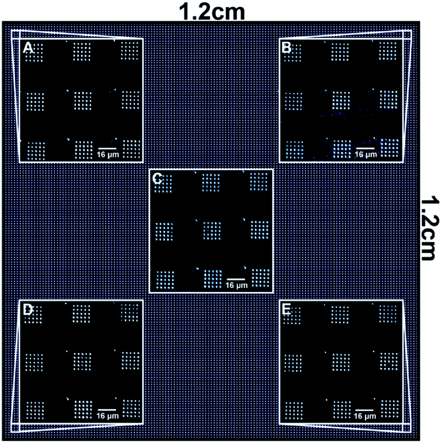
To validate the performance of the alignment algorithm, PPL was undertaken by depositing 16-mercaptohexadecanoic acid on to a gold substrate as a model system. Here, a 1.2 × 1.2 cm2 PPL array with 100 μm pen pitch and 28 μm pen height was used for the nanolithography. In order to make it possible to locate the deposited patterns during subsequent imaging over a large area, a template consisting of a 5 × 5 array of microscale oval features (Fig. 5A and B) was used, which were themselves constituted from a series of smaller nanoscale oval features (Fig. 5C). AFM imaging of printed areas located as far apart as 1.4 cm indicated that the feature sizes were uniform throughout (Fig. 6). In both cases, the measured mean diameter (full width at half maximum height, FWHM) of the nanoscale oval features, such as those shown in Fig. 5C at the diagonal locations, were 66.5 ± 9.8 nm (lower left) and 71.3 ± 9.3 nm (top right). These results were within the experimental error and maximum practical resolution of the PPL method,22 thus indicating any misalignment was less than the minimum tilt step that can be achieved by this hardware configuration, ≤0.3 m°.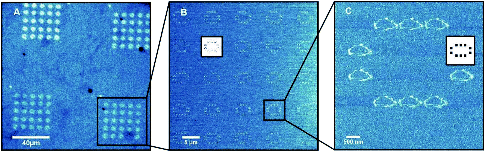 | ||
| Fig. 5 Images showing sequential magnifications of the pattern produced by PPL deposition of MHA on to gold: (A) an optical microscope image taken after 4 minutes exposure to gold enchant; (B and C) lateral force AFM images of the MHA deposited on to the gold with schematic inlays of the pixel pattern used. | ||
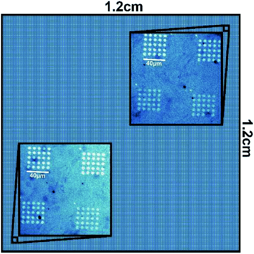 | ||
| Fig. 6 Diagram illustrating locations imaged by AFM for size measurements with the insets showing the microscopy images. | ||
In this model pattern, each probe performed the nanolithography of 2500 individual dot features, taking a total of 55 min for the entire write cycle. In comparison, the alignment process took an average of 35 min, thus demonstrating that the rate limiting step of this type of two-dimensional SPL is now due to the actual lithography process rather than the previously time-consuming and subjective alignment of the probe arrays.
Since the deposited 16-mercaptohexadecanoic acid can act as an etch resist, subsequent etching of the gold film results in the generation of gold features corresponding to the patterned template. To demonstrate the generation of these metallic features on the underlying glass substrate, each probe was used to produce a 5 × 5 array of 2 μm dot features, which were then etched and imaged by AFM. Images from five representative locations on the 1.2 × 1.2 cm2 printed area (Fig. 7) were further analysed (Table 1). This data showed good consistency throughout the printed area with the variation in feature size similar to that reported for the nanoscale features in Fig. 5.
 | ||
| Fig. 7 Diagram illustrating images of gold features on glass generated by the etching of the gold film after PPL. | ||
The gold features on the glass substrate also gave high optical contrast and were readily imaged by bright field optical microscopy, which provided a wider field of view. As a demonstration, a range of other patterns that were generated by PPL after using the reported alignment procedure were etched and imaged (Fig. 8). In all cases, these images show that the features were highly uniform throughout the printed area.
 | ||
| Fig. 8 Optical microscopy images of gold substrates that were patterned by the aligned PPL arrays and subsequently etched. | ||
In this hardware configuration the PPL array is attached on a magnetic kinematic mount, which enables the array to be reproducibly repositioned if removed. Thus, it is possible to remove the array to add the “ink” between the alignment and lithography processes. In this manner, even viscous liquids may be employed without affecting the alignment procedure, and the alignment can be conducted without the unwanted deposition of any materials prior to lithography (Fig. 8B).
Conclusions
In summary, an SPL system that is capable of rapid, accurate and operator-free alignment of large two-dimensional arrays of scanning probes has been developed. Central to its operation is a tilt alignment optimisation algorithm that uses multiple force measurements from the sample stage. When used to perform PPL, this nanolithography platform is able to generate nanoscale features over large (cm2) areas with extremely high uniformity.This automation routine addresses what was previously a major limitation of multiprobe SPL since the alignment process was the most time-consuming and inaccurate step of such large-area parallelised nanolithography techniques. Indeed, this automated alignment now firmly places the rate-limiting step of the write cycle with the nanolithography operation itself. Although we have demonstrated the application of this alignment process to PPL, this algorithm is applicable to any other SPL that employs arrays of probes for material deposition including lipid-DPN28 and matrix-assisted methods,29 as well as possible future systems that could employ catalytic probes.30 As such, it will be applicable to any future development of scanning probe-based universal “desk-top fab” systems, and opens the possibility for the larger scale application of SPL in manufacturing.31,32
It should also be noted that the algorithm can be applied to any process that requires the alignment of two planes upon contact and is fully scalable to larger arrays or areas by placing the force sensors further apart. It could therefore be applied to a range of other areas manufacturing processes including stamping, printing or embossing.
Materials and methods
Materials and instrumentation
The AFM used was a FlexAFM with a C3000 controller (Nanosurf, Liestal, Switzerland) and has a nominal translation range of 100 μm in x and y axes and 11 μm in the z axis. The probe arrays were mounted on a custom made array holder in place of a conventional cantilever chip holder. The AFM was placed above a custom built (by Nanosurf) five-axis translation stage with a maximum x, y and z traverse of 72 mm, 46 mm and 5 mm, respectively; and a step resolution of 0.3 μm, 0.3 μm and 0.1 μm, respectively. The stage is able to tilt in both θ and φ axes across 10° with a maximum resolution of 0.3 m°. Incorporated into the sample stage are three metal foil strain gauge load cell sensors (FUTEK, Irvine, CA, USA), each with a sensitivity of 2 μN. The software code was written in LabVIEW V13.0 (32 bit). A user interface is built up to allow the operator to define as inputs the coarse and fine step lengths, angle step, and the path for data storage. The outputs are given by a real-time amplitude figure and an Excel file containing the results of all the force and positional data gathered during the alignment procedure. In order to incorporate the force measurements into the routine above, the USB DLL (Dynamic Linking Library) supplied by FUTEK is used for the LabVIEW software to acquire the data input from the sensors. The output from the software algorithm is used to control the z, θ and φ of the sample stage through an existing DLL for the Simple Control Unit (SCU) product family (USB version).AFM lateral force imaging was performed on the same instrument using ContAl-G cantilevers (Budget Sensors, Bulgaria) under ambient conditions.
The PPL arrays were prepared according to previously reported procedures.22 The gold substrates upon which the nanolithography was performed were purchased from Sigma Aldrich (2 nm titanium adhesion layer, 10 nm gold on aluminasilicate glass microscope slide). 16-Mercaptohexadecanoic acid, thiourea, iron(III) nitrate nonahydrate and hydrochloric acid (37%) were also purchased from Sigma Aldrich and used as received.
Probe array alignment algorithm
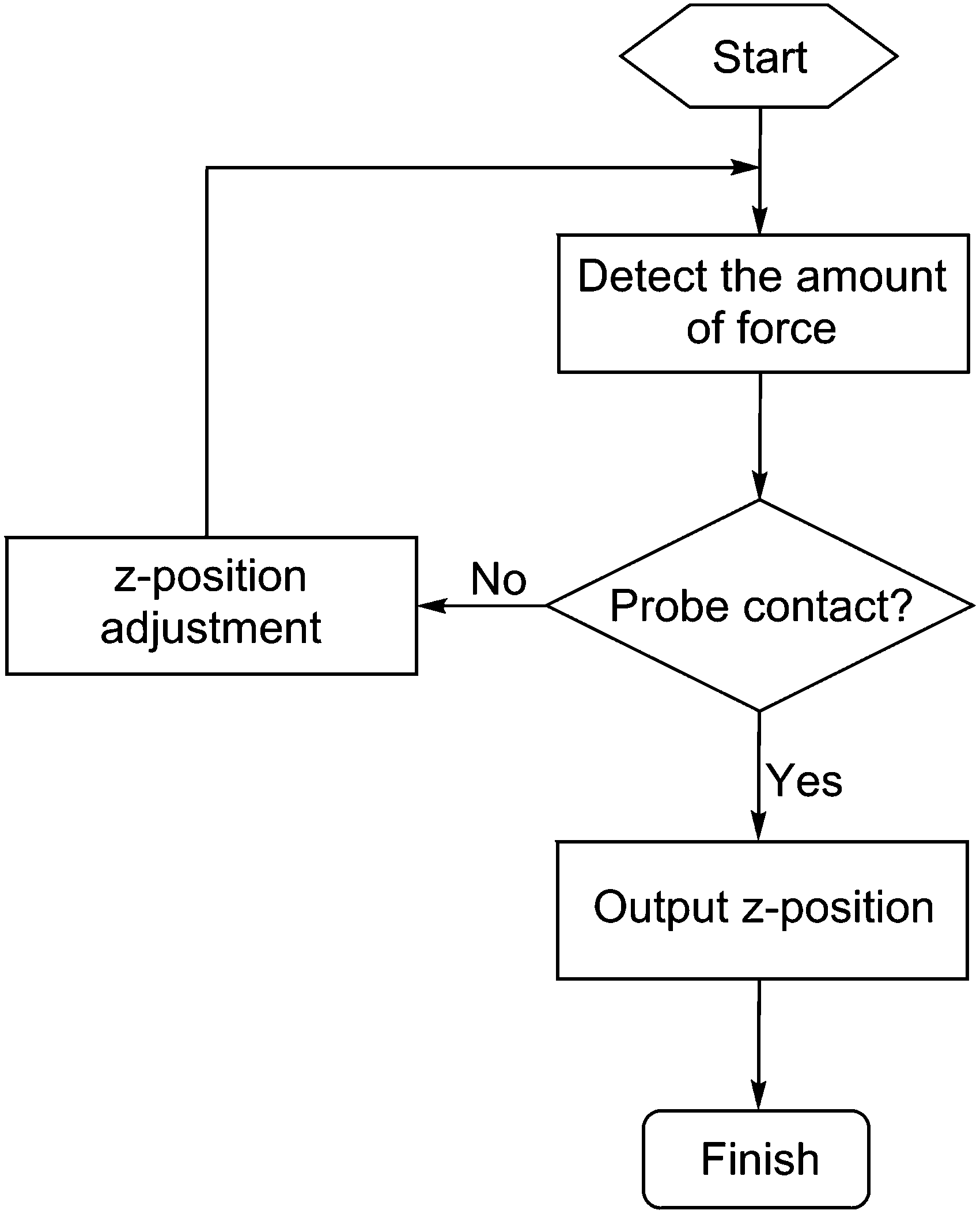 | ||
| Fig. 9 Flow chart to illustrate the z-position measurement procedure. | ||
 | ||
| Fig. 10 The flow chart of the procedure for obtaining the optimised stage tilt angle with respect to the maximum z-position. | ||
Fine optimisation is then performed using a series of z-position determinations with a ψ step size of 50 m° and N points of data (in this case N = 16) between ψ1 and ψ3 are recorded. The 150 m° “shifted” angles are then determined. Thus, starting with φ fixed to an arbitrary value in Step 1, the N points of data are acquired. The data fitted to two lines with the least-squares method,33 and their intersection calculated as (θoptimum1, φarbitrary). In Steps 2 to 4, the general process is repeated to determine the pairs of angles (θoptimum1 + 150, φoptimum1), (θoptimum2, φoptimum1 − 150) and (θoptimum2 − 150, φoptimum2), respectively. The final overall optimised angles are then calculated as the intersection of two lines drawn diagonally between the four points mentioned above.
Alignment was performed using the described algorithm followed by patterning with a predefined template to produce the desired pattern using the standard lithography software provided with the AFM. Patterning was undertaken at 40% relative humidity at 20 °C with a dwell time of 0.25 s per dot feature. The gold substrate was then imaged in lateral force mode. Where required, the substrate was subsequently etched for 4 min with a freshly made solution of equal parts 40 mM thiourea, 27 mM iron(III) nitrate nonahydrate and 100 mM hydrochloric acid. The substrate was then imaged under an optical microscope.
Acknowledgements
The authors acknowledge financial support from the UK Engineering and Physical Sciences Research Council (grants EP/K011685/1, EP/K024485/1) and a graduate studentship for JH. We also thank Andreas Lieb and Christian Bippes (Nanosurf) for technical advice.References
- L. Nicu and T. Leïchlé, J. Appl. Phys., 2008, 104, 111101 CrossRef PubMed.
- J. A. Liddle and G. M. Gallatin, Nanoscale, 2011, 3, 2679–2688 RSC.
- B. C. Janegitz, J. Cancino and V. Zucolotto, J. Nanosci. Nanotechnol., 2014, 14, 378–389 CrossRef CAS PubMed.
- B. D. Gates, Q. Xu, M. Stewart, D. Ryan, C. G. Willson and G. M. Whitesides, Chem. Rev., 2005, 105, 1171–1196 CrossRef CAS PubMed.
- R. Garcia, R. V. Martinez and J. Martinez, Chem. Soc. Rev., 2006, 35, 29–38 RSC.
- X. N. Xie, H. J. Chung, C. H. Sow and A. T. S. Wee, Mater. Sci. Eng., R, 2006, 54, 1–48 CrossRef PubMed.
- X. Zhou, F. Boey, F. Huo, L. Huang and H. Zhang, Small, 2011, 7, 2273–2289 CrossRef CAS PubMed.
- M. Tello, F. García and R. García, in Applied Scanning Probe Methods, ed. B. Bhushan and H. Fuchs, Springer, Berlin, 2006, pp. 137–158 Search PubMed.
- Z. Wei, D. Wang, S. Kim, S.-Y. Kim, Y. Hu, M. K. Yakes, A. R. Laracuente, Z. Dai, S. R. Marder, C. Berger, W. P. King, W. A. de Heer, P. E. Sheehan and E. Riedo, Science, 2010, 328, 1373–1376 CrossRef CAS PubMed.
- G. J. Leggett, Chem. Soc. Rev., 2006, 35, 1150–1161 RSC.
- D. S. Ginger, H. Zhang and C. A. Mirkin, Angew. Chem., Int. Ed., 2004, 43, 30–45 CrossRef PubMed.
- A. Lewis, Y. Kheifetz, E. Shambrodt, A. Radko, E. Khatchatryan and C. Sukenik, Appl. Phys. Lett., 1999, 75, 2689–2691 CrossRef CAS PubMed.
- K.-H. Kim, N. Moldovan and H. D. Espinosa, Small, 2005, 1, 632–635 CrossRef CAS PubMed.
- R. R. Gruter, J. Voros and T. Zambelli, Nanoscale, 2013, 5, 1097–1104 RSC.
- J. Haaheim and O. A. Nafday, Scanning, 2008, 30, 137–150 CrossRef CAS PubMed.
- M. Zhang, D. Bullen, S.-W. Chung, S. Hong, K. S. Ryu, Z. Fan, C. A. Mirkin and C. Liu, Nanotechnology, 2002, 13, 212–217 CrossRef CAS.
- D. Wouters and U. S. Schubert, Nanotechnology, 2007, 18, 485306 CrossRef.
- E. ul-Haq, Z. Liu, Y. Zhang, S. A. Alang Ahmad, L. S. Wong, J. K. Hobbs, G. J. Leggett, J. Micklefield, C. J. Roberts and J. M. R. Weaver, J. Mater. Res., 2011, 26, 2997–3008 CrossRef CAS.
- A. Safi, W. Kang, D. Czapleski, R. Divan, N. Moldovan and H. D. Espinosa, J. Micromech. Microeng., 2013, 23, 125014 CrossRef.
- W. P. King, T. W. Kenny, K. E. Goodson, G. L. W. Cross, M. Despont, U. T. Durig, H. Rothuizen, G. Binnig and P. Vettiger, J. Microelectromech. Syst., 2002, 11, 765–774 CrossRef CAS.
- K. Salaita, Y. Wang, J. Fragala, R. A. Vega, C. Liu and C. A. Mirkin, Angew. Chem., Int. Ed., 2006, 45, 7220–7223 CrossRef CAS PubMed.
- F. Huo, Z. Zheng, G. Zheng, L. R. Giam, H. Zhang and C. A. Mirkin, Science, 2008, 321, 1658–1660 CrossRef CAS PubMed.
- W. Shim, A. B. Braunschweig, X. Liao, J. Chai, J. K. Lim, G. Zheng and C. A. Mirkin, Nature, 2011, 469, 516–520 CrossRef CAS PubMed.
- F. Huo, G. Zheng, X. Liao, L. R. Giam, J. Chai, X. Chen, W. Shim and C. A. Mirkin, Nat. Nanotechnol., 2010, 5, 637–640 CrossRef CAS PubMed.
- Z. Xie, Y. Shen, X. Zhou, Y. Yang, Q. Tang, Q. Miao, J. Su, H. Wu and Z. Zheng, Small, 2012, 8, 2664–2669 CrossRef CAS PubMed.
- X. Liao, A. B. Braunschweig and C. A. Mirkin, Nano Lett., 2010, 10, 1335–1340 CrossRef CAS PubMed.
- J. Haaheim, V. Val, J. Bussan, S. Rozhok, J.-W. Jang, J. Fragala and M. Nelson, Scanning, 2010, 32, 49–59 Search PubMed.
- A. J. Senesi, D. I. Rozkiewicz, D. N. Reinhoudt and C. A. Mirkin, ACS Nano, 2009, 3, 2394–2402 CrossRef CAS PubMed.
- F. Brinkmann, M. Hirtz, A. M. Greiner, M. Weschenfelder, B. Waterkotte, M. Bastmeyer and H. Fuchs, Small, 2013, 9, 3266–3275 CAS.
- S. A. M. Carnally and L. S. Wong, Nanoscale, 2014, 6, 4998–5007 RSC.
- L. R. Giam, A. J. Senesi, X. Liao, L. S. Wong, J. Chai, D. J. Eichelsdoerfer, W. Shim, B. Rasin, S. He and C. A. Mirkin, Proc. SPIE, 2011, 8031, 803103 CrossRef PubMed.
- A. A. Tseng, Nano Today, 2011, 6, 493–509 CrossRef CAS PubMed.
- S. M. Stigler, Ann. Statist., 1981, 9, 465–474 CrossRef.
Footnote |
| † These authors contributed equally to this work. |
| This journal is © The Royal Society of Chemistry 2015 |