
 Open Access Article
 This Open Access Article is licensed under a
 Creative Commons Attribution 3.0 Unported Licence
Formation mechanism and optical characterization of polymorphic silicon nanostructures by DC arc-discharge†
Jieyi
Yu
a,
Jian
Gao
a,
Fanghong
Xue
a,
Xiuhong
Yu
 a,
Hongtao
Yu
b,
Xinglong
Dong
*a,
Hao
Huang
a,
Ang
Ding
ad,
Xie
Quan
b and
Guozhong
Cao
c
a,
Hongtao
Yu
b,
Xinglong
Dong
*a,
Hao
Huang
a,
Ang
Ding
ad,
Xie
Quan
b and
Guozhong
Cao
c
aKey Laboratory of Materials Modification by Laser, Ion and Electron Beams (Ministry of Education), School of Materials Science and Engineering, Dalian University of Technology, Dalian 116023, China. E-mail: dongxl@dlut.edu.cn
bKey Laboratory of Industrial Ecology and Environmental Engineering (Ministry of Education), School of Environmental Science and Technology, Dalian University of Technology, Dalian, 116024, China
cDepartment of Materials Science and Engineering, University of Washington, Seattle, WA 98195, USA
dNingbo Branch of China Academy Ordnance Science, 199 Lingyun Road, Ningbo, 315103, China
First published on 12th August 2015
Abstract
Silicon nanoparticles (Si NPs), silicon nanosheets (Si NSs), and silicon nanoribbons (Si NRs) were fabricated by means of DC arc-discharge under diverse atmospheres (hydrogen, mixtures of hydrogen and inert gas). It is shown that these as-prepared Si NPs are approximately 5–50 nm in diameter, Si NSs are about 10–30 nm in width and about 2.8 nm in thickness, and Si NRs consist of fine sheets with a length as long as 200 nm, width of 13 nm, and thickness of 3.1 nm. BET measurements reveal that the specific surfaces are 110.9, 108.8, and 164.2 m2 g−1 for Si NPs, Si NSs, Si NRs, respectively. Formation mechanisms for polymorphic Si nanostructures are elucidated, revealing that the anisotropic or isotropic growth of Si nanostructures is greatly induced by high energetic inert gas and hydrogen atoms, and finally results in the formation of polymorphic Si nanostructures. A visible down-shift of Raman frequency for these Si nanostructures is mainly attributed to the size effect. The band gaps are experimentally measured as 2.89 eV (Si NPs), 2.92 eV (Si NSs), and 3.02 eV (Si NRs) for direct transition, and 1.99 eV (Si NPs), 1.26 eV (Si NSs), and 1.36 eV (Si NRs) for indirect transition. These are noticeably enlarged with respect to bulk Si (1.1 eV).
Introduction
Silicon is one of the most abundant elements on Earth, with an extremely important role in nature and modern society. It has been studied intensively in the fields of condense matter physics, material science and engineering, and industrial semiconductors.1,2 In recent decades, silicon nanomaterials (like silicon nanoparticles and nanosheets) have attracted interest because of their quantum confinement effects, non-toxicity, high surface activity, biocompatibility, photostability, etc. They can be used, for example, in biosensors, cell imaging, lasers, or optical mixers.3–6 Silicon atoms form a face-centered cubic structure by sp3 hybridization, like diamond, with the result that synthesis of two-dimensional (2D) silicon nanosheets is difficult. A variety of approaches have been reported for preparing silicon nanoparticles, such as solution-based precursor reduction, precursor thermolysis and pyrolysis, and physical methods.1,7–11 Although synthesized silicon nanoparticles display high quantum yield, the synthesis methods rely on specialist reagents/reactors as well as the need for hazardous HF or HF–HNO3 to afford efficient control over particle size.7Two-dimensional silicon has attracted a lot of interest. It was expected to eliminate the difference between quantum theory in 0D or 1D nanomaterial and 3D macro block material. Lu et al. reported controlled synthesis of ultrathin Si nanosheets with a thickness of about 3.5 nm using graphene oxide nanosheets (GOs) as sacrificial templates.12 The size of the Si nanosheets could be controlled by use of GO sheets with different sizes. Free-standing and single-crystalline Si nanosheets, with a thickness of about 3 nm, can be synthesized by a chemical vapor deposition (CVD) process.13 The direct band gap of these Si nanosheets was 2.8 eV and the indirect band gap was 1.73 eV. Enhanced direct band gap transition was confirmed. Oxygen-free Si NSs, covered with organic groups and of 7.5 nm thickness, can be obtained by exfoliation of layered polysilane as a result of the reaction with n-decylamine and dissolution in chloroform.14 Its band gap was measured at 2.3 eV. Some fundamental properties of Si nanomaterials were also determined by Ikuno et al.15 Mg-doped silicon sheets capped with oxygen had been synthesized by Nakano et al. using a chemical exfoliation method.16 All of the investigations showed their features in fabrication of Si nanostructures. Synthesis of pure silicon sheets, especially silicene, is an attractive direction for current research,12–14,16 as efficient and simple synthesis methods are required.
Herein, physical vapor condensation, that is a DC arc-discharge method, is applied to fabricate diversified nanostructures of silicon, for example silicon nanoparticles (Si NPs), silicon nanosheets (Si NSs), and silicon nanoribbons (Si NRs). In our experiments, bulk silicon was used as the target to be evaporated and the atmosphere was pure hydrogen or a mixture of inert gas (argon or helium) and hydrogen. Arc-discharge plasma can be used to dominate the formation of Si nanostructures by adjusting the experimental conditions. The growth mechanisms and basic properties of these Si nanostructures are discussed in detail.
Results and discussion
A series of TEM images of the Si nanopowders are shown in Fig. 1a–f. Diverse morphologies of the Si nanostructures, that is particles, sheets, and ribbons, can be distinctly observed. Si NPs (Fig. 1a and b) consist of single-crystal particles of spherical shape with sizes ranging from 5 to 50 nm. The interplanar spacing of Si NPs is 3.1 Å, which represents the (111) lattice plane of bulk Si (Fig. 1b). Nitrogen adsorption results (Fig. S1a†) show that the specific surface area of Si NPs is about 110.9 m2 g−1. Si NSs (Fig. 1c and d) show a flaky shape with irregular edges, and a specific surface area of about 108.8 m2 g−1 (Fig. S1b†). The widths of Si NSs are in the range 10–30 nm, and its thickness is 2.8 nm as detected by AFM testing. As indicated in Fig. 1d, the interplanar spacing of Si NSs is about 3.1 Å, which is identical to that of (111) facets in Si NSs. Si NRs (Fig. 1e and f) are fiber-like shapes of about 13 nm width, more than 200 nm full length, and about 3.1 nm thickness (results from AFM testing). This is actually a kind of ribbon with thickness less than its diameter (the ratio of width over thickness is 4.2).17 The specific surface area of the Si NRs is 164.2 m2 g−1 (Fig. S1c†). From the detailed microstructures shown in Fig. 1f, Si NRs are multi-crystal (sheets) stacked ribbons resulting from anisotropic growth of Si. The interplanar spacing of Si NRs is also about 3.1 Å, which is in a good agreement with the distance between adjacent (111) lattice planes in Si NSs (Fig. 1f), suggesting that the NRs consist of smaller NSs through discernable interfaces. Furthermore, the growth direction of Si NRs has an angle (θ, as labeled in Fig. 1f) of about 20° to 〈111〉 crystal orientation of NSs and can be preliminarily determined as 〈112〉 direction,18 because the calculated angle between 〈111〉 and 〈112〉 direction is about 18°. Thin amorphous silicon oxide layers coated on all of the Si nanostructures are altered in thickness depending on the surface activity of fresh nanostructures formed in the passivation process, and this has influence on some basic properties of Si nanopowder products.19 It is interesting that these polymorphic nanostructures of silicon were controlled and induced by the preparation atmosphere, that is hydrogen and inert gases (Ar or He). The formation mechanism will be discussed in the following section. | ||
| Fig. 1 TEM and HRTEM images of (a and b) Si NPs, (c and d) Si NSs, and (e and f) Si NRs. | ||
AFM images of Si NSs and Si NRs are shown in Fig. 2a and c, respectively. The thickness of Si NSs was measured with a contact mode at intervals between the nanosheet and the substrate surface as shown in Fig. 2b, yielding an average value of 2.8 nm. The thickness of Si NRs was measured with a tapping mode from the distance between two red line segments (Fig. 2d), which is about 3.1 nm, less than its width of 13 nm as detected by HRTEM. Si NSs and Si NRs in this work are basically similar to the silicon nanosheets synthesized using graphene oxide as template.12 Nevertheless, the Si NRs actually consist of laterally assembled NSs along 〈112〉 crystal crystal orientation with an angle of about 20° to 〈111〉 direction of NSs.
 | ||
| Fig. 2 AFM images of (a) Si NSs, absorb onto a monocrystalline silicon wafer substrate, (c) Si NRs, absorb onto a crystal mica substrate, and (b), (d) are line profiles taken along the line in (a) and (c). | ||
XRD patterns of Si NPs, NSs, and NRs, as well as bulk silicon, are presented in Fig. 3. The characteristic diffraction peaks are confirmed as the silicon in cubic system (JCPDS 05-0565). Two features are found in the XRD peaks: first, all peaks of Si nanostructures are broader in comparison with those of bulk silicon, indicating that fine grains exist in the Si nanostructures; second, the strongest diffraction peak of (220) crystal face for bulk Si is changed to (111) in all Si nanostructures, representing anisotropic growth of grains in the Si nanostructures, particularly in the Si NRs sample as shown in the diffraction intensity ratios of (111) to (220) crystal faces. These ratios of I(111)/I(220) are 0.83, 1.56, 1.71, and 2.08 for bulk Si, Si NPs, Si NSs, and Si NRs, respectively. The formation of Si nanostructures is essentially a re-assembly of Si atoms under an atmosphere of hydrogen and inert gas. It is found that the nucleation and anisotropic growth of Si nanostructures are greatly influenced by such active and inert atoms.
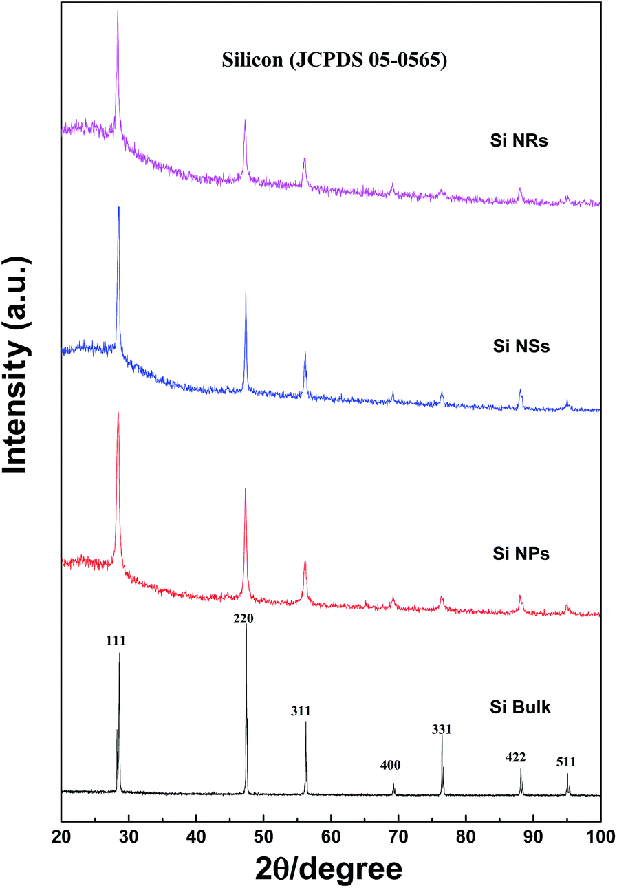 | ||
| Fig. 3 XRD patterns of Si bulk, Si nanostructures of NPs, NSs, and NRs. | ||
The schematic formation mechanisms for Si NPs, NSs, and NRs are presented in Fig. 4. The nucleation and growth of Si nanostructures have been influenced greatly by the presence of hydrogen and inert ions. Si has a face-centered cubic structure with the surface atomic density varying at different facets:
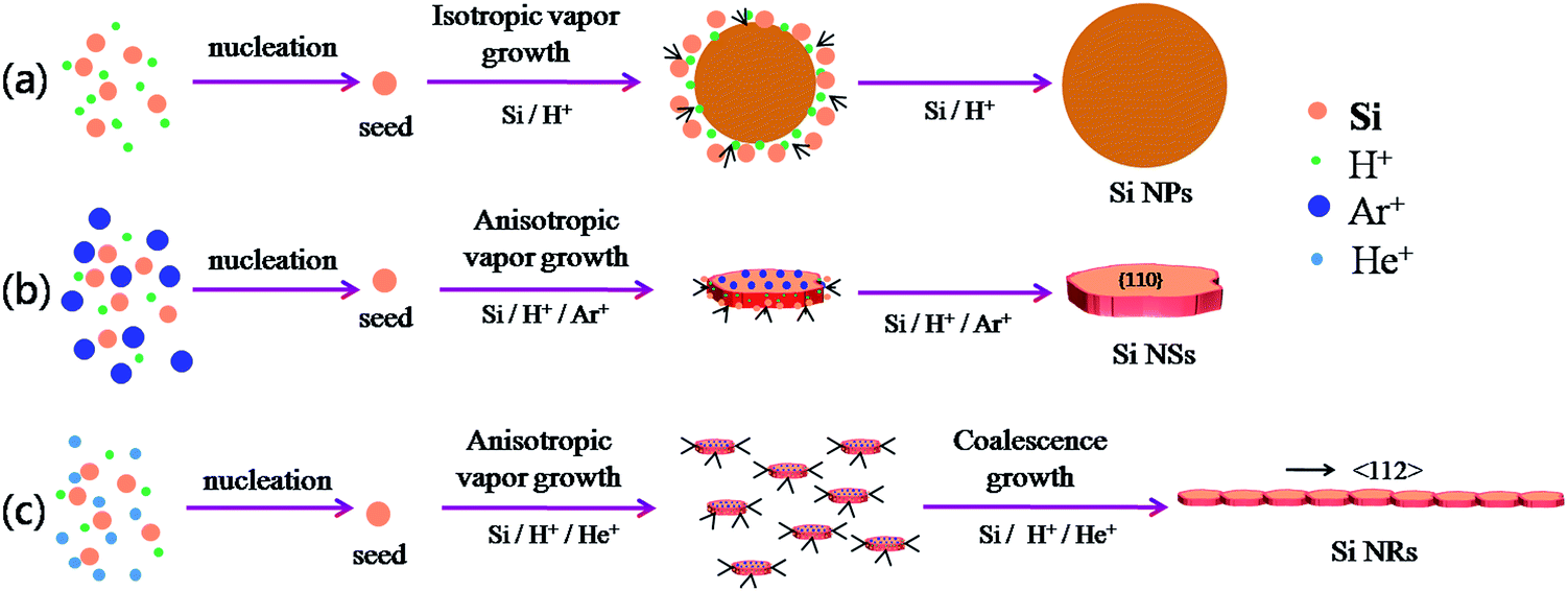 | ||
| Fig. 4 Schematic formation mechanism for Si nanostructures, (a) Si NPs; (b) Si NSs; (c) Si NRs. | ||
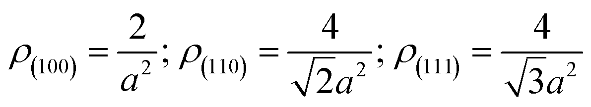
Without restructuring, relaxation, nor chemical or physical adsorption of heteroatoms or molecules, the surface energy of various facets can be calculated using the following formula:20a
 | (1) |
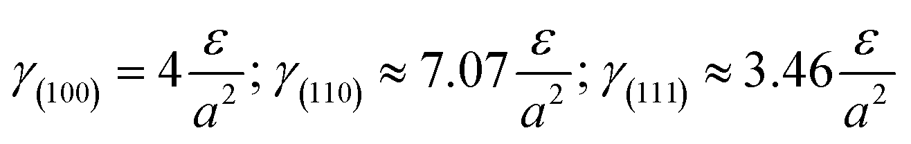
This means that if the outside faces of a Si single crystal consist of (111) crystal faces, the energy of such a monocrystalline will be the lowest and most stable, in other words, the crystallographic direction of 〈111〉 is the direction of Si single crystal with the slowest growth rate. Such a case is absolutely converted by the effects of H+, Ar+ or He+ ions in this work. Herein, the 〈111〉 becomes a favorable growth direction for Si NSs, the 〈112〉 direction favors growth of Si NRs, and the (110) facet is the outside surface of Si NSs. It is implied that the growth mechanisms for Si nanostructures would be greatly affected by the existence of H+, Ar+, or He+ ions and can induce isotropic growth of Si NPs and anisotropic growth of Si NSs and NRs.
In a process of arc-discharge, the arc flame is made up of inner, intermediate, and outer zones.21,22 Nucleation of a Si cluster is completed in the inner zone under a high concentration of Si atoms, and then grows further within the intermediate and outer zones.21–23 In a pure hydrogen atmosphere, H+ ions can promote evaporation of Si atoms by the high energy hydrogen plasma and quick transfer from molten silicon to outside space, and they can also equally affect growth of Si seeds in all directions by a weak bond between Si and H, which results in isotropic growth of Si nanoparticles (NPs) as illustrated in Fig. 4a.24,25 Here, H+ ions favor interaction with the high-energy faces of Si seed and slow the growth rate down, resulting in all growth rates of {111}, {100}, and {110} facets being nearly the same. For the atmosphere of mixed Ar and H2 with total gas pressure of 0.03 MPa, the content of H2 was reduced to 33%, resulting in reduction of its effect for isotropic growth. The anisotropic growth of Si crystallites had been forecast by the Periodic Bond Chain (PBC) theory,20b,26 in which {100} faces (flat surfaces, denoted as F-face) have one PBC running through, {110} stepped surfaces (S-faces) have two PBCs, and {111} kinked surfaces (K-face) have three PBCs. Both {110} and {111} faces have faster growth rate than {100} surface in a simple cubic crystal;20 however, the higher surface energy of (110) face than that of (111) induces preferential growth of (111) face (anisotropic growth) to be nanosheets as illustrated in Fig. 4b. Moreover, Ar+ ions can act as a condensed gas to collide and exchange energy with Si atoms, and initiate Si atoms for vapor growth on each face.27–29 For the mixed atmosphere of He and H2, the most different behavior between He+ and Ar+ ions is that He+ has greater efficiency on condensation and energy exchange because it has lighter atomic weight (4 mol g−1) than Ar+ (40 mol g−1), consequently smaller seeds (or sheets) of Si can be produced by He gas. Moreover, the lower diffusion coefficient of He than that of Ar30,31 can persevere with condensation on small-sized sheets and facilitate a secondary nucleation (coalescence growth), accordingly the stacked fine sheets are regularly formed into a ribbon-shape as illustrated in Fig. 1f and 4c. Such a coalescence growth develops (stacks) the small sheets along 〈112〉 direction with an angle (θ) of about 20° to 〈111〉 direction as shown in Fig. 1f.
Si NPs are a result of isotropic growth under the equivalent effect of H+ ions in all directions (vapor growth mechanism); Si NSs undergo anisotropic growth along 〈111〉 direction under the selective influence of Ar+ ions (vapor growth mechanism) with the top surface terminated on the (110) facet; Si NRs undergo anisotropic growth, with the influence of He+ ions resulting in fine sheets that stack up into ribbon shapes along 〈112〉 direction (the coalescence growth mechanism) with the top surface of (110) facet. It is significant that the preparation atmosphere (hydrogen, inert gases) has a great influence on the ultimate morphologies of Si nanostructures. These interpretations are consistent with the results of XRD and HRTEM measurements. Moreover, it is found that the existence of inert gas in the atmosphere can improve the product yield of Si nanopowders as shown in Table 1. In this work, the total gas pressures were the same (0.03 MPa) for production of the three kinds of Si nanostructures, so the vapor pressure of Si atoms created can be considered the same and any influence on production yield can be ignored. A noticeable effect comes from He gas. As mentioned above, He atoms have greater efficiency on condensation of nanoribbons through a coalescence growth mechanism in which a great deal of fine sheets of Si are consumed. In comparison with solitary vapor growth, the coalescence growth can be considered to be the dominant factor on the product yield through rapid consumption of Si atoms and fine sheets, with simultaneous acceleration of evaporation of bulk Si.
| Samples | Gas pressure [MPa] | Arc voltage [V] | Arc current [A] | Morphology | Yield [g h−1] | ||
|---|---|---|---|---|---|---|---|
| H2 | Ar | He | |||||
| 1 | 0.03 | 0 | 0 | 20 | 90 | Nanoparticles | 3.1 |
| 2 | 0.01 | 0.02 | 0 | 20 | 90 | Nanosheets | 8.4 |
| 3 | 0.01 | 0 | 0.02 | 20 | 90 | Nanoribbons | 18.6 |
As shown in Fig. 5, Raman spectra in the range of 100–1200 cm−1 wave numbers were measured for the Si nanostructures of NPs, NSs, NRs, and bulk Si. The features of vibrating modes, for example first order optical phonon (TO, zone center transverse optical phonon), two transverse acoustic phonons (2TA) and two transverse optical phonons (2TO), are labeled in the figure. As a counterpart for comparison, bulk Si exhibits a strong Raman peak at 520 cm−1 with FWHM (full width at half maximum) of 10 cm−1, which is ascribed to the scattering of first order optical phonon (TO) and a response of Si–Si stretching vibration. The TO peak of Si NPs is marginally down-shifted to 518 cm−1 with FWHM of 7.9 cm−1, but greatly shifted to 500 cm−1 (FWHM of 19 cm−1) for Si NSs and to 498 cm−1 (FWHM of 22 cm−1) for Si NRs, with a prominent diversity emerging in the Raman scattering of Si nanostructures consisting of fine sheets (NSs and NRs). Bulk Si is a crystal with a regular tetrahedron structure, each Si atom is surrounded by four Si atoms and its bonds form a covalent bond; the length and bond angle of bonds are long-range order.32 Si NPs are monocrystalline with size up to a maximum of 50 nm, a periodic boundary condition (translation symmetry) in such bigger nanoparticles can be recognized similar to that of bulk Si and a comparable TO peak of Raman scattering occurred between Si NPs and bulks.
 | ||
| Fig. 5 Raman spectra for bulk Si, Si NPs, Si NSs, and Si NRs. The inset figure is an enlargement of the peaks framed in dotted rectangle. | ||
The size effect on Raman frequency becomes pronounced in Si NSs and NRs, with down-shifts of 19 and 22 cm−1 wave numbers in comparison with bulk Si, respectively. As confirmed by AFM and HRTEM measurements, the limited size or thickness of Si NSs and NRs are 2.8 and 3.1 nm, with a breakdown of the periodic boundary condition occurring and influencing the behavior of first order optical phonon. It is thought that the length and angle of bonds in Si NSs and NRs vary with respect to bulk, an aberration of translational symmetry arises, and the correlation region becomes smaller as well as localization of the correlation function. For Raman scattering, when the correlation length is less than one-tenth of light wavelength, the vibration mode evolves into a localized mode.32 This is the main reason for the prominent down-shift of Raman frequency and broadening of FWHM (more than 20 cm−1), and was proved theoretically by Faraci et al.33 The down-shift of Raman wave numbers also can be considered to result from the phonon confinement effect in two-dimensional nanoscale Si crystals.12,34,35 The phonons in nanostructures are recognized to be localized in phonon potential wells. For a two-dimensional well, movement in the z direction of electrons with two-dimensional sub-band energy is frozen, meaning electron motion is in the plan.32 The phonon scattering will not be limited to the center of the Brillouin zone, and phonon dispersion near the zone center must also be considered. The expanded FWHM of the TO peak for the Si NSs and NRs is also considered to be caused by the phonon confinement effect. In Fig. 6, XPS spectra are used to detect the surface composition and chemical environment on the Si NPs, NSs, and NRs. The feature of O 1s electrons at binding energy of 532.6 eV (Fig. 6d) indicates that slight oxidation (as exposed to air in the passivation process) occurred on the surfaces of Si nanostructures,36 which is further confirmed by the binding energies of Si 2p electrons (as seen in Fig. 6a–c). All Si nanostructures show the same peak of elemental Si (Si0) (at 99.27, 99.37, and 99.6 eV), which is attributed to the Si cores of the NPs, NS,s and NRs. Nonetheless, the silicon oxides passivated on these samples are complex and quite different, that is 101.77 and 103.17 eV (for Si NPs); 103.0 and 103.48 eV (for Si NSs); and 102.9 and 103.4 eV (for Si NRs), implying that the three kinds of Si nanostructures had suffered from the different passivation because of their dissimilar surface activities. The complex silicon oxides are considered to be oxygen-doped oxides because their binding energies for O 1s electrons are lower than the 104 eV for pure SiO2.37 In Fig. 6a–c, the intensity (using area of peak) ratios of SiO/Si are 1.3 (for Si NPs), 4.3 (for Si NSs), and 6.2 (for Si NRs), respectively. If these ratio data are normalized with respective specific surface areas, they are 0.0117 for Si NPs, 0.0395 for Si NSs, and 0.0378 for Si NSs, suggesting that NSs and NRs have a similar thickness of oxide layer on them, and that this is three times that of NPs. Such estimation of the thickness of oxide layers can be connected to the surface activities of Si nanostructures, and agrees with the results of TEM and AFM measurements.
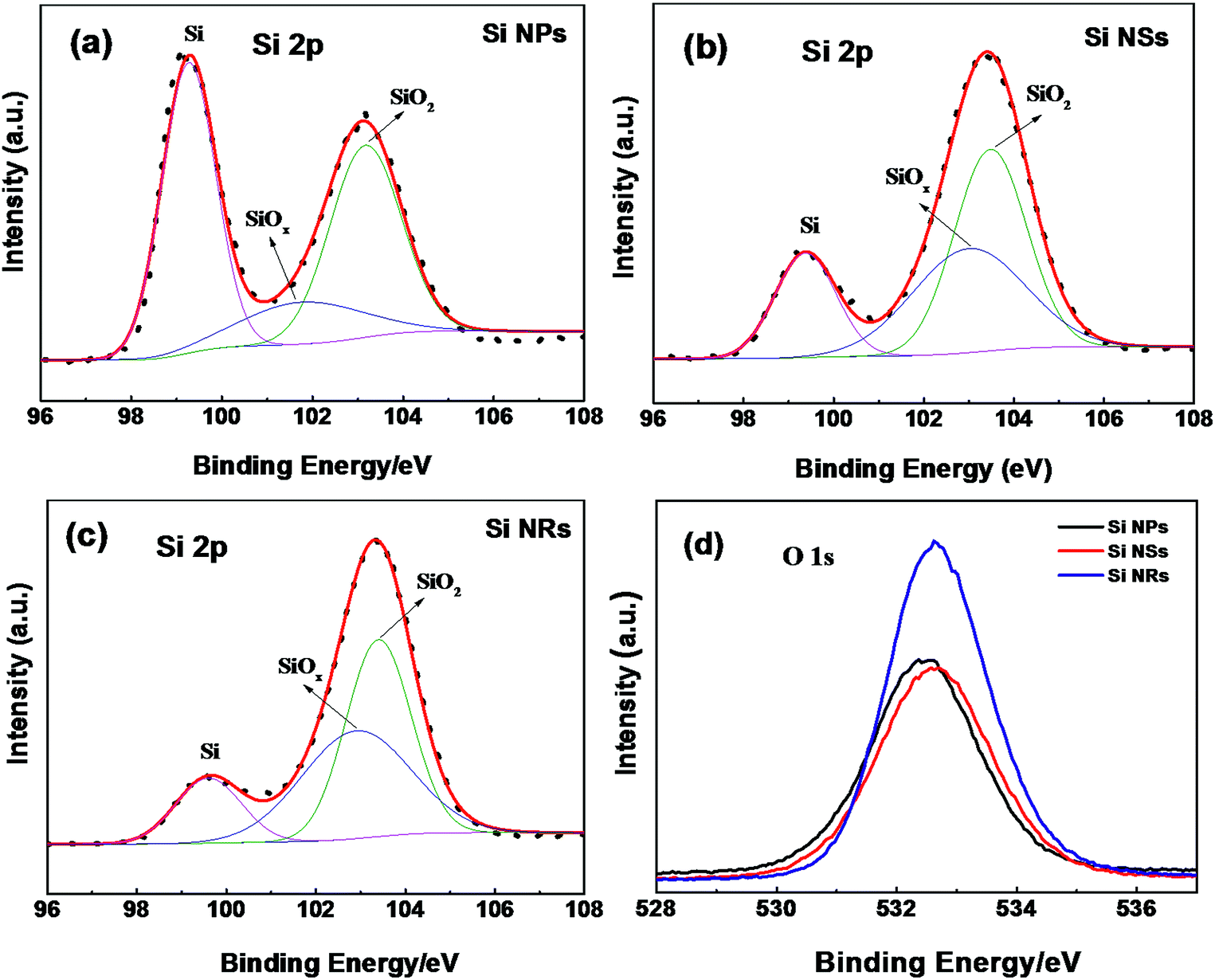 | ||
| Fig. 6 XPS spectra for Si 2p electrons of (a) Si NPs, (b) Si NSs, and (c) Si NRs, (d) O 1s electrons of the three samples. The experimental results are represented by dots, fitted to the solid lines. | ||
UV-visible (UV-vis) absorbance of Si NPs, NSs, and NRs were measured, as shown in Fig. 7a. The concentration of solution is quite low and only the Si nanostructures with smaller sizes could be suspended steadily in solution. It is anticipated that the UV-vis absorbance mainly originates from the Si cores and interfaces in nanostructures. As one may forecast, Si NPs display stronger absorption, particularly in the UV range, than Si NSs and NRs, because of its relatively larger size. Two peaks can be identified at about 380 and 300 nm for Si NPs, but both are faint (around 308 and 249 nm) for Si NSs and NRs. In the range of visible light, the absorptions for all Si samples become weak and comparable at the tails, implying inhomogeneous distribution of the sizes in all Si nanopowders.38 The direct band gaps (Ed) were obtained by linear extrapolation to zero in the plots of (αhν)2versus photon energy (Fig. 7b), these are 2.89, 2.92, and 3.02 eV for Si NPs, NSs, and NRs, respectively. This extrapolation method is controversial, but can be used to roughly appraise the band gap. These band gaps approximate to the free-standing Si NSs (2.8 eV, 3.0 nm in thickness),13 Mg-doped Si NSs (2.9 eV, 0.37 nm in thickness),16 and a little bigger than that covered with organic groups (2.3 eV, 7.5 nm in thickness).14 From results reported above as well on Si quantum dots, it can be concluded that the band gap will be bigger than 2.5 eV if the size is smaller than 5 nm. With respect to bulk Si (1.1 eV in Ei), noticeable blue-shifts of band gap are found for these Si nanostructures and have been reported in the literature, for example silicone nanowires39–41 and quantum dots.40–43 Such an enhancement in band gap is also considered from the quantum confinement effect,41–43 or a compressive strain determined by surface tension in Si nanosheets which can induce an indirect-direct band gap transition.13 The indirect band gaps (Ei) were obtained by linear extrapolation to zero in the plots of (αhν)1/2versus photon energy (Fig. 7c), these are 1.99, 1.26, and 1.36 eV for Si NPs, NSs, and NRs, respectively. The oxide layer on these Si nanostructures may have a negligible effect on these calculated band gaps. It was reported that the oxygen-terminated layers on Si quantum dots usually exhibit a band gap shifted to the red (about 1 eV) compared with those capped with hydrogen.44
 | ||
| Fig. 7 (a) UV-visible absorption spectra; the plots of (b) (αhν)2 (n = 1/2), and (c) (αhv)1/2 (n = 2) versus photon energy for Si NPs, NSs, and NRs at room-temperature, respectively. | ||
Experimental
Synthesis of Si nanomaterials
In our early research, the DC arc-discharge plasma method was adopted to fabricated metal-based nanoparticles (such as Fe, Ni, Co, Cu, Mg, etc.),45–47 carbon-coated nanocapsules,48,49 graphene,50 and silicon nanosheets.51 In this work, bulk silicon (raw material) served as an anode, while a tungsten rod was a cathode in the arc-discharge. Synthesis conditions for Si nanostructured samples are shown in Table 1. The arc current was set at 90 A and the voltage was maintained at about 20 V. The atmosphere was the key factor in control of the morphologies of Si nanomaterials. Pure hydrogen atmosphere favors formation of nanoparticles, whereas a mixture of H2 and inert gas (Ar or He) promotes anisotropic growth of Si (nanosheets or nanoribbons). After the working chamber was cooled to room-temperature, a trace of oxygen gas was deflated into the chamber to form a thin layer of Si oxides on the nanopowders, which can protect from further oxidization. All Si nanopowder products were collected from the roof of the evaporation chamber in an air environment.Characterization
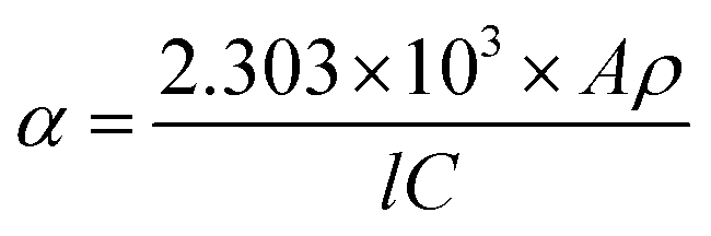
The morphologies and structures of Si nanostructured samples were characterized by Transmission Electron Microscopy (TEM, Tecnai2 20 S-TWIN, 200 keV). The testing samples were prepared by dropping a dilute solution of Si nanopowders in ethanol onto a Cu grid membrane. Atomic Force Microscopy (AFM) was recorded on DI-Multimode NS3A-02 using contact mode or Agilent PicoPlus II using tapping mode. The AFM testing samples were prepared by dropping a dilute solution of Si nanopowders in ethanol onto a crystal mica substrate. The phases of Si nanopowders were confirmed by X-ray diffraction (XRD, PANalytical Empyrean) using Cu Kα radiation (λ = 1.5416 Å). Specific surface area of Si nanopowders was tested by Brunauer Emmett Teller (BET) measurement on Quantachrome Autosorb-1 MP under a constant temperature of 77.3 K. Raman spectra were recorded with a laser excitation wavelength of 632.8 nm. X-ray Photoelectron Spectroscopy (XPS, Thermo Escalab 250Xi) utilizing monochromatic Al Kα (hν = 1486.6 eV) radiation as theta probe was adopted to analyze the surface species on Si nanopowders, and the spectra were calibrated to the C 1s emission arising from adventitious hydrocarbons (284.8 eV).UV-Visible (UV-vis) absorption spectra of the Si nanostructures were measured on a Lamda 950. For measurements, Si nanopowders were ultrasound-dispersed in deionized water to a concentration of 0.1 mg mL−1. The absorption coefficient α and the optical band gap Eg were determined by measured absorbance using the following equation:13,52,53
 | (2) |
| αhν ∝ (hν − Eg)n | (3) |
Conclusions
In conclusion, a simple strategy has been developed to synthesize Si nanomaterials in morphologies of particle, sheet, and ribbon, via a DC arc-discharge method by optimizing the evaporation conditions. Si NPs are synthesized in simplex H2 gas, Si NSs in a mixture of H2 and Ar, and Si NRs in the atmosphere by replacing Ar with He gas. Pure H2 favors isotropic growth of Si nanoparticles, whereas inert gases induce anisotropic growth of Si NSs and NRs. All Si nanostructures are core–shell type structures with Si core and SiOx-shell. The quantity of silicon oxide shells on Si cores is internally identical to the specific surfaces of Si nanostructures, these are 110.9 m2 g−1 (for Si NPs), 108.8 m2 g−1 (for Si NSs), and 164.2 m2 g−1 (for Si NRs). A phonon confinement effect is found and gives rise to a down-shift of Raman frequencies for Si nanostructures. Direct band gaps are calculated as 2.89 eV (Si NPs), 2.92 eV (Si NSs), and 3.02 eV (Si NRs), and indirect band gaps are 1.99 eV (Si NPs), 1.26 eV (Si NSs), and 1.36 eV (Si NRs).Acknowledgements
Financial support from National Basic Research Program of China (Grant No. 2011 CB936002); the Fundamental Research Funds for the Central Universities (2012DUT12RC (3) 101); and National Natural Science Foundation of China (No. 51271044, 51331006). We are very grateful for the help of Professor Yinong Wang in the analysis of crystal structure.References
- B. K. Teo and X. H. Sun, Chem. Rev., 2007, 107, 1454 CrossRef CAS PubMed.
- W. Luo, X. F. Wang, C. Meyers, N. Wannenmacher, W. Sirisaksoontorn, M. M. Lerner and X. L. Ji, Sci. Rep., 2013, 3(2222), 1 Search PubMed.
- S. Dhanekar and S. Jain, Biosens. Bioelectron., 2013, 41, 54 CrossRef CAS PubMed.
- J. Ge, P. Chen, Q. Jia, W. Liu, H. Zhou, B. Zhou, Q. Liu and P. Wang, RSC Adv., 2015, 5, 35291 RSC.
- G. de Valicourt, A. L. Liepvre, F. Vacondio, C. Simonneau, M. Lamponi, C. Jany, A. Accard, F. L. Elarge, D. Make, F. Poingt, G. H. Duan, J. M. Fedeli, S. Messaoudene, D. Bordel, L. Lorcy, J. C. Antona and S. Bigo, Opt. Express, 2012, 20, B552 CrossRef CAS PubMed.
- E. J. Henderson, A. J. Shuhendler, P. Prasad, V. Baumann, F. Maier-Flaig, D. O. Faulkner, U. Lemmer, X. Y. Wu and G. A. Ozin, Small, 2011, 7, 2507 CAS.
- J. G. C. Veinot, Chem. Commun., 2006, 4160 RSC.
- J. M. Buriak, Chem. Rev., 2002, 102, 1271 CrossRef CAS PubMed.
- B. D. Rowsell and J. G. C. Veinot, Nanotechnology, 2005, 16, 732 CrossRef CAS.
- J. D. Holmes, K. J. Ziegler, R. C. Doty, L. E. Pell, K. P. Johnston and B. A. Korgel, J. Am. Chem. Soc., 2001, 123, 3743 CrossRef CAS PubMed.
- G. Belomoin, J. Therrien, A. Smith, S. Rao and R. Twesten, Appl. Phys. Lett., 2002, 80, 841 CrossRef CAS.
- Z. Y. Lu, J. X. Zhu, D. H. Sim, W. W. Zhou, W. H. Shi, H. H. Hng and Q. Y. Yan, Chem. Mater., 2011, 23, 5293 CrossRef CAS.
- U. Kim, I. Kim, Y. H. Park, K. Y. Lee, S. Y. Yim, J. G. Park, H. G. Ahn, S. H. Park and H. J. Choi, ACS Nano, 2011, 5, 2176 CrossRef CAS PubMed.
- H. Okamoto, Y. Kumai, Y. Sugiyama, T. Mitsuoka, K. Nakanishi, T. Ohta, H. Nozaki, S. Yamaguchi, S. Shirai and H. Nakano, J. Am. Chem. Soc., 2010, 132, 2710 CrossRef CAS PubMed.
- T. Ikuno, H. Okamoto, Y. Sugiyama, H. Nakano, F. Yamada and I. Kamiya, Appl. Phys. Lett., 2011, 99, 1 CrossRef.
- H. Nakano, T. Mitsuoka, M. Harada, K. Horibuchi, H. Nozaki, N. Takahashi, T. Nonaka, Y. Seno and H. Nakamura, Angew. Chem., 2006, 118, 6451 ( Angew. Chem., Int. Ed. , 2006 , 45 , 6303 ) CrossRef.
- W. Shi, H. Peng, N. Wang, C. P. Li, L. Xu, C. S. Lee, R. Kalish and S. T. Lee, J. Am. Chem. Soc., 2001, 123, 11095 CrossRef CAS PubMed.
- D. P. Wei and Q. Chen, J. Phys. Chem. C, 2008, 112, 15129 CAS.
- R. P. Wang, G. W. Zhou, Y. L. Liu, S. H. Pan, H. Z. Zhang, D. P. Yu and Z. Zhang, Phys. Rev. B: Condens. Matter Mater. Phys., 2000, 61, 16827 CrossRef CAS.
- (a) G. Z. Cao and Y. Wang, in Nanostructures and Nanomaterials: Synthesis, Properties, and Applications, World Scientific, Hackensack, 2nd edn, 2011, ch. 2, pp. 21–23 Search PubMed; (b) G. Z. Cao and Y. Wang, in Nanostructures and Nanomaterials: Synthesis, Properties, and Applications, World Scientific, Hackensack, 2nd edn, 2011, ch. 4, pp. 152–153 Search PubMed.
- S. Yatsuya, S. Kasukabe and R. Uyeda, Jpn. J. Appl. Phys., 1973, 12, 1675 CrossRef CAS.
- S. Kasukabe, S. Yatsuya and R. Uyeda, Jpn. J. Appl. Phys., 1974, 13, 1714 CrossRef CAS.
- Y. Saito, S. Yatsuya, K. Mihama and R. Uyeda, Jpn. J. Appl. Phys., 1978, 17, 291 CrossRef CAS.
- D. E. Grove, U. Gupta and A. W. Castleman Jr, ACS Nano, 2010, 4, 49 CrossRef CAS PubMed.
- N. Radenović, W. V. Enckevort and E. Vlieg, J. Cryst. Growth, 2004, 263, 544 CrossRef.
- P. Hartman and W. G. Perdok, Acta Crystallogr., 1955, 8, 49 CrossRef.
- A. M. Morales and C. M. Lieber, Science, 1998, 279, 208 CrossRef CAS PubMed.
- C. M. Lieber, Solid State Commun., 1998, 107, 607 CrossRef CAS.
- J. Hu, T. W. Odom and C. M. Lieber, Acc. Chem. Res., 1999, 32, 435 CrossRef CAS.
- T. Ohno, S. Yatsuya and R. Uyeda, Jpn. J. Appl. Phys., 1976, 15, 1213 CrossRef CAS.
- T. Hayashi, T. Ohno, S. Yatsuya and R. Uyeda, Jpn. J. Appl. Phys., 1977, 16, 705 CrossRef CAS.
- S. L. Zhang, in Raman spectroscopy and its application in nanostructures, Wiley, Hoboken, 1st edn, 2012, ch. 7, p. 241 Search PubMed.
- G. Faraci, S. Gibilisco, A. R. Pennisi and C. Faraci, J. Appl. Phys., 2011, 109, 074311 CrossRef.
- G. Faraci, S. Gibilisco, P. Russo and A. R. Pennisi, Phys. Rev. B: Condens. Matter Mater. Phys., 2006, 73, 0333071 CrossRef.
- C. Meier, S. Luttjohann, V. G. Kravets, H. Nienhaus, A. Lorke and H. Wiggers, Phys. E, 2006, 32, 155 CrossRef CAS.
- Y. X. Zhang, X. Han, R. H. Liu, Y. Liu, H. Huang, J. M. Zhang, H. Yu and Z. H. Kang, J. Phys. Chem. C, 2012, 116, 20363 CAS.
- H. Nakano, M. Nakano, K. Nakanishi, D. Tanaka, Y. Sugiyama, T. Ikuno, H. Okamoto and T. Ohta, J. Am. Chem. Soc., 2012, 134, 5452 CrossRef CAS PubMed.
- C. C. Huang, K. Y. Chuang, C. J. Huang, T. M. Liu and C. S. Yeh, J. Phys. Chem. C, 2011, 115, 9952 CAS.
- J. D. Holmes, K. P. Johnston, R. C. Doty and B. A. Korgel, Science, 2000, 287, 1471 CrossRef CAS PubMed.
- D. D. D. Ma, C. S. Lee, F. C. K. Au, S. Y. Tong and S. T. Lee, Science, 2003, 299, 1874 CrossRef CAS PubMed.
- T. Takagahara and K. Yakeda, Phys. Rev. B: Condens. Matter Mater. Phys., 1992, 46, 15578 CrossRef CAS.
- Z. Kang, C. H. A. Tsang, Z. Zhang, M. Zhang, N. Wong, J. A. Zapien, Y. Shan and S. T. Lee, J. Am. Chem. Soc., 2007, 129, 5326 CrossRef CAS PubMed.
- Z. Kang, Y. Liu, C. H. A. Tsang, D. D. D. Ma, X. Fan, N. Wong and S. T. Lee, Adv. Mater., 2009, 21, 661 CrossRef CAS.
- M. V. Wolkin, J. Jorne, P. M. Fauchet, G. Allan and C. Delerue, Phys. Rev. Lett., 1999, 82, 197 CrossRef CAS.
- X. L. Dong, Z. D. Zhang, X. G. Zhao and Y. C. Chuang, J. Mater. Res., 1999, 14, 398 CrossRef CAS.
- X. L. Dong, Z. D. Zhang, S. R. Jin and B. K. Kim, J. Magn. Magn. Mater., 2000, 210, 143 CrossRef CAS.
- J. P. Lei, H. Huang, X. L. Dong, X. G. Zhu, B. Lu and M. K. Lei, J. Nanosci. Nanotechnol., 2009, 9, 7503 CAS.
- B. Lu, H. Huang, X. L. Dong and J. P. Lei, J. Phys. D: Appl. Phys., 2010, 43, 105403 CrossRef.
- X. F. Zhang, X. L. Dong, H. Huang, D. K. Wang, B. Lv and J. P. Lei, Nanotechnology, 2007, 18, 275701 CrossRef.
- G. F. Guo, H. Huang, F. H. Xue, C. J. Liu, H. T. Yu, X. Quan and X. L. Dong, Surf. Coat. Technol., 2013, 228, S120 CrossRef CAS.
- X. H. Yu, F. H. Xue, H. Huang, C. J. Liu, J. Y. Yu, Y. J. Sun and X. L. Dong, Nanoscale, 2014, 6, 6860 RSC.
- Z. Wang, Z. Quan and J. Lin, Inorg. Chem., 2007, 45, 5237 CrossRef PubMed.
- L. Yin, Y. Wang, G. Pang, Y. Koltypin and A. Gedanken, J. Colloid Interface Sci., 2002, 246, 78 CrossRef CAS PubMed.
Footnote |
| † Electronic supplementary information (ESI) available. See DOI: 10.1039/c5ra11738k |
| This journal is © The Royal Society of Chemistry 2015 |