
Flexible quantum dot light emitting diodes based on ZnO nanoparticles†
Jiangyong
Pan
a,
Jing
Chen
*a,
Qianqian
Huang
a,
Qasim
Khan
a,
Xiang
Liu
a,
Zhi
Tao
a,
Wei
Lei
*a,
Feng
Xu
a and
Zichen
Zhang
*b
aSchool of Electronic Science and Engineering, Southeast University, Nanjing, China 210096. E-mail: chenjing@seu.edu.cn; lw@seu.edu.cn
bState Key Laboratory of Precision Measurement Technology and Instruments, Collaborative Innovation Center for Micro/Nano Fabrication, Device and System, Department of Precision Instrument, Tsinghua University, Beijing 100084, China. E-mail: zz241@tsinghua.edu.cn
First published on 16th September 2015
Abstract
Flexible quantum dot light emitting diodes (QLEDs) have attracted extensive attention owing to the advantages of foldability and their broad application in flexible display devices. In this work, we report high performance, mechanically flexible QLEDs based on ZnO nanoparticles used as an electron transfer layer (ETL). The QLEDs have been fabricated on poly(ethylene-terephthalate) (PET) substrates utilizing a unique structure consisting of bilayered hole transport films and ZnO nanoparticles acting as an ETL to improve the device performance owing to its appropriate energy band position and high charge mobility. The QLEDs exhibited high performance, such as a lowered turn on voltage of 1.6 V and improved current and power efficiencies of 5.20 cd A−1 and 1.80 lm W−1, respectively. They presented good flexibility with a critical bending radius of 4.5 mm, suggesting the broad application potential of flexible QLEDs.
1. Introduction
Colloidal quantum dots (QDs) are considered to be a rising candidate for new-generation light-emitting materials because they possess unique properties such as tunable emission wavelengths (because of the quantum confinement effect), highly saturated emission color, narrow emission with a small full width at half maxima (FWHM), solution processability, and compatibility with flexible substrates.1,2 Since the first report of electrically driven quantum dot LEDs (QLEDs) utilizing CdSe QDs in 1994,3 QLEDs have received considerable attention for academic research and potential commercialization. After about two decades of research and development, QLEDs are reaching the performance of organic LEDs (OLEDs) and emerging as a candidate for single-material, full-color light sources.4–7 It is noted that in the past few years, much effort has been made to improve the efficiency of QLEDs by optimization of the active materials and the employment of novel structures. For example, in a review report, Reineke has summarized the major structural improvements of QDs such as the adoption of a core–shell configuration, the passivation of surface trap states, and the engineering of the electronic and chemical properties of the organic ligands surrounding the QDs, and has mentioned the major superiority of QLEDs over OLEDs in spectral purity.8 Yang et al. have demonstrated a full series of blue, green and red QLEDs with high efficiencies, which can be achieved by optimizing the nanostructure of the quantum dots, especially the composition of the graded intermediate shell and the thickness of the outer shell.9 As for the employment of novel structures, Dai et al. have reported a highly efficient QLED by inserting an insulating layer between the quantum dot layer and the oxide electron-transport layer to optimize the charge balance in the device.6 In addition, Tu et al. demonstrated surface plasmon-enhanced electroluminescence (EL) in QLEDs by incorporating Au NPs into the ZnO electron transport layer, which provided strong coupling between localized surface plasmons (LSPs) in the Au NPs and excitons in the QDs.10Despite much progress in the improvement of device performance, QLEDs still face many problems, especially low stability, including drastic efficiency roll-off at high current densities and low operational lifetime,6 lower EL efficiencies compared with those of OLEDs due to the limitations in electrical properties and the device structure11 and high production cost due to the use of vacuum-requiring thermal evaporation.8
Up to now, most of the investigated devices have been fabricated on rigid substrates, such as glasses.11,12 Flexibility is one of the key elements for future information displays,13,14 especially in intelligent household electrical appliances. The key advantages of flexible electronics, compared with current silicon technologies, are low-cost manufacturing and inexpensive flexible substrates through the use of roll-to-roll (or sheet-to-sheet) fabrication methods with high yield and high throughput. Recently, Yang et al. have reported highly efficient, large-area QLED tapes emitting in full color with top-emitting design and polyimide tapes as flexible substrates.7 Panzer et al. have demonstrated tunable infrared emission from printed colloidal quantum dot/polymer composite films on flexible substrates. The display operates by optical down conversion of AC-driven blue phosphor electroluminescence using different-sized, IR-emitting colloidal quantum dots.15 In addition, Kim et al. demonstrated QLEDs which use InP/ZnSe/ZnS multi shell colloidal QDs prepared by a simple heating-up synthesis, which were fabricated on a polyethylene naphthalate (PEN) substrate for flexible optoelectronic devices.16 However, the optoelectronic properties of QLEDs on flexible substrates have not been fully investigated yet and they also face many problems such as high turn on voltage, low device efficiency and instability.
In this work, we report flexible QLEDs which have been designed and fabricated over indium tin oxide (ITO)-coated polyethylene terephthalate (PET) substrates. The adoption of 2.9 nm-sized ZnO NPs as an ETL and a dual HTL in the structure is to balance the charge transfer rate. A lowered turn on voltage of 1.6 eV, improved efficiency of 5.20 cd A−1 and enhanced stability (lifetime of more than 100 hours without encapsulation) can be achieved for the flexible QLEDs. Meanwhile, it is found that the critical bending radius is 4.5 mm for this type of flexible QLED.
2. Experimental section
Chemicals
Cadmium oxide (CdO, 99.99%), zinc acetate (99.9%, powder), selenium (99.9%, powder), sulfur (99.9%, powder), trioctylphosphine (TOP, 90%), oleic acid (OA, 90%), 1-octadecene (ODE, 90%), zinc acetate (99.9%, powder), dimethyl sulphoxide (reagent grade, 99%), and tetramethyl-ammonium hydroxide (99.99%, powder) were used as purchased from Aldrich.Synthesis of quantum dots
Green emitting ZnCdSeS QDs were synthesized according to a modified method reported previously.17 Here, 0.4 mmol of CdO, 4 mmol of zinc acetate, 4 mmol of oleic acid (OA), and 20 ml of 1-octadecene were mixed in a 100 ml round flask. The mixture was heated to 150 °C, degassed under ∼10 Pa pressure for 30 min, filled with a high-purity N2 flow, and further heated to 300 °C to form a clear solution of Cd(OA)2 and Zn(OA)2. At this temperature, a stock solution containing 3 ml of trioctylphosphine, 0.4 mmol of Se, and 4 mmol of S was quickly injected into the reaction flask. After the injection, the reaction temperature was maintained for 10 min to promote the growth of QDs. The reaction was subsequently cooled down to room temperature to stop further growth. The QDs were washed with acetone three times, and finally dispersed in toluene at a concentration of 10 mg ml−1.Synthesis of ZnO NPs
The ZnO NPs were synthesized through a solution-precipitation process using Zn acetate and tetramethylammonium hydroxide (TMAH) precursors. The reaction process proceeds as follows: a solution of 0.5 M TMAH in ethanol and a solution of 0.1 M zinc acetate in dimethyl sulphoxide (DMSO) were mixed and stirred for 1 hour in an ambient atmosphere.18 The prepared product was collected by centrifugation and then washed. The obtained transparent precipitate was dispersed in butanol at a concentration of 30 mg ml−1. A TiO2 sol–gel precursor (DuPont tyzol BTP) was diluted to 5 wt% in butanol to be used as an ETL in QLEDs for comparison.The QLEDs were fabricated on poly(ethylene-terephthalate) (PET) substrates covered with indium tin oxide (ITO). The substrates were first cleaned with de-ionized water, acetone and iso-propanol, consecutively, for 15 min each, and then treated with ultraviolet light generated ozone for half an hour to increase the work function and modify the surface energy of the ITO. Poly(ethylenedioxythiophene):poly styrenesulphonate (PEDOT:PSS) solutions (filtered through a 0.22 mm filter) were spin-coated onto the ITO/PET flexible substrates at 5000 rpm for 30 s and baked at 120 °C for 20 min under ambient conditions. The PEDOT:PSS-coated flexible substrates were transferred into a nitrogen-filled glove box (O2 < 0.1 ppm, H2O < 0.1 ppm) for spin-coating of the sequential layers. The poly(N,N9-bis(4-butylphenyl)-N,N9-bis(phenyl)-benzidine) (poly-TPD) used as the hole transport layer (1 wt% in chlorobenzene) was spin-coated at 2500 rpm for 30 s, followed by baking at 110 °C for 30 min. After that, poly(9-vinlycarbazole) (PVK) (2 mg ml−1 in toluene) was deposited at 2500 rpm for 30 s and QDs (10 mg ml−1 in toluene) were layered at 800 rpm for 30 s followed by baking at 120 °C for 15 min. Then the ZnO NPs (30 mg ml−1 in butanol) were spin coated at 4000 rpm for 30 s and baked at 120 °C. The thicknesses of the PEDOT:PSS, poly-TPD, PVK, ZnCdSeS QD and ZnO NPs are 30 nm, 30 nm, 5 nm, 28 nm, and 30 nm, respectively. The QD size and the thicknesses of the ZnO and QD layers in the QLED have been optimized (Fig. S1, ESI†). Finally, the top Al cathode was deposited in a custom high-vacuum deposition chamber (background pressure, 6 × 10⁻⁴ torr) with an active device area of 120 mm2.
The morphology and size information of the ZnO NPs was analyzed using a Cs-corrected high-resolution transmission electron microscope (HRTEM, Tecnai G20). The current–voltage (I–V) characteristics were measured with a Keithley-2400 source-meter unit. The absorption spectra were measured using a U-4100 UV-visible spectrophotometer. The luminance of the devices was calibrated using a Minolta luminance meter (LS-100).
3. Results and discussion
The structure and schematic energy band diagram of the QLED are shown in Fig. 1(a) and (b), respectively. Here, the multilayer device consists of layers of PET/ITO/PEDOT:PSS (30 nm)/poly-TPD (30 nm)/PVK (5 nm)/ZnCdSeS QD (28 nm)/ZnO NPs (30 nm)/Al, in which PEDOT:PSS was used as the hole injection layer (HIL), poly-TPD and PVK as the hole transport layer (HTL), ZnCdSeS QD as the emission layer (EML), and ZnO NPs as the electron transport layer (ETL). The QD size is about 7.5 nm (Fig. S2, ESI†). The photoluminescent quantum yields (PL QY) of the QDs were measured and estimated as 60% by comparing their fluorescence intensities with those of primary standard dye solutions (rhodamine 6G, QY = 95% in ethanol) of the same optical density (0.05) at the same excitation wavelength (370 nm). In addition, relatively uniform surface morphologies of the compactly packed ZnO NP layers from the spin-coating process can be seen in the SEM images (Fig. S3, ESI†). The schematic energy level diagram of the device depicted in Fig. 1(b) shows that the electrons can easily be injected from the Al to the QD layer and holes can be restricted within the QD layer stemming from the electron affinity of ∼3.7 eV and ionization potential of ∼7.3 eV for ZnO NPs (Fig. S4, ESI†). Thus, the ZnO NPs layer can confine the excitation-recombination region hence potentially improving the efficiency of charge recombination. However, it is a different case for the hole injection. The hole is difficult to transport from the hole injection layer PEDOT:PSS to the QD layer owing to the relatively larger energy barrier of ∼1 eV between the HOMO of PEDOT:PSS and the valence band of the QDs. As a result, the bilayered hole transport films of poly-TPD and PVK are adopted to decrease the energy barrier between adjacent layers for hole transport and to increase the injection force of the holes, further balancing the electron and hole injection. In addition, a cross-sectional SEM image of the QLED is shown in Fig. 1(c); it can be clearly seen from the figure that the device consists of layers of ITO/PEDOT:PSS/poly-TPD/PVK/QD/ZnO/Al. The thicknesses of PEDOT:PSS, poly-TPD/PVK, QD, ZnO and Al are estimated to be about 30 nm, 36 nm, 30 nm, 30 nm and 120 nm, respectively, which are in good agreement with the statistical results from the step profiler. It is noted that the PVK layer is hard to distinguish in the SEM image because its thickness is rather small.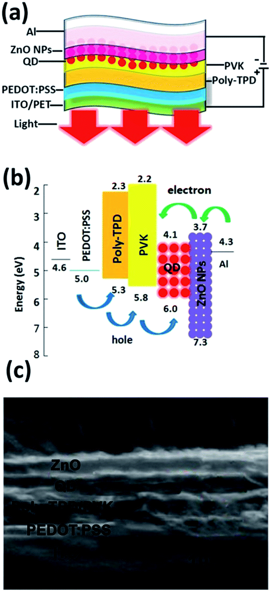 | ||
| Fig. 1 (a) Structure and (b) energy level diagram for the various layers of the QLED, and (c) an SEM image of a cross section of the QLED. | ||
A high-resolution transmission electron microscope (HRTEM) image of the ZnO NPs is displayed in Fig. 2(a) and (b), and the inset shows the statistical distribution graph of the particle size, indicating that the ZnO NPs have an average diameter of ∼2.9 nm. Lattice fringes can be clearly observed in the HRTEM image shown in Fig. 2(b) which suggests the good crystallinity of the ZnO NPs. Fig. 2(c) shows the XRD pattern of the ZnO NPs film. It can be seen in the figure that our synthesized ZnO NPs have a wurtzite structure, which is in good agreement with the literature values (JCPDS card no. 79-0207), although the small particle size led to a significant broadening of the characteristic diffraction pattern. The absorption and photoluminescence spectra of the ZnO NPs are shown in Fig. 2(d). It is observed that the peak position of absorption is located at 320 nm. The band gap Eg of the colloidal ZnO NPs is determined from the intercept between the wavelength axis and the tangent to the linear section of the absorption band edge.19 The band gap is 3.65 eV for the 2.9 nm NPs, which is higher than that of bulk ZnO (3.2–3.3 eV),20 indicating that there is a higher spatial confinement of photo-generated charge carriers in the smaller ZnO particles.21 In the photoluminescence spectra, we observe two peaks. The intensity of one peak is relatively weak and it is located at the fundamental absorption band edge of the NPs. This can be attributed to direct electron–hole recombination.22 The other peak is much more intense and is located at 500–550 nm, reflecting radiative recombination of the electrons and holes, involving traps or structural defects on the surface of the NPs.23
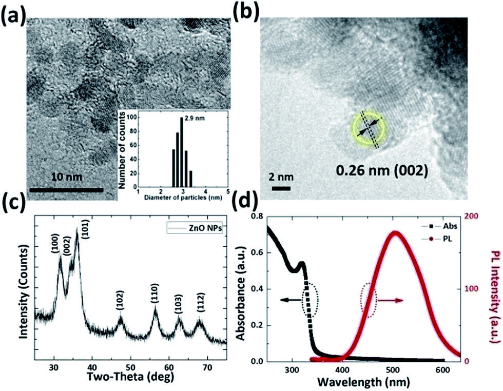 | ||
| Fig. 2 (a) TEM image of ZnO NPs. Inset shows the statistical distribution graph of particle size. (b) HRTEM image of ZnO NPs, (c) XRD pattern from ZnO NPs film, (d) absorption and photoluminescence spectra of ZnO NPs. | ||
Fig. 3(a) and (b) show a comparison of the electrical properties and device performance of QLEDs based on a ZnO NPs ETL and a TiO2 ETL, respectively.
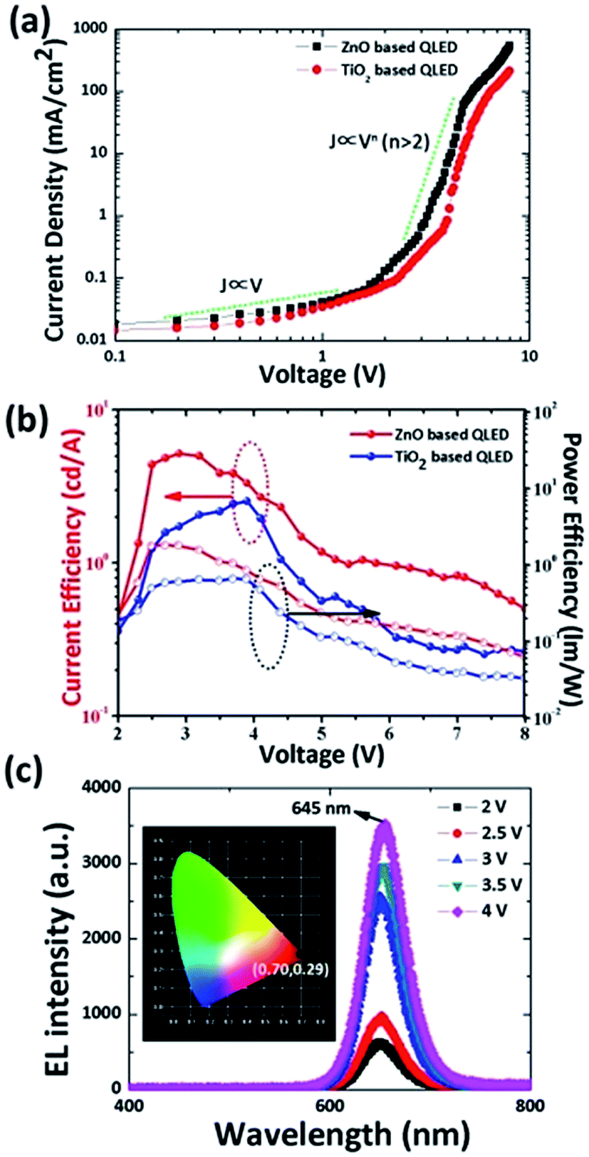 | ||
| Fig. 3 (a) Current density versus voltage characteristics of the QLED, (b) current efficiency and power efficiency of the QLED, (c) EL spectra of the ZnO-based QLED as the applied voltage varies from 2–4 V. Inset shows the CIE coordinate of the device emission. | ||
From Fig. 3(a), it can be seen that the slope of the current density–voltage (J–V) curve shows ohmic behavior (J ∝ V) in the low voltage region for both devices. This changed to present trap-limited conduction (J ∝ Vn, n > 2) as the operating voltage increased. The trap-limited conduction was maintained beyond the turn-on voltage, suggesting that the QDs acted as trap sites in the devices.24
Compared to the TiO2-based QLED, the ZnO-based QLED gives a larger current density over the entire voltage range, so it can be concluded that the ability of electron injection and transport through ZnO NPs is superior to that of TiO2 in our device structure. This is mainly due to the much higher electron mobility of ZnO NPs (4.8 × 10⁻³ cm2 V−1 s−1) (Fig. S5, ESI†) than that of amorphous TiO2 (∼1.0 × 10⁻⁴ cm2 V−1 s−1).25 Meanwhile, the turn-on voltage (driving voltage corresponding to a luminance of 0.1 cd m−2) of the QLED based on ZnO NPs was also significantly decreased to 1.6 V, which was lower than that of the TiO2-based device (2.5 V).
Reduced turn-on driving voltages for the QLED are expected to lead to higher efficiency and better device stability, as Fig. 3(b) shows. The ZnO-based QLED shows higher current and power efficiencies over the entire driving voltage, and the maximum current efficiency and power efficiency are 5.20 cd A−1 and 1.80 lm W−1, respectively, for the ZnO-based QLED and 2.54 cd A−1 and 0.94 lm W−1, respectively, for the TiO2 based QLED. The lowered turn-on voltage and higher efficiency for the ZnO based QLED is attributed to the Auger-assisted charge injection.4 In our system, during this process, the holes can be easily injected into the PVK because of the existence of the poly-TPD, which decreases the energy barrier between the adjacent layers for hole transport and increases the injection force of the holes as shown in Fig. 1(b). These holes accumulate at the PVK/QD interface due to the energy offset (∼0.2 eV) between the HOMO level of PVK and the valence band (VB) edge of the QDs. Similarly, electrons can be easily injected to the QDs because of the large electron mobility of 4.8 × 10⁻³ cm2 V−1 s−1 in ZnO and the small energy barrier of 0.6 eV between the QDs and Al. However, the energy offset of ∼1.9 eV between the LUMO of PVK and the conduction band (CB) of the QDs leads to electron accumulation at the PVK/QD interface. In other words, the injected holes and electrons from the electrodes are likely to accumulate at the interface between the PVK and the QDs due to the large energy barrier offset. Once the Auger assisted hole injection process takes place, where one high energy hole can be obtained after absorbing the energy released from the interfacial recombination of an electron–hole pair,26 the high-energy holes can go over the injection barrier at the PVK/QD interface and recombine with electrons inside the QD layer and emit photons.27 A schematic illustration of the sequence of the Auger-like energy up-conversion process occurring at the heterojunction interface is shown in Fig. S6, ESI.† It is demonstrated that the process is proportional to the electron injection level.18 In other words, the process takes place more easily under the condition of more electron injection from the cathode. Thus, TiO2 based devices do not exhibit a low turn on voltage from Auger-assisted charge injection because of its low electron mobility of 1 × 10⁻⁴ cm2 V−1 s−1.25 In contrast, electrons can be efficiently injected into a ZnO NP-based device at low voltages by the Auger process, which is attributed to the higher electron mobility of 4.8 × 10⁻³ cm2 V−1 s−1 in spite of proper band alignments in both devices. In addition, the good performance of the ZnO-based QLED is also attributed to the design of the poly-TPD/PVK bilayered hole transport structure in the device, which can facilitate hole transport and balance the carrier injection, thus increasing the device performance. Moreover, in order to deeply understand the operating mechanism of different ETL-based devices, we further analyzed the voltage–efficiency characteristics at low operation voltages for the two ETL-based devices. For ZnO based devices, it can be seen that maximum efficiencies can be reached at rather low voltage (less than 3 V), much faster than those of the TiO2-based devices (nearly 4 V). In addition, the results show a rise in current efficiency for the TiO2-based devices as the voltage increases from 2 to 4 V. The rise can be explained by some of the QDs being in an initial (darkened) negatively charged state due to the relatively larger barrier between the HTL and the QDs, and an excess of electrons in the QD region results in QD charging. The amount of hole injection into the QDs layer increases as the voltage increases (current density), which consequently decreases the probability of QD charging and enhances the device efficiency.28 In contrast, Auger assisted energy up conversion hole injection occurs at the PVK/QD interface in the ZnO-based device due to the high electron mobility of the ZnO NPs layer, which leads to an efficient hole injection into the QD layer at low voltage, thus balancing the holes and electrons. As a result, high efficiency can be achieved for the ZnO-based device at a lower current density.
The EL spectrum of the ZnO-based QLED under different voltages is shown in Fig. 3(c). The intensity increases with increasing applied voltage. It can be seen that the position of the EL peak is located at 645 nm. The peak wavelength is red-shifted by 12 nm compared with that of the photoluminescence (PL) peak of the QD solution (Fig. S2, ESI†) stemming from a combination of finite dot-to-dot interactions in the close-packed solid films and the electric-field-induced Stark effect.29 The inset shows that the device emission corresponds to CIE coordinates of (0.70, 0.29).
In order to study the lifetime of the device, luminance versus time for an unencapsulated red QLED under ambient conditions was measured at a constant voltage of 4 V and a current density of 8 mA cm−2, as shown in Fig. 4.
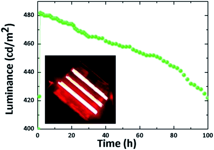 | ||
| Fig. 4 Stability data for an unencapsulated ZnO-based QLED. Inset shows a real photo of the QLED. | ||
The luminance is initially 423 cd m−2 and increases quickly to 482 cd m−2 within a few hours, which is consistent with the trend in previous reports.27,30 Then the luminance intensity decreases very slowly during the next 100 hours. It is easy to find that the lifetime (operating time corresponding to half of the initial luminance) exceeds 100 h. The inset of Fig. 4 shows a photo of the flexible prototype of the ZnO-based QLED under a driving voltage of 4 V. The red emitting light is very dazzling and of high saturation, with corresponding CIE coordinates of (0.70, 0.29). The current ZnO-based QLEDs show considerable stability under ambient conditions, because the ZnO layer not only helps to facilitate the electron transport but also serves as a barrier against the diffusion of oxygen and water molecules into the active layers.
In addition to the good opto-electrical performance, the distinct advantages of our devices are their highly flexible and mechanically robust structure. The QLED can be easily bent into almost any three-dimensional shape with PET substrates, which facilitates the versatile use of our QLED platform. Its robustness is confirmed by bending testing of the devices with the bending radius varying from 3 to 12 mm as shown in Fig. 5. In order to obtain different bending radii of the device, the flexible device is placed against and bent around different curvatures of steel plate, as shown in the inset of Fig. 5. The figure shows that the brightness intensity remains about 75% after being bent 300 times under a bending radius of 3 mm or 4 mm, whereas the brightness changes slightly after being bent 300 times with a bending radius of larger than 4.5 mm.
 | ||
| Fig. 5 Bending testing of the flexible ZnO-based QLED. Inset shows a schematic diagram and corresponding electroluminescence picture of the device with a bending radius of 3 mm after bending 300 times. | ||
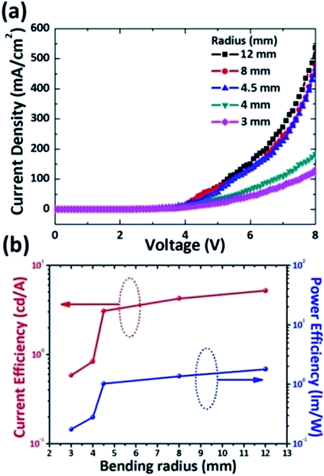
In order to research the performance deterioration of the devices after the bending test and find out the critical bending radius, the current density–voltage and efficiency–voltage characterizations of the device bent into different states of curvature were carried out, and are shown in Fig. 6(a) and (b), respectively.
 | ||
| Fig. 6 (a) Current density versus voltage characteristics of the QLED, (b) maximum current efficiency and power efficiency of the QLED under bending conduction. | ||
It was found that the current density variation trends are similar when the bending radius is larger than 4.5 mm, which is similar to the condition for the device efficiency. Fig. 6(b) shows that the current and power efficiencies both decrease quickly once the bending radius is smaller than 4.5 mm, which suggests that the critical radius is 4.5 mm. The poor performance of the device under small bending radius conduction is attributed to the onset of the cracking phenomenon in the ITO films, because the molecular components in the LED device are highly compressible.31Table 1 summarizes the detailed performance parameters of the QLEDs of different bending radii in the present study. The small critical bending radius suggests that the flexible QLED has broad potential in the application of large, conformable, or roll-up flat panel displays. In addition, flexible QLED-based displays have advantages in fabricating cost because they can be mass manufactured on a roll-to-roll basis owing to the good flexibility of the QLED.
| Bending radius (mm) | Luminance loss (%) | C-D (mA cm−2) | η P (lm W−1) | η A (cd A−1) |
|---|---|---|---|---|
| 3 | 24.3 | 44.53 | 0.18 | 0.59 |
| 4 | 22.9 | 67.15 | 0.28 | 0.84 |
| 4.5 | 12.1 | 133.40 | 1.03 | 3.09 |
| 8 | 9.2 | 134.02 | 1.37 | 4.26 |
| 12 | 8.5 | 142.27 | 1.67 | 5.09 |
4. Conclusions
In summary, we designed and fabricated flexible red-emitting QLEDs on ITO/PET substrates using ZnO NPs as an ETL, which display a low turn on voltage of 1.60 V and high current and power efficiencies of 5.20 cd A−1 and 1.80 lm W−1, respectively. The superior performance is a result of the higher electron mobility of ZnO NPs and more suitable energy level of the bilayered HTL consisting of poly-TPD/PVK. Moreover, a lifetime of more than 100 h for the unencapsulated flexible device under ambient conditions has been achieved. Finally, the flexible QLEDs exhibit a critical bending radius down to 4.5 mm, which is useful for their applications in flexible displays and roll to roll manufacture. Our work paves the way for realizing all solution processed flexible QLEDs and presents the broad potential of flexible QD optoelectronics.Acknowledgements
This work was supported partially by the National Key Basic Research Program 973 (2013CB328804, 2013CB328803), the National High-Tech R&D Program 863 of China (2012AA03A302, 2013AA011004), National Natural Science Foundation Project (51120125001, 61271053, 61306140, 61405033, 91333118, 61372030, 61307077 and 51202028), Natural Science Foundation Project of Jiangsu Province (BK20141390, BK20130629, and BK20130618), Beijing Natural Science Foundation (4144076) and China Postdoctoral Science Foundation (2013M530613 and 2015T80080).Notes and references
- Y. Shirasaki, G. J. Supran, M. G. Bawendi and V. Bulovic, Nat. Photonics, 2013, 7, 13–23 CrossRef CAS PubMed
.
- Q. Sun, Y. A. Wang, L. S. Li, D. Wang, T. Zhu, J. Xu, C. Yang and Y. Li, Nat. Photonics, 2007, 1, 717–722 CrossRef CAS PubMed
- V. L. Colvin, M. C. Schlamp and A. P. Alivisatos, Nature, 1994, 370, 354–357 CrossRef CAS PubMed
- L. Qian, Y. Zheng, J. G. Xue and P. H. Holloway, Nat. Photonics, 2011, 5, 543–548 CrossRef CAS PubMed
- Y. Shirasaki, G. J. Supran, M. G. Bawendi and V. Bulović, Nat. Photonics, 2013, 7, 13–23 CrossRef CAS PubMed
- X. Dai, Z. Zhang, Y. Jin, Y. Niu, H. Cao, X. Liang, L. Chen, J. Wang and X. Peng, Nature, 2014, 515, 96–99 CrossRef CAS PubMed
- X. Y. Yang, E. Mutlugun, C. Dang, K. Dev, Y. Gao, S. T. Tan, X. W. Sun and H. V. Demir, ACS Nano, 2014, 8, 8224–8231 CrossRef CAS PubMed
- S. Reineke, Nat. Mater., 2015, 14, 459–462 CrossRef CAS PubMed
- Y. Yang, Y. Zheng, W. Cao, A. Titov, J. Hyvonen, R. MandersJesse, J. Xue, P. H. Holloway and L. Qian, Nat. Photonics, 2015, 9, 259–266 CrossRef CAS PubMed
- N. Y. Kim, S. H. Hong, J. W. Kang, N. Myoung, S. Y. Yim, S. Jung, K. Lee, C. W. Tu and S. J. Park, RSC Adv., 2015, 5(25), 19624–19629 RSC
- J. Kwak, W. K. Bae, D. Lee, I. Park, J. Lim, M. Park, H. Cho, H. Woo, D. Y. Yoon, K. Char, S. Lee and C. Lee, Nano Lett., 2012, 12, 2362–2366 CrossRef CAS PubMed
- J. Lim, W. K. Bae, D. Lee, M. K. Nam, J. Jung, C. Lee, K. Char and S. Lee, Chem. Mater., 2011, 23, 4459–4463 CrossRef CAS
- Z. N. Tan, J. Xu, C. F. Zhang, T. Zhu, F. Zhang, B. Hedrick, S. Pickering, J. Wu, H. P. Su, S. Gao, A. Y. Wang, B. Kimball, J. Ruzyllo, N. S. Dellas and S. E. Mohney, J. Appl. Phys., 2009, 105(3), 034312 CrossRef PubMed
- R. Z. Liang, D. P. Yan, R. Tian, X. J. Yu, W. Y. Shi, C. Y. Li, M. Wei, D. G. Evans and X. Duan, Chem. Mater., 2014, 26, 2595–2600 CrossRef CAS
- M. J. Panzer, V. Wood, S. M. Geyer, M. G. Bawendi and V. Bulovic, J. Disp. Technol., 2010, 6, 90–93 CrossRef CAS
- Y. Kim, T. Greco, C. Ippen, A. Wedel, M. S. Oh, C. J. Han and J. Kim, Nanosci. Nanotechnol. Lett., 2013, 5, 1065–1069 CrossRef CAS PubMed
- W. K. Bae, K. Char, H. Hur and S. Lee, Chem. Mater., 2008, 20, 531–539 CrossRef CAS
- L. Qian, Y. Zheng, K. R. Choudhury, D. Bera, F. So, J. G. Xue and P. H. Holloway, Nano Today, 2010, 5, 384–389 CrossRef CAS PubMed
- Y. V. Panasiuk, O. E. Raevskaya, O. L. Stroyuk, S. Y. Kuchmiy, V. M. Dzhagan, M. Hietschold and D. R. T. Zahn, Nanotechnology, 2014, 25, 075601 CrossRef CAS PubMed
- U. Ozgur, Y. I. Alivov, C. Liu, A. Teke, M. A. Reshchikov, S. Dogan, V. Avrutin, S. J. Cho and H. Morkoc, J. Appl. Phys., 2005, 98, 041301 CrossRef PubMed
- P. V. Kamat and B. Patrick, J. Phys. Chem., 1992, 96, 6829–6834 CrossRef CAS
- O. L. Stroyuk, V. M. Dzhagan, V. V. Shvalagin and S. Y. Kuchmiy, J. Phys. Chem. C, 2010, 114, 220–225 CAS
- L. Spanhel and M. A. Anderson, J. Am. Chem. Soc., 1991, 113, 2826–2833 CrossRef CAS
- R. Hikmet, D. Talapin and H. Weller, J. Appl. Phys., 2003, 93, 3509–3514 CrossRef CAS PubMed
- J. Y. Kim, S. H. Kim, H. H. Lee, K. Lee, W. L. Ma, X. Gong and A. J. Heeger, Adv. Mater., 2006, 18, 572–576 CrossRef CAS PubMed
- H. V. Demir, S. Nizamoglu, T. Erdem, E. Mutlugun, N. Gaponik and A. Eychmuller, Nano Today, 2011, 6(6), 632–647 CrossRef CAS PubMed
- K. Qasim, J. Chen, Z. Li, W. Lei and J. Xa, RSC Adv., 2013, 3, 12104–12108 RSC
- W. Xu, W. Y. Ji, P. T. Jing, X. Yuan, Y. A. Wang, W. D. Xiang and J. L. Zhao, Opt. Lett., 2014, 39, 426–429 CrossRef CAS PubMed
- H. H. Kim, S. Park, Y. Yi, D. I. Son, C. Park, D. K. Hwang and W. K. Choi, Sci. Rep., 2015, 5, 5 Search PubMed
- J. Chen, D. Zhao, C. Li, F. Xu, W. Lei, L. Sun, A. Nathan and X. W. Sun, Sci. Rep., 2014, 4, 4085 Search PubMed
- G. Gu, P. Burrows, S. Venkatesh, S. Forrest and M. Thompson, Opt. Lett., 1997, 22, 172–174 CrossRef CAS
Footnote |
| † Electronic supplementary information (ESI) available: Optimized procedure of the QLED fabrication, characteristics of the QDs, characteristics of the ZnO NP film, illustration of the Auger-like energy up-conversion process, UPS measurements, UV-Vis absorption spectrum for the ZnO film, TFT characteristics of the ZnO nanoparticle film. See DOI: 10.1039/c5ra10656g |
| This journal is © The Royal Society of Chemistry 2015 |