DOI:
10.1039/C5RA09824F
(Paper)
RSC Adv., 2015,
5, 55186-55190
First principles study of the electronic properties of a Ni3(2,3,6,7,10,11-hexaaminotriphenylene)2 monolayer under biaxial strain
Received
25th May 2015
, Accepted 12th June 2015
First published on 12th June 2015
Abstract
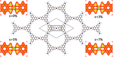
Applying first principles calculations, the electronic structure of a Ni3(HITP)2 (HITP = 2,3,6,7,10,11-hexaaminotriphenylene) monolayer have been investigated with both GGA and GGA + U methods. The Ni3(HITP)2 monolayer is semi-conductive with a narrow indirect band in an unstrained system. Under biaxial strain, our computation results reveal that the monolayer becomes metallic after the band gap gradually decreases to zero with increased strain. The 2D sheet is verified to have typical π-conjugated characteristics with each Ni atom adopting the dsp2 hybridization at zero strain. We demonstrate the variation of the charge density of the monolayer to show the gradual weakening of the Ni–N bond as the strain increases. Our band structure and charge density analysis indicate the variation of the band gap can be the result of charge redistribution between the Ni and N atoms due to the biaxial strain applied.
1. Introduction
Monolayer nanosheet materials have changed our knowledge of material science since the mechanical exfoliation of graphene by Novoselov and Geim.1 Many great efforts have been made to extend the research on their physical and chemical properties derived from their two-dimensional (2D) nature. For example, graphene is one of the most prominent nanosheet materials with in-plane pi-conjugation,1 which has an extremely high electron mobility due to the linear dispersion relation in its band structure around the Dirac point.2 However, the disadvantage of graphene is its poor application in semiconductor-based devices due to its zero bandgap.3–5 Since modification of graphene cannot perfectly solve this problem,6,7 researchers started to focus on investigating other types of 2D nanosheet materials which exhibit similar electronic properties without a zero band gap, such as hexagonal BN sheets,8 transition metal dichalcogenides,9,10 silicone,11 germanane12 and metal organic frameworks.13–15
With the advances in synthesis and experimental techniques, “top-down” and “bottom-up” are the most effective methods when the graphene analogues are considered.16–19 Recently some of the “bottom-up” solution-based synthetic methods have shown that many sophisticated ligands bridging certain metal ions exhibit non-zero bandgaps and considerable electrical conductivity in the 2D plane.20 Therefore, these 2D metal–organic networks described as semiconducting metal–organic graphene analogues (s-MOGs) seem to be promising for future electronic applications.
Inspired by the success of dithiolene-based s-MOGs, a new crystalline s-MOG with very high electrical conductivity called Ni3(HITP)2 (HITP = 2,3,6,7,10,11-hexaaminotriphenylene) was synthesized and analysed as bulk powders and thin films.20 Although the electronic properties of the 3D Ni3(HITP)2 bulk samples were found to be metallic recently, the monolayer framework turned out to be semi-conductive,21 which made us wonder if there exists some methods to modify its band gap so that we could trigger some more interesting properties.
Instead of other various methods such as nanostructuring,22,23 doping,24 chemical functionalization,25 the application of an external electric field,26,27 and substrate absorption to break the symmetry,28 the application of strain became our choice. A controlled introduction of biaxial strain provides a convenient and reversible way to investigate both the tuning of the electronic structure and mechanical properties at the same time, so that we are able to find out the connection between the band gap and the biaxial strain.
In this work, we investigate the basic geometric and electronic properties of a 2D Ni3(HITP)2 monolayer through its band structure. We also simulate the changes of the cell structure and electronic structure when to the monolayer is applied increasing isotropic biaxial strain. In the end, we investigate the mechanism of how the biaxial strain effects the electronic structure.
2. Computational details
Geometry optimizations were performed using the Vienna ab initio simulation package (VASP).29,30 The exchange–correlation energy was described using the generalized gradient approximation (GGA) in the form of Perdew, Burke, and Ernzerhof (PBE).31 The electron–ion interactions were described using the projector augmented wave (PAW) method with an energy cutoff of 400 eV (the convergence criteria was 0.01 eV), which is primarily a frozen-core all-electron calculation.32 Spin-polarized GGA + U calculations were also performed with a Ueff value of 3 eV for the Ni ions, since DFT often provides an unsatisfactory description for a strongly correlated transition-metal system with localized d subshells, which have been tested and used in previous theoretical studies.33 We also checked the band structure with a Ueff value of 4 eV and 5 eV to check the best value of Ueff. We applied the 2D periodic boundary conditions with the unit cell forced into P6/mmm symmetry, and a vacuum space of 15 Å along the z direction was adopted to avoid interactions between two layers in nearest-neighbouring unit cells. For the structure optimization, the atoms were relaxed in the direction of the Hellmann–Feynman force using the conjugate gradient method until a stringent convergence criterion (= 0.03 eV Å−1) was satisfied. Since our model was based on 2D Ni3(HITP)2 nanosheets, the Brillouin zone was represented by a Monkhorst–Pack k-point mesh of 3 × 3 × 1 for geometry optimizations (the convergence criteria was 0.001 eV), and a large grid (9 × 9 × 1) was used for self-consistent calculations. The 3D bulk structure was also briefly calculated to be compared with the geometry structure of 2D nanosheet. The Monkhorst–Pack k-point mesh for geometry optimizations was set to be 2 × 2 × 6. The periodic 2D framework and 3D bulk structure were constructed following the consideration of previous work.20,21
3. Results and discussion
3.1 2D Ni3(HITP)2 nanosheet and 3D bulk structure
To begin, we compared the geometric properties of a strain-free monolayer nanosheet of Ni3(HITP)2 with its bulk structure. The lattice parameter of the Ni3(HITP)2 unit cell was optimized to be 21.96 Å, which is slightly bigger than the 21.78 Å in the bulk structure. We also identified that the Ni3(HITP)2 monolayer is a porous material with a very large pore size of 19.695 Å (N–N)∼20.633 Å (C–C) as shown in Fig. 1, and the Ni–N bond length (LNi–N) and N–C bond length (LN–C) are 1.838 Å and 1.357 Å, respectively. While in the bulk structure, the pore size is 19.655 Å (N–N)∼20.452 Å (C–C) and the LNi–N and LN–C are 1.820 Å and 1.358 Å, respectively. The comparison of the 2D and 3D structures of Ni3(HITP)2 indicates that the single layers of the bulk are constrained since the 2D parameters are slightly larger than 3D parameters.
 |
| Fig. 1 Optimized structure of the 2D Ni3(HITP)2 monolayer. The atoms of the unit cell are forced into P6/mmm symmetry represented by the dashed rhombus. H atoms are used to terminate the edges. | |
Consistent with the work of Chen et al.21 Fig. 2 depicts that the monolayer Ni3(HITP)2 framework is predicted to be a semiconductor with an indirect band gap of 0.118 eV at the GGA level, slightly less than the 0.128 eV at the GGA + U level (Ueff = 3 eV) due to that the valance band maximum (VBM) decreases. As we increase the value of Ueff to 4 eV and 5 eV, the band gap increases to nearly 0.14 eV. Compared with ref. 21, we believe Ueff = 3 eV is the most appropriate value for these calculations. This narrow band gap is much smaller than in traditional semiconductors.
 |
| Fig. 2 Computed band structures using the GGA (a) and GGA + U (b) method. The Fermi level is marked by a thin purple line, while the blue and red lines are used to show the change of the conduction band minimum (CBM) and valance band maximum (VBM), respectively. | |
3.2 Biaxial strain applied to the Ni3(HITP)2 monolayer
We choose to apply increasing biaxial tensile strain in plane which is defined by the relation ε = (a − a0)/a0 × 100, where a and a0 are the lattice parameters of the strained and unstrained systems, respectively. In order to have a good understanding of the process, Δε is set to 1%. The strain energy of each step is defined by the relation Es = Eε − E0, where Eε is the total energy of the strained unit cell and E0 is the corresponding energy at equilibrium.
Fig. 3 shows that the tuning of the electronic structure has been achieved as we expected. Though there is no change of the nonmagnetic properties, the electronic properties are slowly affected by the magnitude of the applied strain. We find it interesting that the band gap decreases with the strain and become zero when ε is 7% in Fig. 3(d). Fig. 3 also demonstrates that the electronic properties of the 2D sheet change from semi-conductive to metallic due to that its highest occupied valance band (HOVB) increases and its lowest unoccupied conduction band (LUCB) decreases. The HOVB at the K point increases from −0.0582 eV to 0 eV and the LUCB at the Γ point decreases from 0.0696 eV to −0.0228 eV. The band gap vanishes due to that the value of HOVB becomes higher than the value of LUCB at ε = 7%.
 |
| Fig. 3 Electronic band structures of the 2D Ni3(HITP)2 monolayer at ε = 1% (a), 3% (b), 5% (c) and 7% (d). | |
Recent research showed that the delocalized d orbitals of Ni atoms provide contributions to both the HOVB and LUCB,21 indicating that the Ni–N bonds play a key part in the band gap variation as a function of the biaxial strain. Fig. 4(a) and (b) present the computed DOS and PDOS of the 2D Ni3(HITP)2 monolayer at ε = 0 and ε = 7%, respectively. Both of them show that the band around the Fermi level is mostly contributed by Ni-d, C-p and N-p orbitals. In Fig. 4(a), the density of states at the HOVB and LUCB at ε = 0 are zero, while in Fig. 4(b), the density of states at the same positions increase to 0.44 and 1.18 states per eV. The unoccupied Fermi level at ε = 0 becomes occupied at ε = 7%, which indicates that the changes of the band structure are mainly caused by the change of occupation at the Fermi level.
 |
| Fig. 4 The DOS and PDOS of the 2D Ni3(HITP)2 monolayer at ε = 0 (a) and ε = 7% (b). Black, red and dark blue lines represent the s, p and d orbitals of the different atoms. The LUCB and HOVB at ε = 0 are marked by light blue and green lines. | |
In order to understand the changes of the PDOS at the Fermi level, we focus on the bond lengths of the Ni, N and C atoms as well as their charge density distribution. The 2D monolayer remains metallic when ε ≥ 7%. As the strain is increased, LNi–N and LN–C change as shown in Fig. 5(b). It is obvious that LNi–N abruptly increases at ε = 9% while LN–C decreases, and in Fig. 5(a) the slope of Es suddenly changes at ε = 8%, which indicates that ε = 8% corresponds to the maximal biaxial strain before fragmentation.
 |
| Fig. 5 The strain energy (Es) of each step (a) and the Ni–N (black), N–C (red) bond lengths (b) of the Ni3(HITP)2 monolayer as a function of the biaxial strain. | |
Fig. 6(a) verifies that the 2D sheet exhibits typical π-conjugated characteristics with each Ni atom adopting dsp2 hybridization, which is in good agreement with the earlier result.21 Fig. 6(b)–(d) demonstrate the gradual redistribution of charge density as the strain increases. The increase of the Ni–N bond length induces the charge density to redistribute more closely to Ni and N respectively, so that the weakening of the Ni–N bond will be compensated. The extra charge that Ni and N get will occupy more energy levels which affects the bottom of the HOVB and the top of the LUCB as the band gap decreases and the Fermi level becomes occupied.
 |
| Fig. 6 Charge density isosurfaces of the Ni3(HITP)2 monolayer at ε = 0 (a), 3% (b), 5% (c) and 7% (d). The variation of colour from green to yellow to red represents a decreasing level of charge density value. The isosurface value for the charge density is 0.08 e per Bohr3. | |
4. Conclusions
In this study, we investigated the electronic structure of a 2D Ni3(HITP)2 monolayer under biaxial strain. We compared the electronic structure of the monolayer using GGA and GGA + U methods at zero strain. The 2D sheet is semi-conductive with a narrow indirect band gap of 0.128 eV when the system is in equilibrium. Under biaxial strain, our computation results revealed that the band gap of the monolayer gradually decreased with increased strain and became zero at ε = 7%. Our DOS and PDOS analysis showed that the unoccupied Fermi level at ε = 0 becomes occupied at ε = 7%, which indicates that the band structure changes are mainly caused by occupation changes at the Fermi level. The monolayer turned into fragments at ε = 9% as the Ni–N bond length abruptly increased and the N–C bond length decreased. At the end, we presented the variation of charge density of the monolayer. The 2D sheet was verified to have typical π-conjugated characteristics with each Ni atom adopting the dsp2 hybridization at ε = 0. The charge density variation also showed the gradual weakening of the Ni–N bond as the strain increased. The band structure and charge density analysis indicated that the variation of the band gap could be ascribed to charge redistribution between the Ni and N atoms due to the biaxial strain applied. Our work is just a small exploration of this new material. There are so many potential properties to be discovered. This interesting property may inspire development of some other future application or experimental phenomenon. We hope our research will motivate more experimental and theoretical studies on this newly developed material and its possible applications in nanoelectronics.
Acknowledgements
Our work was supported by the National Natural Science Foundation of China (NNSFC) (grant no. 51474176, 51174168, 51274167), the Natural Science Basic Research Plan in Shaanxi Province of China (grant no. 2014JM7261), the Specialized Research Fund for the Doctoral Program of Higher Education of China (20136102120021), and the Fundamental Research Funds for the Central Universities (3102014JCQ01024).
References
- K. S. Novoselov, A. K. Geim, S. V. Morozov, D. Jiang, Y. Zhang, S. V. Dubonos, I. V. Grigorieva and A. A. Firsov, Science, 2004, 306, 666 CrossRef CAS PubMed.
- A. K. Geim and K. S. Novoselov, Nat. Mater., 2007, 6, 183 CrossRef CAS PubMed.
- K. S. Novoselov, A. K. Geim, S. V. Morozov, D. Jiang, M. I. Katsnelson, I. V. Grigorieva, S. V. Dubonos and A. A. Firsov, Nature, 2005, 438, 197 CrossRef CAS PubMed.
- A. H. Castro Neto, F. Guinea, N. M. R. Peres, K. S. Novoselov and A. K. Geim, Rev. Mod. Phys., 2009, 81, 109 CrossRef CAS.
- P. Avouris, Nano Lett., 2010, 10, 4285 CrossRef CAS PubMed.
- P. Ruffieux, J. Cai, N. C. Plumb, L. Patthey, D. Prezzi, A. Ferretti, E. Molinari, X. Feng, K. Müllen, C. A. Pignedoli and R. Fasel, ACS Nano, 2012, 6, 6930 CrossRef CAS PubMed.
- V. Georgakilas, M. Otyepka, A. B. Bourlinos, V. Chandra, N. Kim, K. C. Kemp, P. Hobza, R. Zboril and K. S. Kim, Chem. Rev., 2012, 112, 6156 CrossRef CAS PubMed.
- Y. Kubota, K. Watanabe, O. Tsuda and T. Taniguchi, Science, 2007, 317, 932 CrossRef CAS PubMed.
- J. N. Coleman, M. Lotya, A. O’Neill, S. D. Bergin, P. J. King, U. Khan, K. Young, A. Gaucher, S. De, R. J. Smith, I. V. Shvets, S. K. Arora, G. Stanton, H.-Y. Kim, K. Lee, G. T. Kim, G. S. Duesberg, T. Hallam, J. J. Boland, J. J. Wang, J. F. Donegan, J. C. Grunlan, G. Moriarty, A. Shmeliov, R. J. Nicholls, J. M. Perkins, E. M. Grieveson, K. Theuwissen, D. W. McComb, P. D. Nellist and V. Nicolosi, Science, 2011, 331, 568 CrossRef CAS PubMed.
- A. Splendiani, L. Sun, Y. Zhang, T. Li, J. Kim, C.-Y. Chim, G. Galli and F. Wang, Nano Lett., 2010, 10, 1271 CrossRef CAS PubMed.
- B. Lalmi, H. Oughaddou, H. Enriquez, A. Kara, S. Vizzini, B. Ealet and B. Aufray, Appl. Phys. Lett., 2010, 97, 223109 CrossRef PubMed.
- E. Bianco, S. Butler, S. Jiang, O. D. Restrepo, W. Windl and J. E. Goldberger, ACS Nano, 2013, 7, 4414 CrossRef CAS PubMed.
- T. Kambe, R. Sakamoto, K. Hoshiko, K. Takada, M. Miyachi, J.-H. Ryu, S. Sasaki, J. Kim, K. Nakazato, M. Takata and H. Nishihara, J. Am. Chem. Soc., 2013, 135, 2462 CrossRef CAS PubMed.
- N. Abdurakhmanova, T.-C. Tseng, A. Langner, C. S. Kley, V. Sessi, S. Stepanow and K. Kern, Phys. Rev. Lett., 2013, 110, 027202 CrossRef CAS.
- M. Abel, S. Clair, O. Ourdjini, M. Mossoyan and L. Porte, J. Am. Chem. Soc., 2010, 133, 1203 CrossRef PubMed.
- K. F. Mak, C. Lee, J. Hone, J. Shan and T. F. Heinz, Phys. Rev. Lett., 2010, 105, 136805 CrossRef.
- M. Chhowalla, H. S. Shin, G. Eda, L.-J. Li, K. P. Loh and H. Zhang, Nat. Chem., 2013, 5, 263 CrossRef PubMed.
- R. Gutzler and D. F. Perepichka, J. Am. Chem. Soc., 2013, 135, 16585 CrossRef CAS PubMed.
- J. W. Colson and W. R. Dichtel, Nat. Chem., 2013, 5, 453 CrossRef CAS PubMed.
- D. Sheberla, L. Sun, M. A. Blood-Forsythe, S. Er, C. R. Wade, C. K. Brozek, A. N. Aspuru-Guzik and M. Dincă, J. Am. Chem. Soc., 2014, 136, 8859 CrossRef CAS PubMed.
- S. Chen, J. Dai and X. C. Zeng, Phys. Chem. Chem. Phys., 2015, 17, 5954–5958 RSC.
- X. Li, X. Wang, L. Zhang, S. Lee and H. Dai, Science, 2008, 319, 1229 CrossRef CAS PubMed.
- M. Y. Han, B. Özylmaz, Y. Zhang and P. Kim, Phys. Rev. Lett., 2007, 98, 206805 CrossRef.
- Y. Gong, Z. Liu, A. R. Lupini, G. Shi, J. Lin, S. Najmaei, Z. Lin, A. L. Elías, A. Berkdemir, G. You, H. Terrones, M. Terrones, R. Vajtai, S. T. Pantelides, S. J. Pennycook, J. Lou, W. Zhou and P. M. Ajayan, Nano Lett., 2014, 14, 442 CrossRef CAS PubMed.
- R. Balog, B. Jørgensen, L. Nilsson, M. Andersen, E. Rienks, M. Bianchi, M. Fanetti, E. Lægsgaard, A. Baraldi, S. Lizzit, Z. Sljivancanin, F. Besenbacher, B. Hammer, T. G. Pedersen, P. Hofmann and L. Hornekær, Nat. Mater., 2010, 9, 315 CrossRef CAS PubMed.
- Y. Li and Z. Chen, J. Phys. Chem. C, 2014, 118, 1148 CAS.
- A. Klien, S. Tiefenbacher, V. Eyert, C. Pettenkofer and W. Jaegermann, Phys. Rev. B: Condens. Matter Mater. Phys., 2001, 64, 205416 CrossRef.
- S. Y. Zhou, G.-H. Gweon, A. V. Fedorov, P. N. First, W. A. DeHeer, D.-H. Lee, F. Guinea, A. H. Castro Neto and A. Lanzara, Nat. Mater., 2007, 6, 770 CrossRef CAS PubMed.
- G. Kresse and J. Hafner, Phys. Rev. B: Condens. Matter Mater. Phys., 1993, 47, 558 CrossRef CAS.
- G. Kresse and D. Joubert, Phys. Rev. B: Condens. Matter Mater. Phys., 1999, 59, 1758 CrossRef CAS.
- J. P. Perdew, K. Burke and M. Ernzerhof, Phys. Rev. Lett., 1996, 77, 3865 CrossRef CAS.
- G. Kresse and J. Furthmüller, Phys. Rev. B: Condens. Matter Mater. Phys., 1996, 54, 11169 CrossRef CAS.
- J. Zhou and Q. Sun, J. Am. Chem. Soc., 2011, 133, 15113 CrossRef CAS PubMed.
|
This journal is © The Royal Society of Chemistry 2015 |
Click here to see how this site uses Cookies. View our privacy policy here.