Direct imprinting of thermally reduced silver nanoparticles via deformation-driven ink injection for high-performance, flexible metal grid embedded transparent conductors

Y. S. Oh, D. Y. Choi and H. J. Sung*
Department of Mechanical Engineering, KAIST, 291 Daehak-ro, Yuseong-gu, Daejeon 34141, Korea. E-mail: hjsung@kaist.ac.kr

Received 20th May 2015 , Accepted 20th July 2015

First published on 22nd July 2015


Abstract

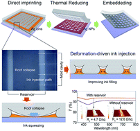
We developed a method for direct imprinting of thermally reduced Ag nanoparticles via deformation-driven ink injection to yield high-performance metal grid transparent conductors (TCs). A grid patterned mold was created to have a macroscale cavity by designing a “reservoir” that captured outgoing ink and injected the captured ink into the grid patterned mold cavity by a roof deformation. The ink supply from the reservoir contributed to not only improving the ink filling, but also decreasing the linewidth of the grid patterned mold cavity due to a sidewall deformation on the liquid film. The metal grid TCs fabricated using the reservoir-assisted mold performed better than the metal grids prepared using the typical mold in terms of the sheet resistance (4.7 vs. 12.6 Ω sq−1) and transmittance at 550 nm (93.5 vs. 90.7%), respectively. The metal grid TCs were embedded into large-scale, flexible, and transparent films, which showed a reasonable electromechanical stability under repeated bending. The metal grid embedded TCs were fabricated for application in touch screen panels. Our approach provides a new route for fabrication of high-performance, solution-processed micro/nanoscale metal grid TCs and hybrid TCs based on Ag nanowires, graphene, or carbon nanotubes for use in a variety of next-generation flexible optoelectronic devices.


1. Introduction

Transparent conductors (TCs) are key components of various optoelectronic devices, such as photovoltaic cells,1 organic light-emitting diodes,2 or touch screen panels.3 Conventionally, indium tin oxide (ITO) is the most widely used as a transparent conductive material due to its low sheet resistance and excellent optical transparency; however, the inherent deficiencies of ITO hinder applications in flexible optoelectronic devices.4 Although there have been increasing efforts in developing alternative materials of TCs, including conductive polymers,5 graphene6,7 and carbon nanotubes,8,9 their performance is insufficient for the optoelectronic applications in terms of conductivity and stability. Also, metal-based TCs such as random metal nanowire networks and regular metal grids have been found to provide superior electrical and optical properties, comparable to ITO. Silver nanowire networks, in particular, have been explored for their utility in flexible optoelectronic devices due to low fabrication costs, good flexibility, high conductivity and transmittance.10–12 However, they suffer from the difficulty of uniform distribution on a substrate, the easy detachment by mechanical stress, and the inferior electrical contacts between nanowires. Also, the metal networks fabricated by electrospining process of polymers and metal evaporation show a good performance, but they are required for expensive vacuum process and etching process.13 The metal grid TCs have advantages of easy handling of sheet resistance and optical transmittance by varying the grid width, spacing, and thickness as well as low junction resistance.14 They are classified into nanoscale metal grids fabricated by a combination of nanoimprinting and transfer printing, and microscale metal grids fabricated by hot embossing, inkjet printing and self-assembly.15–22

Polydimethylsiloxane (PDMS)-based patterning methods, which are often referred to as “soft lithography”, can directly produce micro/nanoscale patternings of functional materials such as nanoparticle (NP) and polymer at low cost and high throughput.23–27 Among the PDMS-based patterning methods, a direct imprinting of colloidal metal NPs has tremendous potential for fabricating metal-based micro/nanoscale structures due to several advantages of a PDMS mold such as the minimum residual layers by conformal contact, the ease of demolding by low surface energy and the degassing by high gas permeability.28–30 However, there are two challenges to fabricate high-performance metal-based TCs using the direct imprinting of colloidal metal NPs. Firstly, colloidal metal NPs during the direct imprinting process suffers from NP agglomerates and low metal concentration. The instability of colloidal metal NPs can generate the unwanted residual layers. After solvent evaporation, metal structures, of which size is smaller than that of a mold cavity, are formed due to low metal concentration. As an alternative of the colloidal metal NPs, an Ag ion ink has distinguishing advantages, including lower sintering temperature (less than 150 °C), higher metal content and less aggregation.31,32 The Ag ion ink has been generally used in macroscale (>50 μm) electronics on the flexible substrate. Perelaer et al.33 suggested inkjet-printed Ag ions of which electric conductivity was obtained on the flexible substrate after thermally reducing and sintering at low temperature. However, the inkjet-printed patterns had low resolution (>100 μm), low throughput and non-uniformity induced by coffee-stain effect. Kim et al.34 proposed micro transfer printing of Ag ion ink, which was difficult to fabricate scalable, uniform and high conductive patterns due to a transferring of liquid ink. To the best of our knowledge, the metal grid TCs fabricated by direct imprinting via thermally reduction of Ag ions have not yet been demonstrated. Secondly, a sufficient filling of the concentrated ink inside the mold cavity should be achieved with the minimum residual layers. The ink filling and the residual layers are considerably affected by a liquid film between the mold and the substrate due to the mold geometry and fluid properties (viscosity and surface tension). The high density mold cavity can induce the insufficient ink filling due to a lack of liquid film, while the low density mold cavity can generate the unwanted residual layers. Also, the fluid properties are controlled by the solvent exchange (e.g. α-terpineol).28 However, the Ag ion ink is difficult to replace the carrier solvent due to thermal and chemical instability of Ag ions. In addition, the volume reduction of the mold cavity by the applied pressure and the trapped air inside the mold cavity lower the ink filling.

The next-generation flexible metal-based TCs are essentially required for not only the high-performance (a sheet resistance of 10 Ω sq−1 and a transmittance of 90%), but also the electromechanical stability. Also, as the performance in flexible optoelectronic devices is highly dependent on the surface topography, the surface roughness should be reduced.11 The embedding process is allowed to reduce the surface roughness and protect the TCs from a mechanical and physical stress. Recently, Ag nanowire-embedded TCs have been reported using thermal-curable polymers like the PDMS35 and an UV-curable polymer like the Norland Optical Adhesive (NOA).36 Also, the metal grid embedded TCs using the gravure printing method were fabricated, but they showed a limited use in the optoelectronic devices due to the low resolution (>40 μm).22

Herein, we present a method for direct imprinting of thermally reduced Ag NPs using a reservoir-assisted mold in order to fabricate the high-performance metal grid TCs. A grid patterned mold cavity (microscale cavity) was incorporated with the macroscale cavity, i.e., the reservoir which functioned as a capture of an outgoing ink, an injection of the captured ink to the grid patterned mold cavity by a roof deformation. The ink injection from the reservoir contributed to not only improving the ink filling in the mold cavity, but also reducing the linewidth of the grid patterned mold cavity due to a sidewall deformation on the liquid film. These behaviors not only lowered the sheet resistance (Rs), but also enhanced the transmittance (T) at the same time. The metal grid TCs fabricated using the reservoir-assisted mold (R-mold) yielded better sheet resistance and transmittance values: Rs = 4.7 and 12.6 Ω sq−1 and T550 nm = 93.5 and 90.7%, respectively, compared to the metal grids produced using the typical mold without a reservoir (T-mold). The high-performance metal grid TCs were embedded into a polymer matrix, NOA 81, which exhibited a reasonable electromechanical stability and a smooth surface. The metal grid embedded TCs were fabricated for application to touch screen panels. This results constitute an important step toward high-performance, solution-processed, flexible, embedded micro/nanoscale metal grid TCs.

2. Experimental

2.1 Reduction of Ag ions

The Ag ion ink (TEC-IJ-060, Inktec), which has a viscosity (0.005–0.015 Pa s), a surface tension (0.027–0.032 N m−1) and a concentration of metal (12 wt%) consisted of Ag ions (silver alkyl carbamate complexes), a base solvent (methanol and toluene), and additives. The Ag alkyl carbamate complexes were converted to Ag NPs, carbon dioxide and a corresponding alkyl amine by heating over 60 °C for a few minutes, as the ionic bond between Ag and carbamate anion is considerably weakened by coordination between Ag and alkyl amine.37

2.2 PDMS mold fabrication

A mixture of the PDMS (Sylgard 184, Dow Corning) silicon elastomer kit and a curing agent (10[thin space (1/6-em)]:[thin space (1/6-em)]1) was poured onto a SU-8 master. After PDMS curing at 100 °C for 1 h, the PDMS replica was carefully released from the SU-8 master. In the T-mold, the mold cavity of a fixed width (w = 10 μm) was designed with a spacing (s = 200–400 μm) by calculating a geometrical shadow zone, T = s2/(s + w)2, in order to meet a transmittance of more than 90%. A height (h) of the mold cavity was limited to 10 μm or less to prevent the destruction of Ag NP structures due to the sidewall deformation. The R-mold consisted of the T-mold and the incorporation of the reservoir.

2.3 Fabrication of metal grid embedded transparent conductors

A glass substrate after plasma treatment was coated by using 1H,1H,2H,2H-perfluorooctyl-trichlorosilane for 3 min in a vacuum chamber. A metal grid patterned glass substrate after the sintering process was re-treated with the fluorinated silane for 1 min. A heating process after re-fluorinated treatment was carried out at 230 °C for 1–3 min. The NOA 81 (Norland Products) was spin-coated onto the metal grid patterned glass substrate at 500 rpm for 3 s (thickness = 150–200 μm). After UV curing, the metal grid embedded NOA 81 was carefully released from the glass substrate in air or water.

2.4 Characterization

The metal grid structures were imaged using a field-emission scanning electron microscope (S-4800, Hitachi) and an optical microscope. Cross-sectional profiles of the metal grid lines were measured using an atomic force microscope (XE-100, Park Systems). The transmittance was measured using an UV-VIS-NIR spectrophotometer (V570, Jasco). The sheet resistance of the metal grids was measured by the two-terminal method3,12 and four-point probe method (Keithley 4200-SCS). Two electrodes between the metal grids, separated by a square area, were fabricated using the conductive pen (CW2200MTP for the glass substrate, ITW Chemtronics or CW2900 for the metal grid embedded NOA 81, ITW Chemtronics, respectively).

2.5 Finite element simulation

The mold cavity was meshed by using 59[thin space (1/6-em)]556 nodes, 38[thin space (1/6-em)]571 quadratic tetrahedral elements of type C3D10M, respectively. A Neo-Hookean hyperelastic model (C10 = 0.0608 MPa and D1 = 0.6667 MPa−1) was calculated by Abaqus/Explicit. The simulation was performed using Simulia Abaqus 6.10-1.

3. Results and discussion

The procedure for the direct imprinting of thermally reduced Ag NPs via a deformation-driven ink injection is schematically illustrated in Fig. 1a: (i) the Ag ion ink (∼50 μl) is dispensed onto the substrate; (ii) the ink is imprinted by using the R-mold at low pressure (<100 kPa) and low temperature (60 °C). The filled ink inside the reservoir is injected into the grid patterned mold cavity by the roof deformation. (iii) The Ag ions are thermally reduced into the Ag NPs inside the mold; (iv) after the solvent evaporation and cooling to room temperature, the PDMS mold is carefully removed from the substrate. The Ag NP structures, which feature elevated ridges consisting of a central hill and a thin film due to the deformed cavity, are sintered at 220–250 °C. In Fig. 1b, a scanning electron microscope (SEM) image shows that Ag NP structures were successfully fabricated over the grid patterned mold area (10.5 mm × 10.5 mm). The unwanted residual layers at the grid spacings were negligible. The resistivity of the reduced Ag ions (1.54 × 10⁻⁵ Ω cm) showed about 10 times higher than that of the bulk Ag (1.68 × 10⁻⁶ Ω cm).
image file: c5ra09431c-f1.tif
Fig. 1 (a) Schematic illustration of the direct imprinting of thermally reduced Ag NPs via the deformation-driven ink injection using the R-mold. (b) SEM images of the metal grid structures fabricated using the R-mold.

The mold geometry was designed to meet a transmittance of more than 90% by calculating the geometrical shadow zone. The sufficient filling of the concentrated ink inside the mold cavity is essentially required to fabricate the high-performance metal grid TCs (a sheet resistance of 10 Ω sq−1 and a transmittance of 90%). However, the metal grids fabricated using the T-mold were not shown to meet the required performance by the insufficient filling of the ink. We designed the R-mold where the reservoir was incorporated with the grid patterned mold cavity to improve the ink filling. The volume of the reservoir is larger than that of the mold cavity to capture the outgoing ink. Fig. 2a shows a cross-sectional schematic illustration of the deformation-driven ink injecting process from the reservoir to the mold cavity. An optical microscope image shows that the roof wall at the reservoir is contacted with the substrate, so called a “roof collapse”, while the grid patterned mold cavity is not contacted. The roof collapse is qualitatively regarded as the considerable volume reduction, which can lead to the squeezing of the filled ink into the mold cavity according to an ink injection path. In Fig. 2b, the mechanical deformation of the mold cavity was simulated using Abaqus finite element analysis. The elastic mold was modelled with a Neo-Hookean hyperelastic material. The deformation of the mold cavity was compared for different widths (w = 10 μm and 120 μm, respectively) at a fixed h = 10 μm under the same pressure. The deformation of the roof wall at w = 10 μm was restricted by the side walls of the mold cavity, while the roof wall at w = 120 μm was contacted with the bottom surface (roof collapse). Furthermore, a collapse length of the roof wall increased with the increased w. The increase of w led to increasing not only the volume of the mold cavity, but also its volume reduction by the increased collapse length. This behavior resulted in increasing the amount of the injected ink from the reservoir into the mold cavity.


image file: c5ra09431c-f2.tif
Fig. 2 (a) Cross-sectional schematic illustration of the ink injection from the reservoir to the mold cavity by the roof collapse. Microscope image shows the reservoir and mold cavity under the applied pressure. (b) Finite element simulation of the mold deformation at different widths of mold cavity using Abaqus 6.10-1.

Fig. 3a shows that the Rs and T of the metal grid TCs fabricated using the T-mold and R-mold. The Rs of the metal grid TCs exceptionally decreased from 12.6 to 4.7 Ω sq−1 due to the improvement of the ink filling. Also, the T550 nm simultaneously increased from 90.7 to 93.5%. This is presumably regarded as the linewidth decrease of the metal structures due to the sidewall deformation on the liquid film. In the T-mold, as the liquid film was not enough to completely fill the grid patterned mold cavity under the applied pressure, the bottom of the T-mold was very close to or contacted with the substrate. During the solvent evaporation, the linewidth decrease of the metal structures was negligible. On the other hands, in the R-mold, the liquid film was kept with the sufficient ink filling due to the ink supply from the reservoir. During the solvent evaporation, the sidewall deformation on the liquid film led to the linewidth decrease of the metal structures. The linewidth of the patterned metal girds (thin film) was narrower than that of the original mold. The inset shows atomic force microscopy (AFM) images of line structures fabricated using the T-mold and R-mold, respectively. The Ag NP structures (central hill) fabricated using the T-mold and R-mold had the same linewidth of 4.1 μm, but the different heights of 2.1 μm and 800 nm, respectively. Fig. 3b shows the Rs and T550 nm by varying a reservoir length (L). As the L increased, the Rs of the metal grid TCs dropped steeply and the value of T was keeping constant or increased by the sidewall deformation on the liquid film. The performance of the metal grids was optimized at L = 1.5 mm.


image file: c5ra09431c-f3.tif
Fig. 3 (a) Sheet resistances and transmittance spectra of the metal grid TCs fabricated using the T-mold and R-mold. The inset shows AFM images of the line structures. (b) Sheet resistances and transmittances at 550 nm of the metal grid TCs fabricated using the R-mold at different L values.

The applied pressure and temperature are important factors to yield the metal grids with the low Rs and high T, as shown in ESI (Fig. S1). At low pressure, the edge patterning which is not connected with the neighboring grids occured, since most of the ink left from the mold cavity. At high pressure, excessive deformations of the mold cavity reduced the amount of ink present. Also, as the operating temperature increased, electrical conductivity was enhanced by increasing the reduction rate of Ag ions. However, the rapid reduction rate can generate unwanted residual layers in the grid spacings, which led to the intensity decrease in the transmittance spectra.

An increased cavity volume by increasing the aspect ratio (AR = h/w) of the mold cavity can be filled with the large amount of the ink; however, a sidewall collapse of the mold cavity at high AR exacerbated the problems associated with a damage of the Ag NP structures. Also, the roof collapse of the mold cavity at low AR leads to lowering the ink filling. Fig. 4a shows the widths and heights of the metal gird structures (central hill) at different three ARs using the R-mold. The structural height significantly increased and its width decreased as the AR increased from 0.5 to 0.75, while their sizes are similar at AR = 0.75 and 1. The inset showed that AFM images of the line structures fabricated at AR = 0.5 and 1, respectively. For comparison, AFM images of the line structures fabricated using the T-mold were shown in the ESI (See Fig. S2). In Fig. 4b, as AR increased from 0.5 to 0.75, however, the Rs decreased from 12.8 to 4.7 Ω sq−1 and the T550 nm increased from 90.4% to 93.5%. The Rs and T550 nm gradually decreased as the AR increased from 0.75 to 1. At low AR, the linewidth reduction of the metal structures by the sidewall deformation on the liquid film is negligible. The resistance fluctuation, measured from four parts in the metal grids, showed below 5%. The Rs and T550 nm of metal grids fabricated using the T-mold were compared at three different AR values in the ESI (See Fig. S2). Fig. 4c plots the values of T550 nm for the metal grid TCs as a function of the Rs. Here, the optoelectrical properties of the TC-like thin film could be described using the following equation:38

 
image file: c5ra09431c-t1.tif(1)
where σdc is the direct current conductivity and σopt is the optical conductivity of the film. In eqn (1), the value of σdc/σopt is a figure of merit (FoM) that predicts the performances of the TCs. The FoM of the metal grid TCs was enhanced from 430 to 1150 as the AR increased from 0.5 to 0.75 and 1. This results in enabling the metal grids to fabricate the outperforming-performance hybrid TCs with the alternative materials, as they are a few higher than the FoM values of conductive polymer (∼50),5 carbon nanotube (∼41),9 graphene (∼113)7 and Ag nanowire (∼171).10


image file: c5ra09431c-f4.tif
Fig. 4 (a) Width and height of the line structures (central hills) fabricated at different ARs. The inset shows AFM images of the line structures. (b) Sheet resistances and transmittances at 550 nm of the metal grid TCs fabricated at different ARs. (c) Comparison of FoM values for the metal grid TCs.

The metal grid embedded TCs are fabricated using the transfer process illustrated schematically in Fig. 5a. A NOA 81, which is a clear, colorless and photopolymer, is spin-coated onto the substrate, and then is cured by UV exposure.36 The cured NOA 81 shows excellent optical transparency over a wide spectral range and a mechanical flexibility. The Ag NP structures, however, suffered from cracks and other structural damage during the transfer process due to the strong adhesive forces between the structures or the NOA81 and the glass substrate. The transfer process was successfully achieved by fabricating the metal grid structures on a fluorinated glass, which weakened the adhesive forces between the structures and the glass substrate.22 After the imprinting process, the glass was re-treated with fluorinated silane in order to reduce adhesive forces between the NOA81 and the glass substrate. Also, it was then transferred in water, which intervenes between the NOA 81 and the substrate to more relax the stress formed during detachment.39 The inset shows an AFM surface profile of the embedded metal grid and the NOA 81 where the embedded metal grid structures exhibited an smooth surface with a root-mean-square surface roughness (<5 nm) and a peak-to-valley (∼20 nm) on the metal grid structures. However, a groove between the metal grid and the NOA 81 was generated by surface wettability. As the groove is not good for use in the flexible optoelectronic devices, its depth and width should be reduced. The heating process after the re-fluorinated treatment, which slightly improved the wettability of NOA 81 on the substrate, resulted in the reduction of the groove depth and width (see Fig. S3).


image file: c5ra09431c-f5.tif
Fig. 5 (a) Schematic illustration of the transfer process for the fabrication of the metal grid embedded NOA 81. The inset shows an AFM surface profile of the embedded metal grid and the NOA 81. (b) Transmittance spectra, over the range 350–800 nm, of the NOA 81, the metal grid embedded NOA 81, and the ITO-coated PET. (c) The normalized resistance change by the compressive and tensile bending test. The inset shows photographic images of the minimum and maximum bending deformations of the metal grid embedded NOA 81 attached to a PEN sample carrier.

In Fig. 5b, the T and Rs of the metal grids embedded NOA 81 were compared with the values obtained from commercially available ITO coated polyethylene terephthalate (PET). The transmittance spectra were considered with both the embedded metal grids and the NOA 81. The metal grid embedded NOA 81 showed the T550 nm of 82.2% and Rs of 6.2 Ω sq−1, comparable to the values obtained from the ITO coated PET (T550 nm = 82.6% and Rs = 15.1 Ω sq−1). The T of the embedded metal grids were kept constant in the wavelength range from 400 nm to 800 nm, although the slight reduction of the T around 400 nm was shown. The T of the ITO coated PET, which showed lower than the T550 nm, was fluctuated in the wavelength range. Also, the electromechanical stability of the metal grid embedded NOA 81 is important factor for use in the future flexible optoelectronic device. Fig. 5c shows that a normalized resistance change (ΔR/R0) of the metal grid embedded NOA 81 using both a compressive and a tensile bending test with bending radius (r) of 15 mm. The inset shows photographic images of the minimum and maximum bending deformations of the metal grid embedded NOA 81 attached to a PEN sample carrier. The value of the ΔR/R0 showed less than 69% (R0 = 5.5 Ω) for compressive stress and less than 60% (R0 = 5.2 Ω) for tensile stress, respectively. The small ΔR/R0 demonstrates a reasonable electromechanical stability, which shows a great potential for use as transparent conductors in the flexible optoelectronic devices.

The metal grid embedded NOA 81 was applied to a four-wire resistive touch panel. Fig. 6a shows a schematic illustration of the touch screen panel which consisted of the metal grid embedded NOA 81 (3 cm × 3 cm) and ITO-coated glass as the counter conductor. The two transparent conductors were separated by using Scotch Magic tape as a spacer layer. When two transparent conductors were contacted by the pushing on the embedded metal grids, the x (or y) coordinate can be conducted by using the ratio of measured voltage to the applied voltage in the x (or y) direction and the width (or height) of the touch screen using a commercial controller. Fig. 6b shows a photographic picture on the KAIST marker preserved the transparency. A commercial copper tape was used to form the electrical lines through which a voltage was applied across each conductor. The touch screen panel was connected to the commercial controller, and its performance was confirmed by writing the letters “KAIST” on the screen, as shown in Fig. 6c.


image file: c5ra09431c-f6.tif
Fig. 6 (a) Schematic illustration of the touch screen panel fabricated using the metal grid embedded NOA 81. (b) Fabrication of the touch screen panel using the metal grid embedded NOA 81 and the ITO coated glass. (c) Photographic image of the touch screen operation fabricated using the metal grid embedded NOA 81. The word “KAIST” was hand-written on the touch panel.

4. Conclusions

We demonstrated the fabrication of high-performance metal grid TCs by the direct imprinting of the thermally reduced Ag NPs via the deformation-driven ink injection. The R-mold was designed to improve the ink filling in the grid patterned mold cavity from the ink injection by the roof deformation, thereby reducing the sheet resistance. The linewidth decrease of the grid patterned mold due to the sidewall deformation on the liquid film led to increasing the transmittance at the same time. The metal grid TCs could then be transferred from the glass, and embedded into a transparent and flexible film that showed a reasonable electromechanical stability under repeated bending. This metal grid embedded TCs were applied to a touch screen panel. Our approach can be expanded to the fabrication of high-performance, solution-processed micro/nanoscale metal grid TCs or hybrid TCs incorporated with Ag nanowires, graphene, and carbon nanotubes for the next generation optoelectronic devices. Furthermore, we believe that this study can open a new route for the micro/nanoscale patternings of the various functional materials by the mold deformation.

Acknowledgements

This work was supported by the Global Leading Technology Program (10042433) funded by the Ministry of Trade, Industry and Energy, and by the Creative Research Initiatives (No. 2015-001828) program of the National Research Foundation of Korea (MSIP).

Notes and References

  1. M. Song, D. S. You, K. Lim, S. Park, S. Jung, C. S. Kim, D.-H. Kim, D.-G. Kim, J.-K. Kim, J. Park, Y.-C. Kang, J. Heo, S.-H. Jin, J. H. Park and J.-W. Kang, Adv. Funct. Mater., 2013, 23, 4177–4184 CrossRef CAS PubMed.
  2. M.-G. Kang and L. J. Guo, Adv. Mater., 2007, 19, 1391–1396 CrossRef CAS PubMed.
  3. S. Hong, J. Yeo, G. Kim, D. Kim, H. Lee, J. Kwon, H. Lee, P. Lee and S. H. Ko, ACS Nano, 2013, 7, 5024–5031 CrossRef CAS PubMed.
  4. A. Kumar and C. Zhou, ACS Nano, 2010, 4, 11–14 CrossRef CAS PubMed.
  5. M. Vosgueritchian, D. J. Lipomi and Z. Bao, Adv. Funct. Mater., 2012, 22, 421–428 CrossRef CAS PubMed.
  6. K. S. Kim, Y. Zhao, H. Jang, S. Y. Lee, J. M. Kim, K. S. Kim, J.-H. Ahn, P. Kim, J.-Y. Choi and B. H. Hong, Nature, 2009, 457, 706–710 CrossRef CAS PubMed.
  7. S. Bae, H. Kim, Y. Lee, X. Xu, J.-S. Park, Y. Zheng, J. Balakrishnan, T. Lei, H. R. Kim, Y. I. Song, Y.-J. Kim, K. S. Kim, B. Özyilmaz, J.-H. Ahn, B. H. Hong and S. Iijima, Nat. Nanotechnol., 2010, 5, 574–578 CrossRef CAS PubMed.
  8. D. Zhang, K. Ryu, X. Liu, E. Polikarpov, J. Ly, M. E. Tompson and C. Zhou, Nano Lett., 2006, 6, 1880–1886 CrossRef CAS PubMed.
  9. A. G. Nasibulin, A. Kaskela, K. Mustonen, A. S. Anisimov, V. Ruiz, S. Kivisto, S. Rackauskas, M. Y. Timmermans, M. Pudas, B. Aitchison, M. Kauppinen, D. P. Brown, O. G. Okhotnikov and E. I. Kauppinen, ACS Nano, 2011, 5, 3214–3221 CrossRef CAS PubMed.
  10. S. De, T. M. Higgins, P. E. Lyons, E. M. Doherty, P. N. Nirmalraj, W. J. Blau, J. J. Boland and J. N. Coleman, ACS Nano, 2009, 3, 1767–1774 CrossRef CAS PubMed.
  11. D. Y. Choi, H. W. Kang, H. J. Sung and S. S. Kim, Nanoscale, 2013, 5, 977–983 RSC.
  12. P.-C. Hsu, S. Wang, H. Wu, V. K. Narasimhan, D. Kong, H. R. Lee and Y. Cui, Nat. Commun., 2013, 4, 2522 Search PubMed.
  13. T. He, A. Xie, D. H. Reneker and Y. Zhu, ACS Nano, 2014, 8, 4782–4789 CrossRef CAS PubMed.
  14. J. H. Park, D. Y. Lee, Y.-H. Kim, J. K. Kim, J. H. Lee, J. H. Park, T.-W. Lee and J. H. Cho, ACS Appl. Mater. Interfaces, 2014, 6, 12380–12387 CAS.
  15. L. Hu, H. Wu and Y. Cui, MRS Bull., 2011, 36, 760–765 CrossRef CAS.
  16. J. Groep, P. Spinelli and A. Polman, Nano Lett., 2012, 12, 3138–3144 CrossRef PubMed.
  17. M.-G. Kang, M.-S. Kim, J. Kim and L. J. Guo, Adv. Mater., 2008, 20, 4408–4413 CrossRef CAS PubMed.
  18. D. S. Ghosh, T. L. Chen and V. Pruneri, Appl. Phys. Lett., 2010, 96, 041109 CrossRef PubMed.
  19. J.-S. Yu, I. Kim, J.-S. Kim, J. Jo, T. T. Larsen-Olsen, R. R. Søndergaard, M. Hösel, D. Angmo, M. Jørgensen and F. C. Krebs, Nanoscale, 2012, 4, 6032–6040 RSC.
  20. Z. Zhang, X. Zhang, Z. Xin, M. Deng, Y. Wen and Y. Song, Adv. Mater., 2013, 25, 6714–6718 CrossRef CAS PubMed.
  21. M. Layani and S. Magdassi, J. Mater. Chem., 2011, 21, 15378–15382 RSC.
  22. S. Jung, S. Lee, M. Song, D.-G. Kim, D. S. You, J.-K. Kim, C. S. Kim, T.-M. Kim, K.-H. Kim, J.-J. Kim and J.-W. Kang, Adv. Energy Mater., 2014, 4, 1300474 Search PubMed.
  23. E. Kim, Y. Xia and G. M. Whitesides, Nature, 1995, 376, 581–584 CrossRef CAS PubMed.
  24. Y. Xia and G. M. Whitesides, Annu. Rev. Mar. Sci., 1998, 28, 153–184 CrossRef CAS.
  25. V. Santhanam and R. P. Andres, Nano Lett., 2004, 4, 41–44 CrossRef CAS.
  26. E. J. Wilhelm and J. M. Jacobson, Appl. Phys. Lett., 2004, 84, 3507–3509 CrossRef CAS PubMed.
  27. E. J. Wilhelm, B. T. Neltner and J. M. Jacobson, Appl. Phys. Lett., 2004, 85, 6424–6426 CrossRef CAS PubMed.
  28. S. H. Ko, I. Park, H. Pan, C. P. Grigoropoulos, A. P. Pisano, C. K. Luscombe and J. M. Fréchet, Nano Lett., 2007, 7, 1869–1877 CrossRef CAS PubMed.
  29. I. Park, S. H. Ko, H. Pan, C. P. Grigoropoulos, A. P. Pisano, J. M. J. Fréchet, E.-S. Lee and J.-H. Jeong, Adv. Mater., 2008, 20, 489–496 CrossRef CAS PubMed.
  30. Y. S. Oh, K. H. Lee, H. Kim, D. Y. Jeon, S. H. Ko, C. P. Grigoropoulos and H. J. Sung, J. Phys. Chem. C, 2012, 116, 11728–11733 CAS.
  31. Y. Tao, Y. Tao, B. Wang, L. Wang and Y. Tai, Nanoscale Res. Lett., 2013, 8, 1–6 CrossRef PubMed.
  32. Y. Chang, D.-Y. Wang, Y.-L. Tai and Z.-G. Yang, J. Mater.Chem., 2012, 22, 25296–25301 RSC.
  33. J. Perelaer, C. E. Hendriks, A. W. de Laat and U. S. Schubert, Nanotechnology, 2009, 20, 165303 CrossRef PubMed.
  34. S. Kim, W. S. Lee, J. Lee and I. Park, Nanotechnology, 2012, 23, 285301 CrossRef PubMed.
  35. W. Gaynor, G. F. Burkhard, M. D. McGehee and P. Peumans, Adv. Mater., 2011, 23, 2905–2910 CrossRef CAS PubMed.
  36. S. Nam, M. Song, D.-H. Kim, B. Cho, H. M. Lee, J.-D. Kwon, S.-G. Park, K.-S. Nam, Y. Jeong, S.-H. Kwon, Y. C. Park, S.-H. Jin, J.-W. Kang, S. Jo and C. S. Kim, Sci. Rep., 2014, 4, 4788 Search PubMed.
  37. W.-G. Kwak, M. H. Oh and M.-S. Gong, Carbohydr. Polym., 2015, 115, 317–324 CrossRef CAS PubMed.
  38. H.-J. Kim, S.-H. Lee, J. Lee, E.-S. Lee, J.-H. Choi, J.-H. Jung, J.-Y. Jung and D.-G. Choi, Small, 2014, 10, 3767–3774 CrossRef CAS PubMed.
  39. Y. Lee, S. Bae, H. Jang, S. Jang, S.-E. Zhu, S. H. Sim, Y. I. Song, B. H. Hong and J.-H. Ahn, Nano Lett., 2010, 10, 490–493 CrossRef CAS PubMed.

Footnote

Electronic supplementary information (ESI) available. See DOI: 10.1039/c5ra09431c

This journal is © The Royal Society of Chemistry 2015
Click here to see how this site uses Cookies. View our privacy policy here.