
Interfacial modification for improving inverted organic solar cells by poly(N-vinylpyrrolidone)
Xuan Yu†
ab,
Xiaoming Yu†b,
Jianjun Zhang*b,
Dekun Zhangb,
Hongkun Caib and
Ying Zhaob
aInnovation Application Institute, Zhejiang Ocean University, Zhoushan, Zhejiang, China 316022
bCollege of Electronic Information and Optical Engineering, Nankai University, Tianjin, China 300071. E-mail: jjzhang@nankai.edu.cn; Fax: +86-22-23508032; Tel: +86-13820739160
First published on 25th June 2015
Abstract
The effect of the thickness of the poly(N-vinylpyrrolidone) interface modifier on the photovoltaic performance of inverted organic solar cells was investigated. Superior interface properties provided efficient charge transport and decreased the charge recombination due to PVP interlayer, which reduced the energy barrier for electron extraction by lowering the hydroxide radical amount. We obtained an enhanced efficiency of 4.55% (for the P3HT:PCBM device) and 6.18% (for the PTB7:PC71BM device).
Organic photovoltaics (OPVs) based on a conjugated polymer–fullerene bulk heterojunction (BHJ) are attractive because their solution processing provides the advantage of low fabrication-cost and potential in large-scale commercial use.1–5 Remarkable progress in the photovoltaic application field has been achieved during the last decade; device power conversion efficiency (PCE) has increased from less than 1–8% (for conventional structure devices) and over 9% (for inverted structure devices).6–12 Inverted organic solar cells (IOSCs) in which an electron transport layer (ETL) is introduced between the ITO and BHJ layer, with high PCE and better stability in the atmosphere, are gaining more attention and are under intense investigation.10,11,13–17 Due to their efficient electron transport properties, zinc oxide (ZnO)15–19 and doped-ZnO (e.g. Ga-doped ZnO, Al-doped ZnO(AZO))20–23 have been explored as an ETL in IOSCs and are compatible with large-area fabrication methods.24
However, the surface of ZnO (or AZO) ETLs may cause incomplete ligand removal and lead to bad control over the electronic surface properties during the low processing temperatures,25 which leads to inferior interface contact quality between the inorganic ETL and organic BHJ layer; this imposes a restriction on further improving the performance of IOSCs as a result of poor electron extraction26 and bimolecular recombination.15 To resolve this issue and achieve higher module efficiencies, interface modification becomes a critical factor in improving the performance of IOSCs.27,28 An interfacial layer has been introduced on the ETL to improve the contact quality and electron extraction. It is suggested that the interfacial layer can serve multiple functions, including: ① tuning the energy level alignment, ② improving charge selectivity, ③ controlling surface properties, ④ introducing optical spacer and plasmonic effects and ⑤ improving the interfacial stability.29 However, interfacial materials that simultaneously possess these requirements are rare.
Several classes of interfacial materials have been designed for improving the interface between the inorganic ETL and organic BHJ layers in IOSCs such as C60-substituted benzoic acid,30 phosphoric acid-anchored C60 self-assembled monolayers (SAMs),25 conjugated polyelectrolyte,15 and cross-linked fullerenes (C-PCBSD).31 More recently, C. Gu et al. demonstrated that the efficiency can be further enhanced by integrating optimization of both the anode and cathode interlayer.32
In our previous study, poly(N-vinylpyrrolidone) (PVP) was demonstrated to be a promising candidate interface material for IOSCs.33 It can provide an excellent interface property and is fully compatible with roll-to-roll production techniques, because the approach does not need chemical synthesis and can be easily conducted at room temperature open to air. Moreover, unlike some SAMs that may cause damage34 via corrosion, the compatibility of PVP interlayer with the upper and lower layers in the device does not need to be carefully considered. However, the influence of PVP thickness on device performance is not clear. Alex et al. suggested that the thickness of the inserting layer should be well controlled to tune the interfacial properties.29 Furthermore, non-conformal coverage of PVP35 has a great influence not only on the properties of PVP/AZO layers and the surface morphology of the active layer, but also on the interface characteristics, which should be changed with PVP thickness. Moreover, the working mechanism between the PVP interlayer and AZO ETL is unclear. Therefore, the close relationship between PVP thickness and photovoltaic performance of IOSCs and PVP working principle is meaningful for further investigation.
In this manuscript, we present a detailed study on the correlation between the performance parameters of IOCSs and changes in the surface morphology, wettability, optical transmittance and WF of the PVP/AZO composite film as a function of PVP weight ratio. Results indicate that device performance is intensely dependent on PVP thickness. With an optimized thickness, IOSCs based on both poly(3-hexylthiophene) (P3HT):(6,6)-phenyl C61 butyric acid methyl ester (PCBM) and thieno[3,4-b]thiophene/benzo-dithiophene (PTB7):[6,6]-phenyl C71-butyric acid methyl ester (PC71BM)36 show a significant improvement in PCE, benefiting from the lowered contact barrier and depressed recombination achieved by lowering the amount of hydroxide radicals present.
The AZO thin film was prepared from a precursor solution in which zinc acetate (Zn(CH3CO2)2·2H2O) and aluminum nitrate (Al(NO3)3·9H2O) were dissolved in ethanol.37 The molar concentration of zinc acetate in the solution was 0.1 M. The solution was spin-coated on cleaned ITO-substrates at 2000 rpm for 30 s, which were subsequently thermally treated at 300 °C for 30 min in air.
PVP with molecular weight of 30 k from the Tianjin Guang Fu Fine Chemical Research Institute was dissolved in 10 ml ethanol at different weight ratios (0.1, 0.3, 0.6, and 0.9 wt%). After stirring for 30 min at 50 °C in air, the solutions that turned transparent were spin-coated on top of AZO ETL at a speed of 700 rpm for 30 s to form the PVP interlayer. The thickness of the resulting PVP film was about 7, 10, 13, and 17 nm, respectively. The optical microscopy (OM) images of the PVP thin films with different weight ratios are shown in Fig. 1.
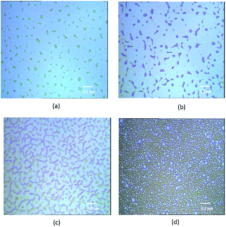 | ||
| Fig. 1 OM images of the AZO coated with (a) 0.1 wt%, (b) 0.3 wt%, (c) 0.6 wt% and (d) 0.9 wt% PVP. | ||
A solution consisting of P3HT (12 mg ml−1) and PCBM (10 mg ml−1) blend in chlorobenzene (CB) was spin-coated on either bare AZO or AZO/PVP layer and annealed at 120 °C for 10 min in air to form an P3HT:PCBM layer of about 200 nm thickness. PTB7![[thin space (1/6-em)]](https://www.rsc.org/images/entities/char_2009.gif) :PC71BM mixture with a ratio of 1:1.5 (PTB7 concentration of 10 mg ml−1) was dissolved in CB with 3% 1,8-diiodoctane (DIO). The photoactive layer of PTB7:PC71BM with a thickness of approximately 120 nm was prepared by spin-coating at 1000 rpm for 1 min. 5 nm MoO3 (HTL) and 100 nm Ag anodes were thermally evaporated through a shadow mask. The device active area was about 8 mm2. Reference devices without PVP layers were fabricated under the same conditions.
:PC71BM mixture with a ratio of 1:1.5 (PTB7 concentration of 10 mg ml−1) was dissolved in CB with 3% 1,8-diiodoctane (DIO). The photoactive layer of PTB7:PC71BM with a thickness of approximately 120 nm was prepared by spin-coating at 1000 rpm for 1 min. 5 nm MoO3 (HTL) and 100 nm Ag anodes were thermally evaporated through a shadow mask. The device active area was about 8 mm2. Reference devices without PVP layers were fabricated under the same conditions.
The surface morphology of PVP thin film was first observed by OM (Nikon ECLIPSE Ti-u) and the surface root-mean-square roughness (RMS) was characterized using atomic force microscopy (AFM) (Seiko SPA-400 SPM UNIT). J–V characteristics of the devices were measured under the illumination of an AM 1.5G (100 mW cm−2) solar simulator. The WF of the films was carried out using a Kelvin probe (KP020). The PL spectra of the samples were recorded using a steady-state fluorescence spectrometer (FL3-2-IHR221-NIR-TCSPC). Water contact angles were measured using a KRUSS (DSA100). Thick films were made under each weight ratio of PVP (0.1%, 0.3%, 0.6%, and 0.9%) by spin-coating five times. Then, these samples were measured using a Micro-figure measuring instrument (KOSAKA ET200). We improved the measurement precision by averaging the testing values of repeated ten measurements. The transmittance spectra of the samples were obtained using a Cary spectrophotometer (Cary 5000 UV-VIS).
The J–V characteristics and the dark J–V curves of P3HT:PCBM devices with different PVP interlayers are shown in Fig. 2(a) and (b). Detailed device performances are summarized in Table 1. By increasing the PVP weight ratio from 0% to 0.6%, the device performance was enhanced: the short current density (Jsc) increased from 8.05 to 11.32 mA cm−2, open circuit voltage (Voc) enhanced from 0.58 to 0.64 V, fill factor (FF) increased from 53.5% to 63.5% and PCE improved significantly from 2.50% to 4.55%. From Table 1, one can see that the photovoltaic parameters of IOSCs critically depend on the thickness of PVP interlayer: the device performance improved with increasing PVP thickness from 0 to 13 nm, while as the PVP thickness was increased continuously from 13 to 17 nm, all the parameters showed a slightly declining trend. It is clear that the improvement in the PCE of device mainly arose from the increased FF and Voc, and the devices with PVP interlayer having a thickness less than or more than 13 nm (0.6 wt%) show a decreased Jsc. This is because an interlayer that is very thin could not provide an ohmic contact for efficient electron extraction, while a very thick layer will lead to an increase in the series resistance (Rs).11 An ideal solar cell should have a low Rs and high shunt resistance (Rsh) to exhibit an optimized device performance.30 As listed in Table 1, the device Rs decreased from 16.44 to 6.06 Ω cm2, while the Rsh increased from 219.13 to 293.51 Ω cm2, indicating that contact quality between the AZO ETL and the active layer is significantly improved.19
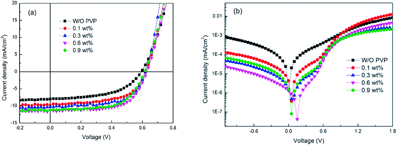 | ||
| Fig. 2 (a) J–V characteristics of the P3HT:PCBM cells with different weight ratios of PVP interlayer under AM 1.5G (100 mW cm−2) illumination. (b) J–V characteristics of the devices in the dark. | ||
| PVP [wt%] | RMS [nm] | Thickness [nm] | Contact angle [°] | Jsc [mA cm−2] | Voc [V] | FF [%] | PCE [%] | Rs [Ω cm2] | Rsh [Ω cm2] |
|---|---|---|---|---|---|---|---|---|---|
| 0 | 2.14 | — | 68.7 | 8.05 | 0.584 | 53.5 | 2.50 | 16.44 | 219.13 |
| 0.1 | 2.20 | ∼7 | 21.9 | 9.83 | 0.621 | 57.3 | 3.49 | 9.33 | 201.71 |
| 0.3 | 2.36 | ∼10 | 17.2 | 10.31 | 0.634 | 60.5 | 3.97 | 7.75 | 202.94 |
| 0.6 | 2.47 | ∼13 | 14.8 | 11.32 | 0.638 | 63.5 | 4.55 | 6.06 | 293.51 |
| 0.9 | 3.77 | ∼17 | 9.7 | 11.19 | 0.629 | 60.4 | 4.26 | 7.67 | 149.75 |
The lower leakage currents of PVP devices, as shown in Fig. 2(b), suggest that the built-in potential (Vbi) increases,38 which may strongly influence charge transport and extraction, increasing the device Voc.39 The Voc of the BHJ solar cell is mainly related to the difference between the highest occupied molecular orbital (HOMO) level of the donor (P3HT) and the lowest unoccupied molecular orbital (LUMO) level of the acceptor (PCBM).40 Meng et al. confirmed that there is a larger energy difference (ED) in HOMOd–LUMOa between PVP and PCBM than that between P3HT and PCBM.38 Moreover, the ED between P3HT/PVP is larger than that between P3HT/PCBM because the LUMO of PVP is higher than that of PCBM. Therefore, incorporating PVP creates a new transport pathway for the charges.41
In addition, the increased Vbi implies a lowered injection barrier in the inverted device. The PVP interlayer enhances the electron extraction near the cathode via lowering the work function (WF) of AZO and reduces the contact barrier between AZO ETL and the LUMO of the PCBM (acceptor) in the active layer. The energy alignment of the materials used in the IOSCs is shown in Fig. 3(a). After PVP layer deposition, the WF of the bare-AZO covered with 0.1, 0.3, 0.6, and 0.9 wt% PVP decreases from 4.89 eV to 4.76, 4.50, 4.42, and 4.30 eV, respectively, according to the results of the Kelvin probe (KP020) measurements. This indicates that the WF of AZO can be lowered effectively for the existence of pyrrolidone groups, and the reduction changed with the weight ratio of PVP. The energy band diagrams for the AZO/active layer junctions with and without a PVP layer are illustrated in Fig. 4(b), which takes the 0.6 wt% PVP interlayer as instance variables. The lowered WF of AZO ETL reduces the injection barrier, which primarily implies a decreased series resistance and is in good agreement with the discussion above (see Table 1).
 | ||
| Fig. 3 (a) Energy level [eV] diagram for each component material used in the P3HT:PCBM device. (b) The energy band diagrams for the AZO/active layer junctions with and without a PVP layer. | ||
 | ||
| Fig. 4 A schematic diagram of the mutual effect between the PVP polymer and the hydroxide radical on the ZnO surface. | ||
Furthermore, the dark J–V curve, presented in Fig. 2(b), demonstrates that the 0.1 wt% PVP device showed an improved rectification than that of the device without the PVP interlayer. The 0.3 wt% PVP devices showed an enhanced rectification followed by the 0.1 wt% devices. The 0.6 wt% PVP device shows a lower leakage and higher forward bias current. Its dark current densities are almost 100 times lower than that of the device without the PVP interlayer, which demonstrates that the PVP interlayer serves as an effective hole blocking layer, indicating that the recombination was suppressed the most after introducing a 0.6 wt% PVP interlayer.
We sought to further investigate the reason for the suppressed recombination. As mentioned above, PVP presents a non-conformal coverage on the AZO surface (see Fig. 1). Therefore, the PVP/AZO complex film can be deemed to form an organic (the PVP covered region)-inorganic (the AZO bared region) hybrid network. The defects with hydroxyl groups on the surface of the ZnO (AZO) thin film were formed during the sol–gel process at a low temperature.41–43 These hydroxyl groups are known to act as electron charge defect traps, which can affect not only the electrical properties at the interface between the metal oxide (AZO) and organic layers,44 but may also act as charge trap sites or recombination centers.45
On the one hand, leakage paths including pinholes in the films would be formed due to the existence of the defects. On the other hand, the recombination probability of charge carriers would increase while using the bare-ZnO (or bare-AZO) ETL when the carriers transit through the bulk heterojunction organic solar cells. This would lead to a great decrease in device performance.46 Moreover, the occurrence of an s-shape in the J–V characteristics is derived from recombination or low transport properties.25,47,48
Surface passivation using a functional layer has been reported, especially in interfacial dipole layers such as SAMs,25,30,46 conjugated polyelectrolytes15 and polyelectrolyte layers,49 which enhances the device performance by reducing the number of defects or trap-assisted recombination. In a previous work,33 a small interface dipole with a negative charge transferred from the PVP interlayer to the AZO ETL was found. However, the operating mechanism was not clear. H. Kozuka et al. found that the C![[double bond, length as m-dash]](https://www.rsc.org/images/entities/char_e001.gif) O groups of PVP were strongly bonded with the hydroxyl groups of the metalloxane polymers via hydrogen bonding.50 As a consequence, after the deposition of the PVP thin layer on the sol–gel AZO, the OH defects on the surface of AZO ETL can be compactly bonded with the CO groups of PVP by chemical adsorption (see the schematic diagram shown in Fig. 4). Correspondingly, the amount of OH group defects and the activity on the AZO surface is greatly eliminated after introducing a PVP interlayer. This was similar with the function of PVP during the sol–gel process.50–53 Such CO groups can be regarded as the “capping agent” for hydroxyl groups,51 obstructing their recombination with a hole, which would contribute to the enhancement of exciton dissociation efficiency.
O groups of PVP were strongly bonded with the hydroxyl groups of the metalloxane polymers via hydrogen bonding.50 As a consequence, after the deposition of the PVP thin layer on the sol–gel AZO, the OH defects on the surface of AZO ETL can be compactly bonded with the CO groups of PVP by chemical adsorption (see the schematic diagram shown in Fig. 4). Correspondingly, the amount of OH group defects and the activity on the AZO surface is greatly eliminated after introducing a PVP interlayer. This was similar with the function of PVP during the sol–gel process.50–53 Such CO groups can be regarded as the “capping agent” for hydroxyl groups,51 obstructing their recombination with a hole, which would contribute to the enhancement of exciton dissociation efficiency.
To further verify the exciton dissociation in the BHJ films, P3HT film and BHJ layers with PVP were investigated using photoluminescence (PL) measurements. As shown in Fig. 5(a), the broadband emission is greatly quenched, which is direct evidence for the reduced charge carrier recombination after the incorporation of the PVP thin films. In addition, a band to band emission of the AZO film at 396 nm is observed (see Fig. 5(b)) and the emission intensity increased slightly with the weight ratios of PVP. The change in the PL results supports our idea that the PVP interlayers do not disturb the crystallinity of the AZO film, whereas effectively decrease the carrier recombination at the interface of PVP/active layer, which improves the exciton dissociation, and thus higher performance is expected.
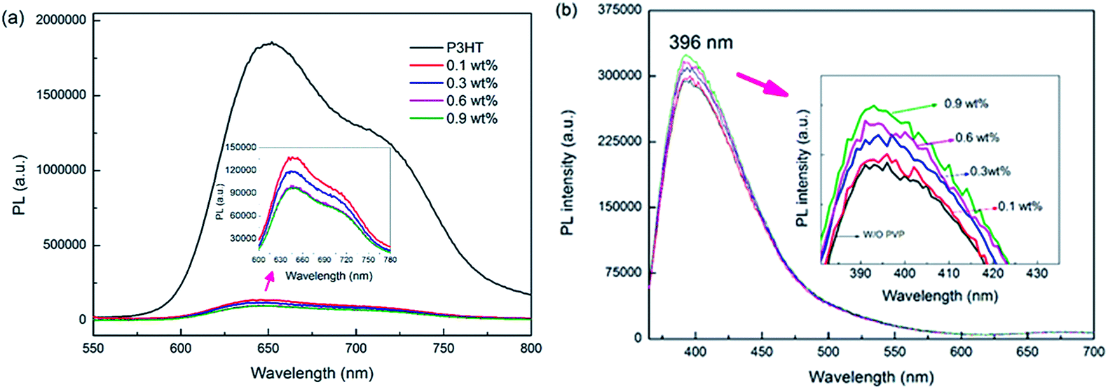 | ||
| Fig. 5 (a) PL spectra of the P3HT and BHJ films with different weight ratios of PVP. (b) PL spectra of the AZO film coated with different weight ratios of PVP. | ||
The reduction in surface defect traps lead to a better contact.30 As shown in Fig. 4,33 the wettability of the AZO/ITO substrate increases and the water contact angle decreases obviously after the introduction of PVP interlayer. To further determine the change in wettability as a function of PVP thickness, the surface energy of AZO with different PVP layers was studied with water contact angle measurements. As displayed in Table 1, the water contact angle decreases from 68.7° for the bare-AZO film to 9.7° for the 0.9 wt% PVP, indicating that the hydrophilicity of these films is increased evidently with increasing thickness of PVP. The better hydrophilic properties allow an intimate contact, leading to a better surface quality; this can provide better wettability and adhesion with the active layer.54
The modified surface morphology improves the device performance.55 The morphologies of PVP/AZO layers were examined using AFM and the results are shown in Fig. 6. The PVP layer formed an incomplete coverage on the AZO ETL with a gradually increased RMS from 2.20 to 3.77 nm (see Table 1) when the PVP weight ratio was increased from 0.1 to 0.9 wt%. The rougher surface of the PVP layer means a strong interfacial adhesion7 between the ETL and P3HT:PCBM layer.
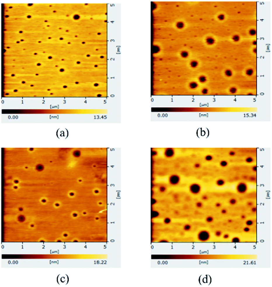 | ||
| Fig. 6 AFM images of the AZO coated with 0.1 (a), 0.3 (b), 0.6 (c) and 0.9 wt% (d) PVP. | ||
Furthermore, we studied the dependence of the optical transmittance properties of the PVP/AZO composite films on the PVP film thickness. The transmittance spectra, shown in Fig. 7, suggest that there is a small increase in the transmittance of the PVP coated samples with increasing PVP weight ratio, which contributes to the increase in the Jsc of the device.55 However, increase in the transparency of 0.9 wt% PVP does not contribute to the device performance. We believe the reason may still be connected with its thickness.
 | ||
| Fig. 7 Transmittance spectra of AZO with and without PVP layers at wavelengths ranging from 300 to 750 nm. | ||
Based on the above discussion, the PVP interlayer with the proper thickness (∼13 nm) can be more effective to provide an ohmic contact between AZO ETL and the active layer for electron extraction. Upon successful attempts on the P3HT:PCBM device, we explored the applicability of the PVP interfacial layer to low bandgap polymer solar cells. The same procedure on IOSCs based on the PTB7:PC71BM copolymer was conducted. Detailed device performance is listed in Table 2. The J–V characteristic curves for PTB7:PC71BM cells under illumination and in the dark are presented in Fig. 8. In contrast to the cell without the PVP interlayer, the PTB7:PC71BM device exhibited a significant increase in FF (54.3% versus 49.7%) and Voc (0.701 V versus 0.638 V). Together with the reduced Rs (8.93 versus 8.02 Ω cm2) and greatly improved Rsh (408.64 versus 2163.83 Ω cm2) (see Table 2), it can be suggested that the interface contact quality between the AZO ETL and the active layer was improved remarkably after inserting the PVP layer. Moreover, charge carrier transfer becomes more effective due to the suppressed recombination.
| PVP [wt%] | Jsc [mA cm−2] | Voc [V] | FF [%] | PCE [%] | Rs [Ω cm2] | Rsh [Ω cm2] |
|---|---|---|---|---|---|---|
| 0 | 13.92 | 0.638 | 49.7 | 4.42 | 8.94 | 408.64 |
| 0.6 | 16.23 | 0.701 | 54.3 | 6.18 | 8.02 | 2163.83 |
 | ||
| Fig. 8 (a) J–V characteristics of the PTB7:PC71BM cells with and without the PVP layer under AM 1.5G (100 mW cm−2) illumination. (b) J–V characteristics of the devices in the dark. | ||
In summary, inverted organic solar cells with a solution-processed PVP interface modifier with varying thickness were investigated. The thickness of the PVP layers played a direct and important role in the contact quality between the AZO ETL and the active layer. An ∼13 nm PVP interlayer could obtain a significant improvement in the performance of the P3HT:PCBM and PTB7:PC71BM devices, due to the decrease in the contact barrier and reduced hydroxide radical amount as well as the effect of the charge transfer at the interface to reduce the charge recombination.
This study opens up an alternative method to improve the ZnO (AZO) surface properties for the interface design of IOSCs. In addition, we believe that the PVP interfacial modification is not limited to the two polymers utilized here. Together with marked advantages than other interfacial materials during their preparation, our results provide a valuable reference for improving the performance of inverted organic solar cells to meet the industrial fabrication level.
Acknowledgements
The authors gratefully acknowledge the National Natural Science Foundation of China (Grant No. 61377031) and Scientific Research Foundation (Q1444) of Zhejiang Ocean University.References
- M. Hösel, H. F. Dam and F. C. Krebs, Energy Technol., 2015, 3, 293–304 CrossRef PubMed.
- F. C. Krebs, Sol. Energy Mater. Sol. Cells, 2009, 93, 465–475 CrossRef CAS PubMed.
- F. C. Krebs, N. Espinosa, M. Hösel, R. R. Søndergaard and M. Jørgensen, 25th Anniversary Article: Rise to Power-OPV-Based Solar Parks, Adv. Mater., 2014, 26, 29–39 CrossRef CAS PubMed.
- C. J. Brabec, S. Gowrisanker, J. J. M. Halls, D. Laird, S. Jia and S. P. Williams, Adv. Mater., 2010, 22, 3839–3856 CrossRef CAS PubMed.
- J. Adams, G. D. Spyropoulos, M. Salvador, N. Li, S. Strohm, L. Lucera, S. Langner, F. Machui, H. Zhang, T. Ameri, M. M. Voigt, F. C. Krebsc and C. J. Brabec, Energy Environ. Sci., 2015, 8, 169–176 CAS.
- F. Padinger, R. S. Rittberger and N. S. Sariciftci, Adv. Funct. Mater., 2003, 13, 85–88 CrossRef CAS PubMed.
- W. Ma, C. Y. X. Gong, K. Lee and A. J. Heeger, Adv. Funct. Mater., 2005, 15, 1617–1622 CrossRef CAS PubMed.
- J. H. Park, J. S. Kim, J. H. Lee, W. H. Lee and K. Cho, J. Phys. Chem. C, 2009, 113, 17579–17584 CAS.
- J. S. Moon, J. Jo and A. J. Heeger, Adv. Energy Mater., 2012, 2, 304–308 CrossRef CAS PubMed.
- X. Li, W. C. H. Choy, L. Huo, F. Xie, W. E. I. Sha, B. Ding, X. Guo, Y. Li and J. Hou, Adv. Mater., 2012, 24, 3046–3052 CrossRef CAS PubMed.
- Z. He, C. Zhong, S. Su, M. Xu, H. Wu and Y. Cao, Nat. Photonics, 2012, 6, 593–597 CrossRef CAS PubMed.
- Q. Zhang, B. Kan, F. Liu, G. Long, X. Wan, X. Chen, Y. Zuo, W. Ni, H. Zhang, M. Li, Z. Hu, F. Huang, Y. Cao, Z. Liang, M. Zhang, T. P. Russell and Y. Chen, Nat. Photonics, 2015, 9, 35–41 CrossRef CAS PubMed.
- H. Cao, W. He, Y. Mao, X. Lin, K. Ishikawa, J. H. Dickerson and W. P. Hess, J. Power Sources, 2014, 264, 168–183 CrossRef CAS PubMed.
- M. Jorgensen, K. Norrman and F. C. Krebs, Sol. Energy Mater. Sol. Cells, 2008, 92, 686–714 CrossRef PubMed.
- T. Yang, M. Wang, C. Duan, X. Hu, L. Huang, J. Peng, F. Huang and X. Gong, Energy Environ. Sci., 2012, 5, 8208–8214 CAS.
- S. K. Hau, H.-L. Yip, N. S. Baek, J. Zou, K. O'Malley and A. K.-Y. Jen, Appl. Phys. Lett., 2008, 92, 253301 CrossRef PubMed.
- S. Sanchez, S. Berson, S. Guillerez, C. L. Clement and V. Ivanova, Adv. Energy Mater., 2012, 2, 541–545 CrossRef CAS PubMed.
- J. Weickert, H. Sun, C. Palumbiny, H. C. Hesse and L. S. Mende, Sol. Energy Mater. Sol. Cells, 2010, 94, 2371–2374 CrossRef CAS PubMed.
- Z. Liang, Q. Zhang, O. Wiranwetchayan, J. Xi, Z. Yang, K. Park, C. Li and G. Cao, Adv. Funct. Mater., 2012, 22, 2194–2201 CrossRef CAS PubMed.
- K. S. Shin, K. H. Lee, H. H. Lee, D. Choi and S. W. Kim, J. Phys. Chem. C, 2010, 114, 15782–15785 CAS.
- H. Oh, J. Krantz, I. Litzov, T. Stubhan, L. Pinna and C. J. Brabec, Sol. Energy Mater. Sol. Cells, 2011, 95, 2194–2199 CrossRef CAS PubMed.
- A. Aprilia, P. Wulandari, V. Suendo, Herman, R. Hidayat, A. Fujii and M. Ozaki, Sol. Energy Mater. Sol. Cells, 2013, 111, 181–188 CrossRef CAS PubMed.
- T. Stubhan, H. Oh, L. Pinna, J. Krantz, I. Litzov and C. J. Brabec, Org. Electron., 2011, 12, 1539–1543 CrossRef CAS PubMed.
- R. Søndergaard, M. Helgesen, M. Jørgensen and F. C. Krebs, Adv. Energy Mater., 2011, 1, 68–71 CrossRef PubMed.
- T. Stubhan, M. Salinas, A. Ebel, F. C. Krebs, A. Hirsch, M. Halik and C. J. Brabec, Adv. Energy Mater., 2012, 2, 532–535 CrossRef CAS PubMed.
- C. H. Hsieh, Y. J. Cheng, P. J. Li, C. H. Chen, M. Dubosc, R. M. Liang and C. S. Hsu, J. Am. Chem. Soc., 2010, 132, 4887–4893 CrossRef CAS PubMed.
- H. Ma, H.-L. Yip, F. Huang and A. K. Y. Jen, Adv. Funct. Mater., 2010, 20, 1371–1388 CrossRef CAS PubMed.
- R. Po, C. Carbonera, A. Bernardi and N. Camaioni, Energy Environ. Sci., 2011, 4, 285–310 CAS.
- H.-L. Yip and A. K. Y. Jen, Energy Environ. Sci., 2012, 5, 5994–6011 CAS.
- S. K. Hau, H.-L. Yip, O. Acton, N. S. Baek, H. Ma and A. K. Y. Jen, J. Mater. Chem., 2008, 18, 5113–5119 RSC.
- Y.-J. Cheng, F.-Y. Cao, W.-C. Lin, C.-H. Chen and C.-H. Hsieh, Chem. Mater., 2011, 23, 1512–1518 CrossRef CAS.
- C. Gu, Y. Chen, Z. Zhang, S. Xue, S. Sun, C. Zhong, H. Zhang, Y. Lv, F. Li, F. Huang and Y. Ma, Adv. Energy Mater., 2014, 4, 1301771 Search PubMed.
- X. Yu, X. Yu, J. Zhang, G. Zhao, J. Ni, H. Cai and Y. Zhao, Sol. Energy Mater. Sol. Cells, 2014, 128, 307–312 CrossRef CAS PubMed.
- S. K. Hau, Y. J. Cheng, H. L. Yip, Y. Zhang, H. Ma and A. K. Y. Jen, ACS Appl. Mater. Interfaces, 2010, 2, 1892–1902 CAS.
- J. W. Shim, H. Cheun, J. Meyer, C. F. Hernandez, A. Dindar, Y. H. Zhou, D. K. Hwang, A. Kahn and B. Kippelen, Appl. Phys. Lett., 2012, 101, 073303-1–073303-4 Search PubMed.
- L. Lu and L. Yu, Adv. Mater., 2014, 26, 4413–4430 CrossRef CAS PubMed.
- M. J. Alam, D. C. Cameron, M. Alam and D. Cameron, J. Vac. Sci. Technol., A, 2001, 19, 1642–1646 CAS.
- F. Meng, S. Liu, Y. Wang, C. Tao, P. Xu, W. Guo, L. Shen, X. Zhang and S. Ruan, J. Mater. Chem., 2012, 22, 22382–22386 RSC.
- Z. He, C. Zhong, X. Huang, W. Y. Wong, H. Wu, L. Chen, S. Su and Y. Cao, Adv. Mater., 2011, 23, 4636–4643 CrossRef CAS PubMed.
- G. Dennler, M. C. Scharber and C. J. Brabec, Adv. Mater., 2009, 21, 1323–1338 CrossRef CAS PubMed.
- S. H. Liao, H. J. Jhuo, Y. S. Cheng and S. A. Chen, Adv. Mater., 2013, 25, 4766–4771 CrossRef CAS PubMed.
- M. Chen, X. Wang, Y. H. Yu, Z. L. Pei, X. D. Bai, C. Sun, R. F. Huang and L. S. Wen, Appl. Surf. Sci., 2000, 158, 134–140 CrossRef CAS.
- J. Wang, Z. Wang, B. Huang, Y. Ma, Y. Liu, X. Qin, X. Zhang and Y. Dai, ACS Appl. Mater. Interfaces, 2012, 4, 4024–4030 CAS.
- L. L. Chua, J. Zaumseil, J. F. Chang, E. C. W. Ou, P. K. H. Ho, H. Sirringhaus and R. H. Friend, Nature, 2005, 434, 194–199 CrossRef CAS PubMed.
- X. Chen, L. Liu, P. Y. Yu and S. S. Mao, Science, 2011, 33, 746–750 CrossRef PubMed.
- H. Yip, S. K. Hau, N. S. Baek, H. Ma and A. K.-Y. Jen, Adv. Mater., 2008, 20, 2376–2382 CrossRef CAS PubMed.
- A. Wagenpfahl, D. Rauh, M. Binder, C. Deibel and V. Dyakonov, Phys. Rev. B: Condens. Matter Mater. Phys., 2010, 82, 115306 CrossRef.
- R. Steim, F. R. Koglera and C. J. Brabec, J. Mater. Chem., 2010, 20, 2499–2512 RSC.
- A. K. K. Kyaw, D. H. Wang, V. Gupta, J. Zhang, S. Chand, G. C. Bazan and A. J. Heeger, Adv. Mater., 2013, 25, 2397–2402 CrossRef CAS PubMed.
- H. Kozuka, S. Takenaka, H. Tokita and M. Okubayashi, J. Eur. Ceram. Soc., 2004, 24, 1585–1588 CrossRef CAS.
- S. Linardos, Q. Zhang and J. R. Alcock, J. Eur. Ceram. Soc., 2006, 26, 117–123 CrossRef CAS PubMed.
- Y. Kimura, D. Abe, T. Ohmori, M. Mizutani, M. Harada, Y. Kimura, D. Abe, T. Ohmori, M. Mizutani and M. Harada, Colloids Surf., A, 2003, 231, 131–141 CrossRef CAS PubMed.
- L. Liang, L. Zhang, Y. Sheng, Y. Xu, D. Wu, Y. Sun, X. Jiang and X. Wei, Acta Phys. Sin., 2007, 56, 3596–3601 CAS.
- R. Steim, S. A. Choulis, P. Schilinsky and C. J. Brabec, Appl. Phys. Lett., 2008, 92, 093303 CrossRef PubMed.
- C. E. Small, S. Chen, J. Subbiah, C. M. Amb, S. W. Tsang, T. H. Lai, J. R. Reynolds and F. So, Nat. Photonics, 2012, 6, 115–120 CrossRef CAS PubMed.
Footnote |
| † Xuan Yu and Xiaoming Yu contributed equally to this work. |
| This journal is © The Royal Society of Chemistry 2015 |