
Electric-field induced layer-by-layer assembly technique with single component for construction of conjugated polymer films†
Shiwei Wanga,
Zhuo Chena,
Ahmad Umarb,
Yao Wang*a and
Peng-gang Yina
aKey Laboratory of Bio-Inspired Smart Interfacial Science and Technology of Ministry of Education, School of Chemistry and Environment, Beihang University, Beijing 100191, P R China. E-mail: yao@buaa.edu.cn; wswjldx2004@163.com; Fax: +86-10-82317801; Tel: +86-10-82317801
bDepartment of Chemistry, Faculty of Science and Arts, Promising Centre for Sensors and Electronic Devices, Najran University, Najran 11001, P.O.Box-1988, Kingdom of Saudi Arabia
First published on 29th June 2015
Abstract
Conjugated polymer (CP) multilayer films with higher conductivity have been constructed by electric-field induced LBL assembly technique. Single component has been selected in the alternate deposition process, which not only provides a universal approach for CP films fabrication but also broadens the applicable scope of LBL assembly technique.
The layer-by-layer (LBL) assembly technique has always been considered to be one of the most versatile thin-film processing strategies for the construction of devices in nano-scale using varieties of polymers,1–4 inorganic nano-particles,5,6 and biological molecules.7–9 By utilizing the LBL technique, complex multilayer thin films of tailored thickness, composition, and structure could be prepared on planar or curved surfaces under the driving forces of electrostatic interactions,10–12 hydrogen bonding,13–19 coordination bonding, and so on.20,21 But anyway, at least two kinds of active molecules cyclically deposition was required during the operation of LBL technique in previous studies,22–26 which severely limited the development and application range of the advanced technology. It will be great progress if LBL assembly can be developed by any single component.
Conjugated polymers (CPs) have attracted much attention because of their potential optoelectronic applications such as polymer light-emitting diodes (PLEDs), photovoltaic devices and field-effect transistors.27–31 Traditionally, high-quality semiconductor films with high molecule crystallization can be formed by spin-coating or ink-jet printing technique following the post-processing, which has been widely used in the preparation of optoelectronic devices.32–34 However, these methods were not adapt to fabricate CPs film in large area,35,36 and they are environment contaminative, wasteful and complex.37–40
In this communication, CPs multilayer thin films have been successfully constructed by cyclically depositions of single component of CP molecules under electric-field (EF), which not only provided a new approach to construct CPs films with high quality in large area, but also greatly broadened the application range of LBL assembly technique. By EF induced LBL assembly technique,41 the thickness of CP thin films can be precisely controlled in molecular level and the high crystallization of CP molecules in corresponding thin films can be achieved easily, meanwhile, the operation of which was simple and efficient without any pollution, because the solvent can be recycled and reused.
Herein, as a proof-of-concept for this method, the well-known and typical CP of poly(3-hexylthiophene) (P3HT, Mw = 15![[thin space (1/6-em)]](https://www.rsc.org/images/entities/char_2009.gif) 000) was selected as a model structure in this work. Scheme 1 shows and outlines the installation and approaches to the construction of P3HT LBL multilayer film. The ITO glasses were dipped in H2O2 for 12 hours, rinsed thoroughly with Millipore water, further rinsed with pure ethanol, and then dried under a 0.55 μm filtered stream of dry N2. Immersion of the cleaned ITO glass substrate in P3HT solution (0.01 M) under the 10 V DC voltage (the distances between the substrate and the counter electrode was 2 mm) for 10 min, then dried with N2. Repetition of this procedure enables the fabrication of thin films with a large number of layers (ESI†).
000) was selected as a model structure in this work. Scheme 1 shows and outlines the installation and approaches to the construction of P3HT LBL multilayer film. The ITO glasses were dipped in H2O2 for 12 hours, rinsed thoroughly with Millipore water, further rinsed with pure ethanol, and then dried under a 0.55 μm filtered stream of dry N2. Immersion of the cleaned ITO glass substrate in P3HT solution (0.01 M) under the 10 V DC voltage (the distances between the substrate and the counter electrode was 2 mm) for 10 min, then dried with N2. Repetition of this procedure enables the fabrication of thin films with a large number of layers (ESI†).
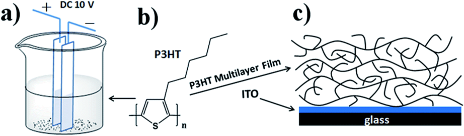 | ||
| Scheme 1 (a) The installation and process of the construction of P3HT multilayer film by electric-field-induced layer-by-layer assembly technique; (b) the molecular structure of P3HT; (c) the schematic diagram of P3HT multilayer film. | ||
The build-up of the multilayer was monitored by UV-vis spectroscopy. Fig. 1a shows the UV-vis absorption spectra of a P3HT multilayer film with different number of layers on an ITO substrate surface. The color of the sample would become deeper and deeper with the increasing of deposition layer, but all the data was obtained by the same substrate and P3HT solution, so we can confirm that the variation of UV absorption intensity was originated from P3HT molecules. The absorption maximum at 608 nm and 523 nm was attributed to the absorption of the π–π* transition of the polymer backbone. The linear increase of the absorbance at 608 nm and 523 nm with the increase of the number of deposited layers confirmed that an equal amount of P3HT was deposited in each deposition cycle (Fig. 1b), which also indicated that it was a stepwise and uniform assembly process.
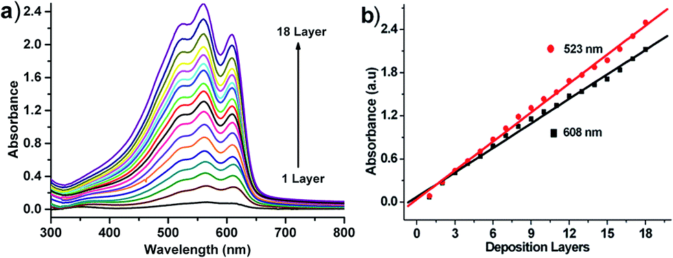 | ||
| Fig. 1 (a) UV-vis absorption spectra of 18 layers P3HT films with different number of deposition cycles; (b) the variation between the absorption at 523 and 608 nm and the number of mono-layer assembled under a 10 V DC voltage EF. | ||
UV-vis spectroscopy was also employed to study the deposition kinetics of CPs under the EF induced effect. As shown in Fig. 2, there was a significant enhancement of UV-vis characteristic absorption peak for P3HT bilayer film without EF at 100 °C as compared with the one at room temperature, and it was the strongest for the film deposited on the negative pole at 100 °C, which was in contrast to the positive electrode. It was a normal regulation for the polymer film formation with the volatilization of solution under high temperature, but the larger amounts of P3HT molecules deposited on the substrate was attributed to the effect of EF. It can be generalized from the results that the deposition of P3HT film and the dissolution of P3HT solute is a balanced state, and the effect of the EF can promote the formation of P3HT thin film, which is oriented orderly deposition. P3HT molecule will be desorbed from the anode and directionally deposited on the cathode substrate under EF. In other words, the driving force of P3HT multilayer film is attributed to the solution volatilization and EF, meanwhile, EF can control the deposition direction and intensity of CPs. In this work, 10 min was selected as the deposition time for each layer of CP film under EF, because after 10 min, the intensity of UV absorbance peak was never increased with the deposition time. After deposition of one layer of CPs, solvent left in the films would be dried by pure N2, then the orientation of CP molecules in film would be fixed and high quality CP multilayer layer film in a certain thickness would be formed. The thickness of 10 layers P3HT film was nearly 200 nm, corresponding to an average thickness of 20 nm for one layer of assembled film, which was measured by step profiler. The thickness variation of P3HT multilayer film with deposition layers was shown in Fig. S1 of ESI.†
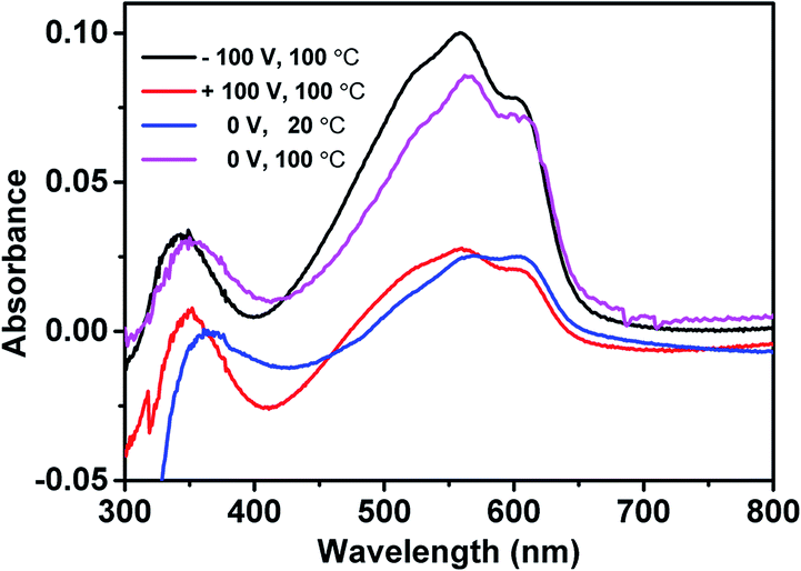 | ||
| Fig. 2 UV-vis absorption spectra of 2 layers P3HT films under different electrode, temperature and voltage during the fabrication process. | ||
It is worth mentioning that 10 V DC voltage was found to be the most appropriate for the system from the verification of numerous comparative tests. The extent of the film deposition was quite weak when the voltage was lower than 10 V, which was rather insignificant and inefficient. However, if the voltage was more than 10 V, it was difficult to form high quality multilayer film and power shortage could occur easily between the electrodes, resulting in the destruction of the film (Fig. S2, ESI†).
As previous literature42,43 reported, P3HT thin films with certain thickness can be formed by electric deposition technique, but the thickness will not be increased in certain time because of the molecules balance in solution. In ordinary conditions, π-electron in CP molecule can move freely and distribute evenly in the conjugated chain in statistics. That is symmetrical electron cloud distribution in the molecular structure of CP. When EF is added in CP solution, π-electron in CP molecule will be moved directionally and the electron cloud will be distributed asymmetrically due to electrostatic interactions, and dipoles have been developed in CPs. Conversely, CPs with dipolar structure near the electrode will be deposited onto the electrode directionally and consistently under the effect of DC EF.44 In this work, after a layer of CP was deposited under EF from the solution, the solvent was blow-dried fast and the polymer chain would be entwined firmly. Repeated the cycles, oriented and ordered multilayer CP films with high quality would be formed. The mechanism and the effect process are sketched as in Fig. 3, which are universal for CP molecules. We believe that the technique and concept is significance and beneficial to scientists not only in theoretical research but also in practical application in related fields.
 | ||
| Fig. 3 The mechanism and the variation process of the electronic cloud of conjugated polymer in its solution under DC electric-field, and the digital photo of the multilayer P3HT films on ITO glass. | ||
Further, in order to verify the universality of the EF induced LBL assembly technique for construction of CP multilayer films, another representative CP of poly(9,9-dioctylfluorene) (PFO) (see Fig. S4, ESI†) was selected to repeat the above process of EF induced assembly. The operation steps for PFO were the same as ones for P3HT mentioned before. The variation trend (Fig. S5†) and the linear relationship (Fig. S6†) of the corresponding UV-vis absorption spectra of PFO assembly process were all highly coincident with the ones of P3HT assembled films, which evidently illustrates that EF induced LBL assembly method is universal on construction of mono-component CPs multilayer films.
The surface morphology of the P3HT multilayer films was examined using tapping mode atomic force microscopy (AFM). The AFM height image of the 5-layer film shown in Fig. 4 reveals remarkably homogeneous coverage of the LBL film. The root mean square (rms) roughness was calculated to be about 1.934 nm (for 10 μm × 10 μm areas), where the ITO glass substrate and the spin-coating P3HT film has an initial rms roughness of ∼1.969 nm and 1.838 nm, respectively. The surface roughness is comparable to conventional polyelectrolyte LBL films (i.e. typically in the range of 10–30 Å), which further indicates that the obtained P3HT multilayer films here are of high quality.
 | ||
| Fig. 4 (a) The high diagram of atomic force microscope (AFM) images on tapping mode at 10 × 10 μm2 areas of (a) ITO glass, (b) P3HT spin-coating film and (c) 5 layers P3HT assembled films. | ||
High crystallization of CP molecules in films was necessary for fabricating devices as an active layer, such as organic photovoltaic cells, bioassays and thin film transistor. The crystallization of P3HT multilayer film fabricated by EF induced LBL assembly was greatly improved as compared with the spin-coating film in the same thickness without any post-processing (Fig. 5), which was the inevitable result that directional and orderly deposition of CP in molecular level. High crystallization and ordered arrangement of P3HT molecules in the film was certainly beneficial to the translation of electronics, I–V curves test has been used to confirm the mechanism (Fig. 6). It can be calculated that the planar resistance of the assembled P3HT film (9.46 × 10⁶ Ω) was obviously lower than the spin-coating one (4.46 × 10⁷ Ω), so the multilayer CP film with high conductance has been successfully obtained by electric-field induced assembly technique. The detailed characterization, mechanism research and device fabrication are ongoing in our lab.
 | ||
| Fig. 5 The XRD profiles of P3HT films with the same thickness fabricated by spin-coating and EF induced LBL assembly (18 layers). | ||
 | ||
| Fig. 6 The current–voltage (I–V) curves on the surface of P3HT films fabricated by spin-coating and LBL assembly technique (15 layers), here, platina was used as the electrode by laser ablation and the distance between electrodes was about 800 μm. | ||
Conclusions
In summary, EF induced LBL assembly technique has been successfully developed for the assembly of multilayer CPs thin films with controlled thickness, high quality and high conductance. Single polymer component was selected during the multilayer thin films fabricating process, which broadened the range of the LBL technique and provided a solution to the problem of preparing ordered CP with high crystallinity in thin films directly without any after-treatment process. This approach can be readily applied to a wide range of conducting polymers, thereby offering more possibilities to the implementation of novel supramolecular assembly films with extraordinary cooperative electronic and photonic properties.Acknowledgements
The authors gratefully acknowledge funding of this research by the National Natural Science Foundation of China (Grant No. 21204087, 51373005), Project Funded by China Postdoctoral Science Foundation (2015M570022), Program for New Century Excellent Talents in University (NCET-10-0035), National Key Basic Research Program of China (2014CB931800) and Fundamental Research Funds for the Central Universities. We are further grateful to Changchun Institute of Applied Chemistry, Chinese Academy of Sciences, which is the project support unit of NSFC-No. 21204087.Notes and references
- Y. N. Li, H. Huang, Y. Li and X. G. Su, Sens. Actuators, B, 2013, 188, 772 CrossRef CAS PubMed.
- J. W. Jeon, J. O'Neal, L. Shao and J. L. Lutkenhaus, ACS Appl. Mater. Interfaces, 2013, 5, 10127 CAS.
- C. A. Nguyen, A. A. Argun, P. T. Hammond, X. H. Lu and P. S. Li, Chem. Mater., 2011, 23, 2142 CrossRef CAS.
- K. Y. K. Man, H. L. Wong, W. K. Chan, A. B. Djurisic, E. Beach and S. Rozeveld, Langmuir, 2006, 22, 3368 CrossRef CAS PubMed.
- T. Cassagneau, T. E. Mallouk and J. H. Fendler, J. Am. Chem. Soc., 1998, 120, 7848 CrossRef CAS.
- J. Kim, S. W. Lee, P. T. Hammond and Y. S. Horn, Chem. Mater., 2009, 21, 2993 CrossRef CAS.
- H. Ai, M. Fang, S. A. Jones and Y. M. Lvov, Biomacromolecules, 2002, 3, 560 CrossRef CAS PubMed.
- R. Wilson, M. Mehrabi, I. A. Prior, A. Beckett and A. Hutchinson, Chem. Commun., 2009, 18, 2487 RSC.
- D. L. Elbert, C. B. Herbert and J. A. Hubbell, Langmuir, 1999, 15, 5355 CrossRef CAS.
- T. J. Tang, J. Q. Qu, K. Mulllen and S. E. Webber, Langmuir, 2006, 22, 26 CrossRef CAS PubMed.
- F. Auer, M. Scotti, A. Ulman, R. Jordan, B. Sellergren, J. Garno and G. Y. Liu, Langmuir, 2000, 16, 7554 CrossRef CAS.
- L. Cheng and S. J. Dong, Electrochem. Commun., 1999, 1, 159 CrossRef CAS.
- S. A. Sukhishvili and S. Granick, Macromolecules, 2002, 35, 301 CrossRef CAS.
- A. Zhuk, S. Pavlukhina and S. A. Sukhishvili, Langmuir, 2009, 25, 14025 CrossRef CAS PubMed.
- Y. Zhao, J. Bertrand, X. Tong and Y. Zhao, Langmuir, 2009, 25, 13151 CrossRef CAS PubMed.
- E. Kharlampieva, V. Kozlovskaya and S. A. Sukhishvili, Adv. Mater., 2009, 21, 3053 CrossRef CAS PubMed.
- G. H. Zeng, J. Gao, S. L. Chen, H. Chen, Z. Q. Wang and X. Zhang, Langmuir, 2007, 23, 11631 CrossRef CAS PubMed.
- E. Kharlampieva and S. A. Sukhishvili, J. Macromol. Sci., Part C: Polym. Rev., 2006, 46, 377 CrossRef CAS PubMed.
- Z. Q. Liang, O. M. Cabarcos, D. L. Allara and Q. Wang, Adv. Mater., 2004, 16, 823 CrossRef CAS PubMed.
- W. Zhao, B. Tong, J. B. Shi, Y. X. Pan, J. B. Shen, J. G. Zhi, W. K. Chan and Y. P. Dong, Langmuir, 2010, 26, 16084 CrossRef CAS PubMed.
- V. Stepanenko, M. Stocker, P. Muller, M. Buchner and F. Wurthner, J. Mater. Chem., 2009, 19, 6816 RSC.
- L. Li, R. Z. Ma, Y. Ebina, K. Fukuda, K. Takada and T. Sasaki, J. Am. Chem. Soc., 2007, 129, 8000 CrossRef CAS PubMed.
- B. Qi, X. Tong and Y. Zhao, Macromolecules, 2006, 39, 5714 CrossRef CAS.
- O. Crespo-Biel, B. Dordi, D. N. Reinhoudt and J. Huskens, J. Am. Chem. Soc., 2005, 127, 7594 CrossRef CAS PubMed.
- L. X. Shi, Y. X. Lu, J. Sun, J. Zhang, C. Q. Sun, J. Q. Sun and J. C. Shen, Biomacromolecules, 2003, 4, 1161 CrossRef CAS PubMed.
- R. J. Pei, X. Q. Cui, X. R. Yang and E. K. Wang, Biomacromolecules, 2001, 2, 463 CrossRef CAS PubMed.
- C. H. Duan, K. Zhang, X. Guan, C. M. Zhong, H. M. Xie, F. Huang, J. W. Chen, J. B. Peng and Y. Cao, Chem. Sci., 2013, 4, 1298 RSC.
- A. Facchetti, Chem. Mater., 2011, 23, 733 CrossRef CAS.
- D. Sahu, H. Padhy, D. Patra, J. H. Huang, C. W. Chu and H. C. Lin, J. Polym. Sci., Part A: Polym. Chem., 2010, 48, 5812 CrossRef CAS PubMed.
- C. C. Chueh, M. H. Lai, J. H. Tsai, C. F. Wang and W. C. Chen, J. Polym. Sci., Part A: Polym. Chem., 2010, 48, 74 CrossRef CAS PubMed.
- M. H. Lai, C. C. Chueh, W. C. Chen, J. L. Wu and F. C. Chen, J. Polym. Sci., Part A: Polym. Chem., 2009, 47, 973 CrossRef CAS PubMed.
- T. Q. Nguyen and B. J. Schwartz, J. Chem. Phys., 2002, 116, 8198 CrossRef CAS PubMed.
- C. C. Chang, C. L. Pai, W. C. Chen and S. A. Jenekhe, Thin Solid Films, 2005, 479, 254 CrossRef CAS PubMed.
- D. Y. Khim, W. H. Lee, K. J. Baeg, D. Y. Kim, I. N. Kang and Y. Y. Noh, J. Mater. Chem., 2012, 22, 12774 RSC.
- C. M. Amb, M. R. Craig, U. Koldemir, J. Subbiah, K. R. Choudhury, S. A. Gevorgyan, M. Jørgensen, F. C. Krebs, F. So and J. R. Reynolds, ACS Appl. Mater. Interfaces, 2012, 4, 1847–1853 CAS.
- M. Noebels, R. E. Cross, D. A. Evans and C. E. Finlayson, J. Mater. Sci., 2014, 49, 4279 CrossRef CAS.
- Y. Li, S. S. Chen, M. C. Wu and J. Q. Sun, Adv. Mater., 2014, 26, 3344 CrossRef CAS PubMed.
- X. Wang, Y. Wang, S. Bi, Y. G. Wang, X. G. Chen, L. Y. Qiu and J. Q. Sun, Adv. Funct. Mater., 2014, 24, 403 CrossRef CAS PubMed.
- K. Y. K. Man, H. L. Wong, W. K. Chan, B. Djurisic, E. Beach and S. Rozeveld, Langmuir, 2006, 22, 3368 CrossRef CAS PubMed.
- M. C. Quiles, M. I. Alonso, D. D. C. Bradley and L. J. Richter, Adv. Funct. Mater., 2014, 24, 2116 CrossRef PubMed.
- Y. Wang, X. J. Wang, Y. Guo, Z. C. Cui, Q. Lin, W. Z. Yu, L. Xu, D. M. Zhang and B. Yang, Langmuir, 2004, 20, 8952 CrossRef CAS PubMed.
- S. Miyajima, S. Nagamatsu, S. S. Pandey, S. Hayase, K. Kaneto and W. Takashima, Appl. Phys. Lett., 2012, 101, 193305 CrossRef PubMed.
- M. Ammam, RSC Adv., 2012, 2, 7633 RSC.
- S. W. Wang, Z. Chen and Y. Wang, Chem. Commun., 2015, 51, 765 RSC.
Footnote |
| † Electronic supplementary information (ESI) available: Detailed experimental procedures, voltage selection, transparency and the relationship between assemble layers with the thickness. The data of PFO assembly process and supporting figures. See DOI: 10.1039/c5ra08503a |
| This journal is © The Royal Society of Chemistry 2015 |