Bingjun Yang,
Jiangtao Chen*,
Linfan Cui and
Wenwen Liu
Laboratory of Clean Energy Chemistry and Materials, State Key Laboratory of Solid Lubrication, Lanzhou Institute of Chemical Physics, Chinese Academy of Sciences, Lanzhou 730000, P. R. China. E-mail: chenjt@licp.cas.cn
First published on 2nd July 2015
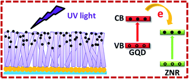
In this communication, we demonstrate a facile method to prepare a graphene quantum dots (GQDs) decorated ZnO nanorod array (ZNRA) ultraviolet detector. The characterization of I–V and time-dependent current behaviors under UV light illumination show that, although GQDs have little influence on the dark conductivity of ZNRA, the coating of GQDs has a remarkable sensitization effect on the photocurrent of ZNRA. This enhancement of the photocurrent was due to the interfacial charge transfer from GQDs to ZNRA.
The challenge in the widespread use of ZnO in photocatalysts, photocurrent and photovoltaic devices is that quick recombination of photo-generated electron–hole pairs occurring in or at the surface results in low quantum efficiency. Therefore, surface modification of ZnO has been developed to promote generation of electron–hole pairs and suppress recombination of photogenerated electron–hole pairs. Noble metals (e.g. Au, Ag and Pt) and metal sulfides (e.g. CdS and ZnS) are usually used to combine with ZnO to form hybrid nanostructure, which leads to improved photocurrent and ultraviolet photoresponse.1–6 Quantum dots (QDs) provide wide-ranging opportunities for harvesting light energy in ultraviolet, visible and infrared regions and show extensive applications in QD solar cells.7,8 Especially, QDs have been widely employed to decorate ZnO for enhancing the photo-generated charge separation and transport to ZnO nanostructures. For example, CdS QDs could improve ultraviolet photoresponse of ZnO film, which derived from suppressed passivation of ZnO film and interfacial carrier transport.9 Furthermore, CdTe QDs displayed a clear photosensitization effect on ZnO ultraviolet sensor due to photoinduced charge transfer from CdTe to ZnO.10 The decorating of QDs on ZnO nanostructures can generate a new interface and enhance charge separation; thereby efficient transfer from QDs to the conduction band of ZnO takes place, which can improve the photoresponse under ultraviolet light radiation. Meantime, QDs (e.g. CdSe, CdS and PbS) as photosensitizers are usually used in photovoltaic devices and photoelectrochemical hydrogen generation applications for efficient charge transfer.11–13 However, considering the high price, limited mineral sources of noble metals, and toxicity of QDs mentioned above, it becomes a serious impediment for large-scale applications. Thus, it is urgent and important to search for the low-cost and eco-friendly new materials to replace the aforementioned nanomaterials, and then further improve the performance of ZnO-based devices. Carbon-based QDs exhibit outstanding properties in photocatalytic and photovoltaic applications. It was reported that carbon QDs loaded on TiO2 NTs improved the light-to-electricity efficiency, also carbon nanoparticles as an interfacial layer between TiO2@ZnO NRAs and conjugated polymers enhanced photocurrent dramatically.14,15 Recently, GQDs, single- or few-layer graphene with a tiny size of only several nanometers, stand for a new type of QDs with the unique properties associated with both graphene and QDs. GQDs have shown a great promise in bio-imaging, photoelectrochemical water splitting, supercapacitors and lithium storage.16–20 The size-dependent band gap and large optical absorptivity of GQDs are particularly interesting for its application as a photosensitizing material in broadband photodetectors and photovoltaic devices.21–23
It was previously reported that ZnO QDs deposited on graphene displayed unique ultraviolet sensing performance due to the high surface to volume ratio of the composite together with high carrier transport and collection efficiency through the graphene.24 Herein, we selected the chemical bath deposition method combined with spin-coating process to fabricate GQDs decorated ZNRA on the interdigital Au electrodes substrates. The optoelectronic behaviors of GQDs coated ZNRA were investigated under ultraviolet light illumination, and the enhanced photocurrent of ZNRA was realized, which attributed to the charge transfer from GQDs to ZNRA.
GQDs were synthesized from graphite oxide (GO) powder by using a facile one-step solvothermal method.19,25 GO powder was prepared from natural graphite powder by a modified Hummers method reported in previous works.26,27 In a typical synthesis, GO powder (1.5 g) was dispersed in 75 ml of N,N-dimethylformamide (DMF) with the aid of ultrasonication 500 W for 1 hour. Then the suspension was transferred to a Teflon-lined autoclave (125 ml) and kept at 200 °C for 8 h. After cooled to room temperature naturally, the mixture was vacuum-filtered. Finally, employing rotary evaporating at reduced pressure, the concentrated GQDs dispersion in DMF was obtained. The preparation process of ZNRA was similar to our previous reports.28,29 GQDs suspension in DMF was spin-coated on the ZNRA to obtain GQDs coated ZNRA. The details of experiments can be seen in ESI.†
Fig. 1 displays typical characterization results of as-prepared GQDs, ZNRA and schematic of decorating process. The transmission electron microscopy (TEM) image (Fig. 1a) exhibits a relatively narrow size distribution of GQDs between 1 and 5 nm with an average diameter of 2.5 nm. Seen from the insert of Fig. 1b, the as-prepared GQDs-DMF solution exhibits a homogeneous phase and no noticeable precipitation can be found even after several months storage at 4 °C. An intense blue-green luminescence of the GQDs-DMF solution under 365 nm light excitation can be found from the inset of Fig. 1b. The optical properties of GQDs in DMF are investigated by UV-vis absorption and PL spectra. It is noteworthy that the UV-vis absorption spectrum of the GQDs shows a typical absorption peak around 240 nm. Moreover, GQDs in DMF displays a broad absorption band below the wavelength of 600 nm. The UV absorption of GQDs is ascribed to the electron transitions from π (or n) to π* of CC, C
N, and C
O.19,22 As seen from PL spectrum in Fig. 1b, the strong luminescence peak centered at 500 nm when excited by light of 365 nm wavelength. The reasons for blue-green light emission are probably attributed to quantum size effect, surface functional groups and defects on GQDs.25 The excitation-dependent PL spectra of GQDs in DMF are also investigated and shown in Fig. S1 (see ESI†). There is an increasing in emission intensity when the excitation wavelength ranges from 280 to 420 nm. And a red shift of the emission peak can be found when the wavelength ranges from 420 to 480 nm, which might be resulted from different emissive sites of GQDs.18,25 Fig. 1c shows the surface morphology of ZNRA, which investigated by scanning electron microscope (SEM). The diameters of ZNRs range from 50 to 100 nm. From the high-resolution TEM image (see Fig. S2 of ESI†), a perfect lattice of pure ZNR is found and the fringe spacing is approximately 0.26 nm corresponding to the d-spacing of (002) plane of hexagonal ZnO, which confirms that the growth of ZNR is along the c-axis direction. Fig. 1d illustrates the decorating process of GQDs on the surface of ZNRA by spin-coating method. GQDs could be deposited on the surface of ZNRs and the interspace among ZNRs. Fig. S3 (see ESI†) is TEM image of sample GQDs coated ZNRA. Although the GQDs are apart from ZNRA during ultrasonication for TEM observation, it confirms successful deposition of GQDs on ZNRA.
The linear–linear plots of the current–voltage characteristics of GQDs coated ZNRA are displayed in Fig. S4 (see ESI†). The linear relationship of current to voltage in range of −6 to 6 V is observed regardless of with/without UV illumination, and it reveals the ohmic contacts. Fig. 2a–e displays the typical current–time characteristics of the ZNRA with/without GQDs decoration at different bias and power density under illumination of 365 nm light. Here, the photosensitivity S of the UV detectors is defined as follows: S = (IUV − Idark)/Idark, where IUV is the current measured under UV illumination, and Idark is current obtained without UV illumination. The photosensitivity S of pure and coated ZNRA can be calculated. There is a remarkable increasing of photosensitivity after coating of GQDs. The photosensitivity of coated ZNRA measured at bias of 5 V is 150 times higher than that of pure ZNRA. Response time can be defined as the time in which the photocurrent increases to 90% of its maximum value. As shown in Fig. 2, it observes that the response time of the pure and coated ZNRA detectors are in the range of 150 to 200 s. In previous reports, the response and recovery times of ZnO nanostructures were in the range of several millisecond to several hours.9,10,30–33 The slow response and recovery times suggest that the photocurrent of the detectors is surface-controlled.30,33 The detector current responsivity is defined as follows: R = (IUV − Idark)/PillA, where Pill is illumination power density and A is effective area of device.34,35 Responsivity of GQDs coated ZNRA with UV illumination of 365 nm light as a function of applied voltage are showed in Fig. S5 (see ESI†). As can be seen in the figure, the responsivity increases linearly with applied bias voltages. Fig. 2e shows the variation in photoresponse of GQDs coated ZNRA as a function of illumination power density of an incident wavelength of 365 nm at 5 V bias. The photoresponse performance of the GQDs coated ZNRA under 254 nm wavelength irradiation is showed in Fig. 2f and it displays good photoresponse performance. The above results indicate that the device is sensitive to UV light regardless of the light energy above or near band gap of ZnO.
In air ambient, absorption and desorption effect of oxygen molecules takes place at the surface of ZNRA and oxygen molecules capture free electrons from ZNRA, which results in charged oxygen ions (O2−) and the depletion layer. The depletion layer decreases the conductivity of ZNRA. When ZNRA illuminated by 254 or 365 nm UV light with the energy above or close to the bang gap of ZnO, the electron–hole pairs generate and photo-generated holes will discharge the O2−. The unpaired electrons accumulate and arrive at the electrodes gradually. The rising of the electrical conductivity of the detector appears until a new equilibrium state of absorption and desorption process reaches. ZnO is a semiconductor with a band gap around 3.3 eV, and its conduction band locates at 4.2–4.4 eV below vacuum level.8,13,16 GQDs have a band gap around 1.5 eV with the conduction band of 3.5–3.7 eV and valence band of 5.1–5.4 eV versus vacuum level.36,37 The location of the conduction band is higher than that of ZnO. Therefore, the photo-generated electrons can transfer from GQDs to ZNRA when UV light is on and the enhanced photocurrent is observed. Fig. 3 displays the band diagram and transfer process of QGDs coated ZNRA. It should be noted that GQDs on ZNRA are partial reduced but have many oxygen-contained functional groups such as C–O, CO, O–C
O bonds. Further, the kind of nitrous C contained in GQDs is different from the precursor GO, which can be found in Fig. S6 and S7 (see ESI†).25,27 After UV light illumination, the GQDs were reduced further, the contents of oxygen- and nitrogen-contained functional groups decreased, which reflected in Fig. S6 and S7 (see ESI†). The functional groups bring defects on GQDs and the further reduction during the UV light illumination causes the structure changes. These will influence the absorption and desorption process of oxygen molecules on the surface of ZNRA and interfacial interactions between GQDs and ZNRA, and affect the photoresponse performance of ZNRA.
![]() | ||
Fig. 3 Schematic band diagram and transfer process of GQDs coated ZNRA. CB and VB represent the conduction and valance bands, respectively. |
In conclusion, GQDs have been deposited on ZNRA using facile spin-coating method. The photocurrent of GQDs coated ZNRA illuminated by UV light is enhanced remarkably compared to that of pure ZNRA. This improvement is probably ascribed to the charge transfer at the interface of GQDs and ZNRA. The facile process proposed here shows a potential route to fabrication of ZnO-based ultraviolet photodetector, and it paves the way for developing GQDs-sensitized efficient optoelectronic devices especially based on other nanostructured photosensitive compounds.
Footnote |
† Electronic supplementary information (ESI) available. See DOI: 10.1039/c5ra07836a |
This journal is © The Royal Society of Chemistry 2015 |