
High dielectric permittivity and low loss tangent of polystyrene incorporated with hydrophobic core–shell copper nanowires
Linxiang He and
Sie Chin Tjong*
Department of Physics and Materials Science, City University of Hong Kong, Hong Kong. E-mail: aptjong@cityu.edu.hk; Fax: +852 34420538; Tel: +852 34427702
First published on 22nd April 2015
Abstract
We reported a low-cost strategy to improve dielectric performance of polystyrene (PS) by incorporating core–shell copper nanowires (CuNWs). The hydrothermally synthesized nanowires had a fresh copper core coated with a hydrophobic insulating layer. Compared with pure PS, CuNW/PS nanocomposites exhibited drastically improved dielectric performance, as manifested by their large dielectric permittivity (ε′) and low loss tangent (tan![[thin space (1/6-em)]](https://www.rsc.org/images/entities/char_2009.gif) δ). At 16 wt% CuNWs loading, dielectric permittivity of the composite reaches 37 at 1 MHz, which was about 14 times larger than that of neat PS (ε′ = 2.5), while the loss tangent of this composite was maintained at a low level (tanδ = 0.04). The pronounced dielectric improvement was ascribed to a large electrical conductivity of the fresh core of CuNWs, which provided the composites with a higher amount of mobile charge carriers participating in the interfacial polarization. The low loss tangent was attributed to the presence of insulating layer on the CuNWs, which impaired the formation of an electrically conductive network, thus suppressing dielectric loss. This simple strategy may open a new avenue to increasing dielectric permittivity of polymers while maintaining relatively low loss tangent.
δ). At 16 wt% CuNWs loading, dielectric permittivity of the composite reaches 37 at 1 MHz, which was about 14 times larger than that of neat PS (ε′ = 2.5), while the loss tangent of this composite was maintained at a low level (tanδ = 0.04). The pronounced dielectric improvement was ascribed to a large electrical conductivity of the fresh core of CuNWs, which provided the composites with a higher amount of mobile charge carriers participating in the interfacial polarization. The low loss tangent was attributed to the presence of insulating layer on the CuNWs, which impaired the formation of an electrically conductive network, thus suppressing dielectric loss. This simple strategy may open a new avenue to increasing dielectric permittivity of polymers while maintaining relatively low loss tangent.
1. Introduction
Polymer nanocomposites with a high dielectric permittivity (high-k) have great potential to store electrical energy and therefore can be used for a broad range of functional applications, such as communication devices, actuators, charge-storage capacitors, etc.1–4 Easy processability of the polymer matrix draws a promising future for these materials.5–7 However, low dielectric permittivity of the polymer matrix still poses a challenge for obtaining high-k polymer composites. Conventional process typically used to increase the dielectric permittivity is by incorporating high-k insulating ceramic fillers into the polymer matrix to form a composite.8–15 To meet the demanding requirements for practical applications, however, a large amount of ceramic fillers is usually required, resulting in a loss of flexibility of the resultant material. Another strategy is to fabricate percolating composites using electrically conductive nanoparticles.16,17 As the content of the nanoparticles grows to the vicinity of the percolation threshold, these composites exhibit an abrupt increase in dielectric permittivity.1,18 It can be several orders of magnitude larger than that of the insulating polymer matrix. This increase is due to an effective increase in the electrode area.19,20 When the content of nanoparticles approaches the percolation threshold, the fillers tend to contact each other but still remain insulated by thin polymer layers, forming a large amount of nanocapacitors with conductive nanoparticles as the electrodes and the polymer matrix as dielectrics.19,21,22 Conductive nanoparticles of large aspect ratios can be employed, resulting in lower percolation thresholds relative to traditional composites.23–27 This strategy also reduces processing costs and maintains material processability.Although polymers incorporated with conductive fillers usually showed large enhancement in dielectric permittivity, high loss tangent often arose due to the formation of a conductive network, thus limiting their practical use as dielectric materials for electrical and electronic devices.17,19,28 To obtain a large dielectric permittivity while ensure a low loss tangent, in this study we used copper nanowires (CuNWs) coated with a hydrophobic insulating layer to enhance the dielectric performance of polymer. This as-synthesized insulating layer served for several purposes: (1) protection of CuNWs from being oxidized; (2) attainment of good dispersion of CuNWs in the polymer matrix; (3) prevention of the formation of a conductive network through the resultant composite, thus suppressing dielectric loss. The resultant polymer nanocomposite displayed high dielectric permittivity, low loss tangent and an appropriate dielectric breakdown strength. Previously, the fabrication and electrical characterization of CuNWs-filled polystyrene (PS) nanocomposites have been well studied.29–35 Thus in this work PS was used as the matrix material because of its compatibility with hydrophobic CuNWs. From the literature, high-k polymer composites have often been obtained by reinforcing polymers with core–shell spherical nanoparticles.36 Little information is available on the preparation and properties characterization of high-k polymer composites with one-dimensional, core–shell metal nanowires.
2. Experimental
Materials
PS pellets were purchased from Dow Chemical Pacific Ltd. Reagent-grade chemicals copper chloride (CuCl2·2H2O, Sigma-Aldrich, 99%), octadecylamine (ODA) (C17H37N, Sigma-Aldrich, 90%), toluene (C7H8, Sigma-Aldrich, 99.7%), ethanol (C2H5OH, Sigma-Aldrich, 99%) and methanol (CH3OH, Sigma-Aldrich, 99%) were used as received without further purification.Synthesis of CuNWs
In a typical process for synthesizing CuNWs, 2 mM ODA was added to 50 mL of copper chloride (20 mM) aqueous solution and stirred overnight. The formed blue emulsion was transferred into an 80 mL Teflon-lined autoclave and kept at 170 °C for 48 h. By cooling the autoclave to room temperature, the supernatant was decanted and the final product was washed with ethanol, methanol and toluene for three cycles. Finally, the product was suspended in toluene.Preparation of CuNW/PS nanocomposites
To prepare CuNW/PS nanocomposite films, PS pellets were firstly dissolved in toluene. It was then mixed with different amounts of CuNWs suspension in toluene. The mixed suspensions were then solution cast and dried to give CuNW/PS films with different CuNW contents. The thickness of the films ranged from 20 to 30 μm. The surface roughness was found to be negligible compared to the film thickness. The films were then fractured in liquid nitrogen for their morphological observations.Characterization
CuNWs were examined in a transmission electron microscope (TEM; Philips FEG CM 20). X-ray diffraction (XRD) patterns of these nanowires were recorded with a Bruker D2 Phaser (Cu tube with λ = 1.54184 Å). Fourier transform infrared (FTIR) spectra were recorded on a Perkin Elmer precisely Spectrum 100 spectrometer. The morphology of CuNWs and the CuNW/PS composites were observed in a scanning electron microscope (SEM; Jeol JSM 820) and field emission scanning electron microscope (FESEM; FEG JSM 6335). The dielectric performance of these composites was measured with an Agilent 4284A Precision LCR Meter. The AC voltage applied was 200 mV. The dielectric permittivity of the composites showed a very weak dependence on the AC voltage. Highly conductive silver ink was coated on the specimen surfaces to form electrodes, and their inductance was neglected. The breakdown strength of the samples was measured in silicon oil at room temperature with a Trek model 609E-6-FG high voltage amplifier under a ramp rate of 200 V s−1. The samples were cut to sizes of 25 cm2.3. Results and discussion
ODA serves as both a reducing agent and a capping agent in the reaction system. It has been well known that long-chain primary amines are mild reducing agent for metal ions.37 ODA has low solubility in water, however, it can dissolve in the aqueous solution of copper chloride. The presence of lone pair of electrons on the nitrogen atom of ODA renders it both basic and nucleophilic. As such, ODA molecules would coordinate with Cu2+ in an aqueous solution. X-ray diffraction (XRD) of the corresponding cast film from the dispersion exhibits periodic peaks (Fig. 1), demonstrating a well-ordered structure. The long spacing (4.15 nm) of the aggregates obtained from the XRD experiments is slightly smaller than twice the evaluated monomolecular length of ODA obtained from the CPK model (2.42 nm), but it is much larger than the monomolecular length, indicating that ODA assembles into bilayer membranes bearing a slightly interdigitation packing model in the CuCl2 solution (Scheme 1). | ||
| Fig. 1 Small angle XRD pattern of cast ODA–CuCl2 film indicating strong interactions between ODA and Cu2+. | ||
 | ||
| Scheme 1 Coordination of ODA to Cu2+ to form Cu(ODA)22+, which acted as a pseudo-double-tailed cationic surfactant and assembled into bilayers through interdigitation, causing the dissolution of ODA in water. | ||
Israelachvili and co-workers proposed the packing parameter concept, i.e. formation of the micelles for single-chain surfactants, and bilayers for double-chain surfactants.38 In the ODA–CuCl2 dispersion, a Cu2+ coordinates with two ODA molecules to form pseudo-double-tailed surfactants with a coordinated headgroup, and then self-assemble into bilayers, causing the dissolution of ODA in CuCl2 solution. In a previous work, Luo et al. reported that ODA also coordinated with Ag+ to form a double-chain surfactant that assembled into bilayers in water.39
The strong interaction of ODA to Cu2+ facilitates electron transfer between them. Under hydrothermal conditions the coordinated electrons were captured by Cu2+, causing a continuous formation of zero-valence copper atoms, which in turn come together to form nuclei (Scheme 2A). Due to the binding of protonized ODA on these nuclei, they would not aggregate into large particles. The subsequent growth of these nuclei resulted in a distribution of multiply twinned, singly twinned, and single-crystal seeds, with the 5-fold twinned decahedron being the lowest in free energy and thus the most abundant morphology (Scheme 2B).40 Consequently, protonized ODA molecules play the role of capping agent such that they adhere to the (100) faces of the seeds (Scheme 2C) and inhibit the growth of these faces, thus direct the growth of these seeds into nanowires (Scheme 2D). A more detailed study of the growth of CuNWs will be given elsewhere.
 | ||
| Scheme 2 Growth process of CuNWs. (A) Nucleation of copper seeds; (B) growth of copper seeds into 5-fold twinned decahedron; (C) selective capping of the newly developed (100) facets by ODA+ bilayers; (D) directed growth of a copper seed into a nanowire. | ||
The synthesized CuNWs can be easily dispersed in nonpolar solvents such as toluene (Fig. 2A) and hexane, but are poorly dispersed in water, indicating their hydrophobic nature. Low magnification SEM image shows that the nanowires are 40–150 nm in diameter, and they have remarkable lengths up to several hundred micrometers (Fig. 2B). The nanowires tend to self-assembly into bundles, as Fig. 2C shows. The diameter of the bundles ranges from several hundred nanometers up to several micrometers. The molar ratio of ODA to CuCl2 is found to play an important role in regulating the morphologies of the products. Excessive ODA would limit the radial growth of the nanowires to a greater degree, thus is helpful for the synthesis of thinner nanowires (Fig. 2C and D). Too much ODA, however, would cap the growing facets of copper nanocrystals and cause the formation of copper nanoparticles (Fig. 2D).
 | ||
| Fig. 2 (A) Stable dispersion of CuNWs in toluene stabilized by PS (10 mg mL−1). (B) SEM micrograph of as synthesized CuNWs. (C) SEM micrograph of two CuNW bundles. Inset: a very thick CuNW bundle with a diameter of 5 μm. (D) SEM micrograph of the mixture of CuNWs, Cu nanoparticles and remnant ODA and/or its derivatives. | ||
The TEM micrographs (Fig. 3) show that the CuNWs are highly flexible and are coated with a thin organic layer. As mentioned above, the binding of protonized ODA to CuNWs resulted in this layer. Due to the hydrophobic nature of this layer, it would trigger hydrophobic–hydrophobic interactions among the nanowires and produce nanowire bundles as shown in Fig. 2C.41 The thickness of the layers ranged from 2 to 8 nm, and it could not be easily removed after several washing cycles, indicating their strong adherence to the CuNWs.
 | ||
| Fig. 3 TEM micrographs of CuNWs at (A) low and (B) high magnifications showing the presence of a surface coating layer. | ||
The insulating layer on the CuNWs can be detected by XRD, as shown in Fig. 4. The weak diffraction of CuNWs at 22.5° corresponds to the ODA peak at about 21°, implying an additional phase of ODA derivatives. The diffraction peaks of CuNWs at 43.2°, 50.4° and 74.1° correspond to the (111), (200) and (220) planes of Cu, respectively. The oxides of copper, such as Cu2O and CuO, are not observed, implying this layer is dense and tightly bind to the CuNWs, thus preventing the permeation of oxygen to the copper core.
 | ||
| Fig. 4 XRD patterns of ODA and the as-synthesized CuNWs. | ||
FTIR spectra obtained from the ODA, cast ODA–CuCl2 film and synthesized CuNWs in the range 2500–3500 cm−1 are shown in Fig. 5. The spectra shows that a prominent feature occurs at 3335 cm−1 in ODA, corresponding to the N–H stretch vibrations from uncoordinated ODA molecules. This feature is completely lost in the ODA–CuCl2 film (curve B), implying that all ODA molecules are coordinated to Cu2+ ions (curve B). This coordination yields three additional modes at 3268 cm−1, 3240 cm−1 and 3157 cm−1 (curve B). Such a shift in the N–H stretch vibration mode on the formation of salts with anions, such as PtCl6−, has been observed in Langmuir–Blodgett films of ODA,42 and ODA-stabilized colloidal gold nanoparticles.43 For CuNWs, the N–H vibrational feature is indiscernible, due to the removal of most ODA derivatives by the washing process. Nonetheless, the methylene anti-symmetric and symmetric vibrations are still observed at 2918 and 2851 cm−1 (curve C), respectively, substantiating the existence of alkyl chains on the CuNWs. The alkyl chains bond to the nanowires via the –NH2+ head group, as in the case of the adsorption of cetyltrimethylammonium headgroup to gold nanorod surfaces.44–46
 | ||
| Fig. 5 FTIR spectra of (A) ODA, (B) cast ODA–CuCl2 film and (C) CuNWs. | ||
The hydrophobic nature of the CuNWs makes them compatible with nonpolar PS. Fig. 6 shows the SEM micrographs of CuNW/PS nanocomposites at different CuNW contents. The porosity in Fig. 6 was caused by the pull-out of CuNWs from the PS matrix during SEM sample preparation. No agglomeration of CuNWs within the composite was observed. The hydrophobic coating layer on the CuNWs enabled them to interact strongly with nonpolar PS molecular chains, causing the nanowires to be effectively disentangled and dispersed. Due to the interaction of PS with them, CuNWs would orient randomly during the solution casting process. It is noted that ODA has also been used to modify other conductive filler materials, such as graphene,47–49 to make it hydrophobic and dispersible in a variety of nonpolar solvents. Fig. 7 shows that the PS tended to crystallize on the nanowires and most CuNWs were located at the center of PS spherulites.
 | ||
| Fig. 6 SEM micrographs of CuNW/PS nanocomposites with different filler weight fractions. (A): 2 wt%; (B): 5 wt%; (C) and (D): 8 wt%. | ||
 | ||
| Fig. 7 SEM micrographs of CuNW/PS nanocomposite showing the crystallization of PS on CuNWs. | ||
The ability of a dielectric material to store energy is mainly related to the polarization of the material, i.e. electric field-induced electric moment in the material, which results in an increase in capacitance. In a dielectric material, four kinds of polarization exist: electronic, atomic, orientational and interfacial polarizations. At lower frequencies all the four types of polarization may contribute but as the frequency increases the orientation and space charge contribution decreases. Hence the relative permittivity gradually decreases as a function of frequency. Polar polymers have permanent dipole moments, thus they generally have a larger dielectric permittivity than nonpolar polymers. For instance, polar polyvinylidene fluoride has a larger dielectric permittivity (ε′ = 8) than nonpolar PS (ε′ = 2.5). At higher frequency, orientation polarization decreases and the electronic and atomic polarizations predominate. For a heterogeneous composite material with different conductivity/dielectric permittivity (σ/ε′) ratio between the matrix and the filler material, interfacial polarization (Maxwell–Wagner–Sillars polarization), also contributes to dielectric permittivity. The interfacial polarization is caused by the discontinuity of the material and generated by the accumulation of charges at the interfaces. It generally occurs at about the same frequency range as orientation polarization. Thus it can be regarded as a large dipole polarization, in which the electric dipole is related to the strength of each charge and the separation between charges. Nanocomposite material generally has a large interfacial region due to the huge surface area of nanofillers. This enables it to accommodate large amount of charges when exposed to an alternate electric field, resulting in a pronounced interfacial polarization.
Fig. 8A shows that the dielectric permittivity of CuNW/PS nanocomposite rises significantly with increasing CuNWs content. At a 16 wt% CuNWs loading, the dielectric permittivity of the composite reaches 37 at 1 MHz, which is about 14 times larger than that of pure PS. In a classic percolation model,50,51 the randomly distributed conductive fillers form clusters (conducting networks) within the insulating matrix. When the size of the largest cluster approaches a critical value, discharge between the electrodes (percolation) happens. The percolation model predicts that the variation of dielectric permittivity with filler content follows a power law relation52
| ε′ = A|pc − p|q | (1) |
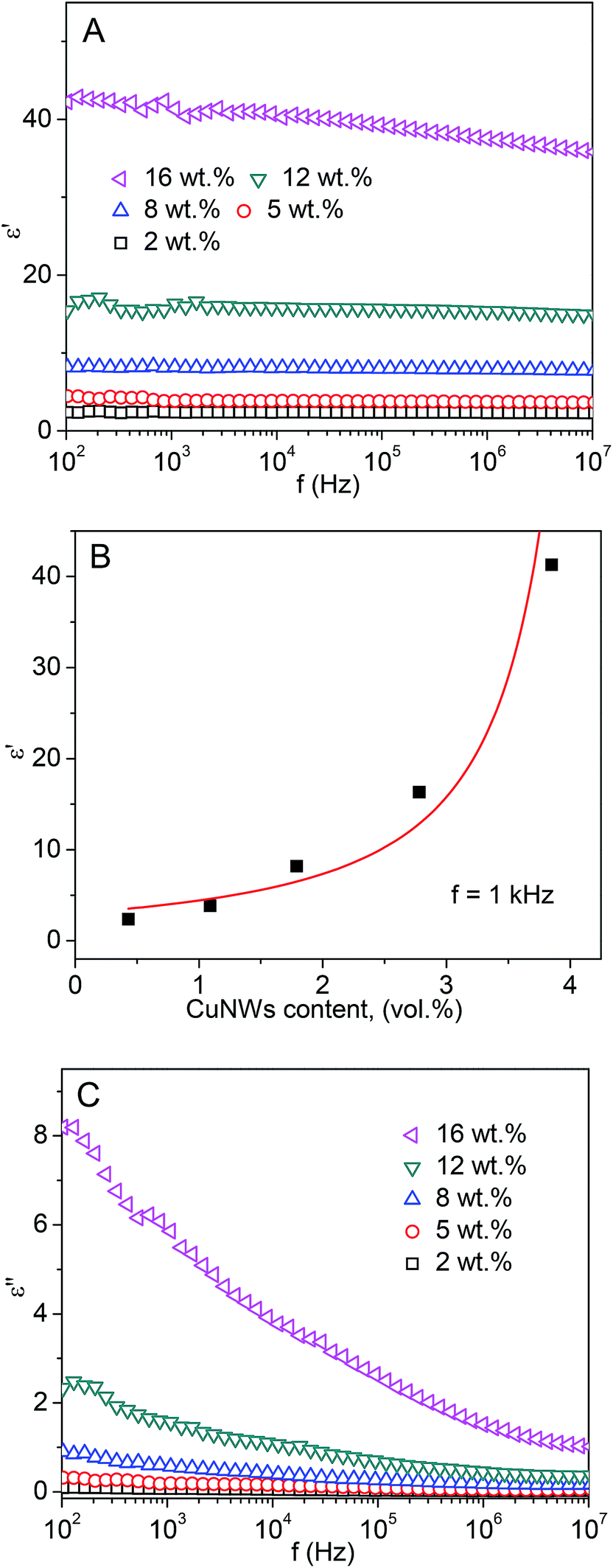 | ||
| Fig. 8 (A) Frequency dependency of real dielectric permittivity of CuNW/PS nanocomposites. (B) The best fit of the 1 kHz ε′ data to eqn (1). The density of the core–shell CuNWs was evaluated to be about 5 g cm−3. (C) Frequency dependency of imaginary dielectric permittivity of CuNW/PS nanocomposites. | ||
Since PS is nonpolar, its dielectric properties show intrinsic weak frequency dependent behavior. By incorporating CuNWs up to 12 wt%, a stable dielectric permittivity over a wide range of frequency is still observed (Fig. 8A). The dielectric permittivity shows weak frequency dependency as the CuNWs content increases to 16 wt%, implying that the interfacial polarization becomes more predominant at high CuNWs loading. Because the relaxation time of interfacial polarization is reversely proportional to the electrical conductivity of the fillers,53 the high conductivity of copper (∼6 × 10⁵ S cm−1) is expected to drastically reduce the relaxation time, allowing the interfacial polarization to respond quickly to the alternating electric field. This indicates that at higher frequency range, where electric field alternates very fast, the charges are still capable of piling up swiftly at the interfacial region, contributing to dielectric permittivity.
Fig. 8C shows the dielectric loss of the CuNW/PS nanocomposites. It can be observed that the dielectric loss rises significantly with CuNWs content. This is attributed to enhanced polarization and ohmic losses. The magnified polarization loss arising from interfacial polarization is a significant factor in producing high dielectric loss at higher filler contents. The decaying trend of dielectric loss with frequency can be ascribed to reduced polarization losses at high frequency. Due to interfacial polarization relaxation, the interfacial charge polarization becomes weaker at high frequency, resulting in lower polarization loss. Moreover, an increase in CuNWs content would reduce the average distance between the nanowires. This would increase the chance of the electrons to tunnel and/or hop between adjacent nanowires in each half cycle of alternating field, thereby leading to conduction loss. Due to the insulating coating layer on the CuNWs, it is proposed that the polarization loss plays a more dominant role.
Both electric dipoles and interfacial polarization try to follow the direction of electric field. The required adjustment period corresponds to the relaxation time of them. The faster the electric field alternates, the longer the orientation lags behind the field and the greater is the electrical energy consumed. Available power output thus decreases because electric power is partly lost by converting into thermal energy. The extent to which the energy is dissipated can be characterized by the dielectric loss tangent (tanδ). The lower the loss tangent of a dielectric material, the better is its performance for charge storage applications. Mathematically, tanδ can be expressed as the ratio of imaginary dielectric permittivity ε′′ to real dielectric permittivity ε′:
| tanδ = ε′′/ε′. |
The loss tangent of an insulating material is of great technological importance, because it quantifies the fraction of energy dissipated in a capacitor. From Fig. 9, the loss tangent of CuNW/PS nanocomposites displays a frequency-dependent behavior. The decaying trend of loss tangent with frequency is a manifestation that interfacial polarization grows weaker at higher frequency. Besides, although the loss tangent of CuNW/PS nanocomposites increases with filler content, it maintains at a relatively low level (<0.04 at 1 MHz) (Fig. 9). The conduction loss mentioned before is linked to the dissipation of energy in phase with an alternating field, and contributes an additional σ/2πfε′ to the loss tangent of the material. Since frequency increase is equivalent to reduced available times for free electrons to travel between the CuNWs in each half cycle of alternating field, it would therefore reduce the conduction loss.
 | ||
| Fig. 9 Frequency dependency of loss tangent of CuNW/PS nanocomposites with different filler contents. The inset shows the loss tangent of CuNW/PS nanocomposites at 1 MHz. | ||
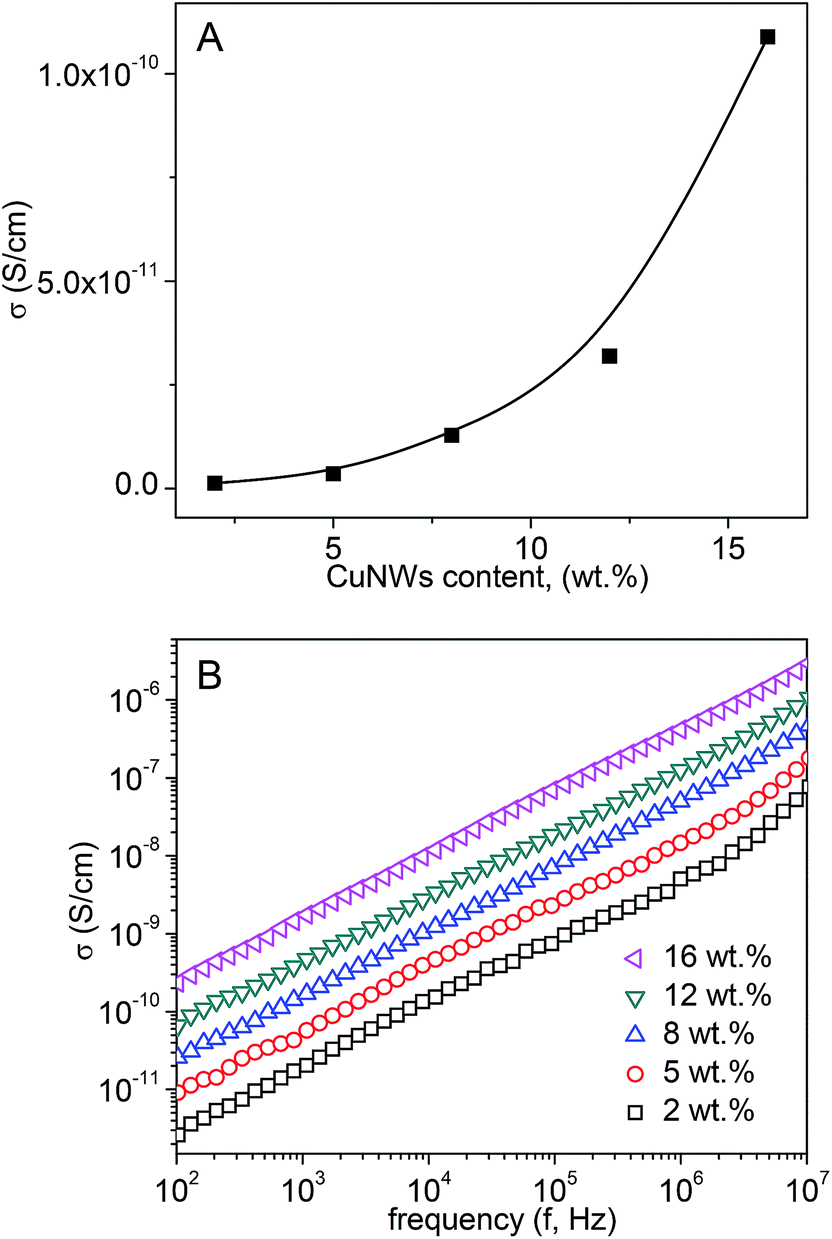
The lower loss tangent of the CuNW/PS nanocomposites is ascribed to the presence of an insulating coating layer on the surface of CuNWs, which impairs the formation of a conductive network at higher CuNWs contents, thus drastically suppressing the conduction loss (σ/2πfε′). Fig. 10A shows the dependency of the 40 Hz conductivity of CuNW/PS composites on the CuNWs content; the linear dependency of conductivity on frequency as shown in Fig. 10B reveals their insulating nature. Therefore, hydrophobic coating layer on the CuNWs cuts the available free path of the nomadic charges and reduces the otherwise possible leaky current. The increase in conductivity with CuNWs contents is due to the increased dissipating charge carriers. As mentioned before, their hopping or tunneling would contribute to the electrical conduction.
 | ||
| Fig. 10 (A) The 40 Hz conductivity and (B) AC conductivity of CuNW/PS nanocomposites at different filler contents. | ||
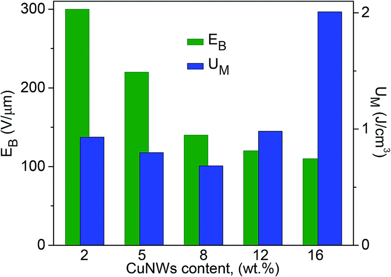
The dielectric breakdown strength (EB) of an insulating material is closely related to its ability to store electrical energy. Fig. 11 gives the dielectric breakdown strength of CuNW/PS nanocomposite with different nanowire contents. Apparently, the breakdown field strength gradually decreases with the increase in CuNWs content, as expected. The maximum energy density (UM) is related to the breakdown strength by the expression: UM = ε0ε′EB2/2 (ε0 = 8.85 × 10⁻¹² F m−1). Fig. 11 shows that UM is rather low (<1 J cm−3) at low filler contents (≤12 wt%), due to the small dielectric permittivity of the material. The drastic increase in UM at 16 wt% content is caused by the large dielectric permittivity (Fig. 8A) and the acceptable low level of EB. An energy density as high as 2 J cm−3 is obtained at a field strength of 300 V μm−1.
 | ||
| Fig. 11 Breakdown field strength and maximum energy density of CuNW/PS nanocomposites at room temperature with different filler contents. | ||
4. Conclusions
In summary, we have presented the synthesis of hydrophobic CuNWs with a core–shell structure and the use of them to improve the dielectric performance of PS. It is demonstrated that the obtained CuNW/PS nanocomposites exhibit large improvement in dielectric permittivity and a relatively low loss tangent. The large dielectric permittivity was caused by the strong interfacial polarization. The low loss tangent was due to the hydrophobic insulating layer on the CuNWs, which averted the direct contact between the nanowires and maintained insulating nature of the resultant composite material. Our method can be potentially used to develop high-k nonpolar polymer nanocomposites for electrical applications.Acknowledgements
This work is supported by the project (R-IND4401), Shenzhen Research Institute, City University of Hong Kong.References
- Z. M. Dang, J. K. Yuan, J. W. Zha, T. Z. Zhou, S. T. Li and G. H. Hu, Prog. Mater. Sci., 2012, 57, 660–723 CrossRef CAS PubMed.
- R. Popielarz, C. K. Chiang, R. Nozaki and J. Obrzut, Macromolecules, 2001, 34, 5910–5915 CrossRef CAS.
- P. Barber, S. Balasubramanian, Y. Anguchamy, S. Gong, A. Wibowo, H. Gao, H. J. Ploehn and H. C. Zur Loye, Materials, 2009, 2, 1697–1733 CrossRef CAS PubMed.
- S. C. Tjong and G. D. Liang, Mater. Chem. Phys., 2006, 100, 1–5 CrossRef CAS PubMed.
- S. C. Tjong and Y. Z. Meng, Eur. Polym. J., 2000, 36, 123–129 CrossRef CAS.
- X. H. Li, S. C. Tjong, Y. Z. Meng and Q. Zhu, J. Polym. Sci., Part B: Polym. Phys., 2003, 41, 1806–1813 CrossRef CAS PubMed.
- K. L. Fung, R. K. Y. Li and S. C. Tjong, J. Appl. Polym. Sci., 2002, 85, 169–176 CrossRef CAS PubMed.
- L. He and S. C. Tjong, Curr. Nanosci., 2010, 6, 40–44 CrossRef CAS.
- Y. Rao, S. Ogitani, P. Kohl and C. P. Wong, J. Appl. Polym. Sci., 2002, 83, 1084–1090 CrossRef CAS PubMed.
- S. Thomas, V. Deepu, S. Uma, P. Mohanan, J. Philip and M. T. Sebastian, Mater. Sci. Eng., B, 2009, 163, 67–75 CrossRef CAS PubMed.
- G. Subodh, V. Deepu, P. Mohanan and M. T. Sebastian, Polym. Eng. Sci., 2009, 49, 1218–1224 CAS.
- S. George, V. Deepu, P. Mohanan and M. T. Sebastian, Polym. Eng. Sci., 2010, 50, 570–576 CAS.
- S. George, P. S. Anjana, M. T. Sebastian, J. Krupka, S. Uma and J. Philip, Int. J. Appl. Ceram. Technol., 2010, 7, 461–474 CAS.
- S. George and M. T. Sebastian, Compos. Sci. Technol., 2009, 69, 1298–1302 CrossRef CAS PubMed.
- A. S. Bhalla, R. E. Newnham, L. E. Cross, W. A. Schulze, J. P. Dougherty and W. A. Smith, Ferroelectrics, 1981, 33, 139–146 CrossRef CAS.
- K. S. Deepa, M. T. Sebastian and J. James, Appl. Phys. Lett., 2007, 91, 202904 CrossRef PubMed.
- K. S. Deepa, S. Kumari Nisha, P. Parameswaran, M. T. Sebastian and J. James, Appl. Phys. Lett., 2009, 94, 142902 CrossRef PubMed.
- S. Wageh, L. He, A. A. Al-Ghamdi, Y. A. Al-Turki and S. C. Tjong, RSC Adv., 2014, 4, 28426–28431 RSC.
- M. J. Jiang, Z. M. Dang, M. Bozlar, F. Miomandre and J. B. Bai, J. Appl. Phys., 2009, 106, 084902 CrossRef PubMed.
- B. E. Kilbride, J. N. Coleman, J. Fraysse, P. Fournet, M. Cadek, A. Drury, S. Hutzler, S. Roth and W. J. Blau, Appl. Phys. Lett., 2002, 92, 4024–4030 CAS.
- M. Arjmand, T. Apperley, M. Okoniewski, U. Sundararaj and S. Park, Carbon, 2012, 50, 5126–5134 CrossRef CAS PubMed.
- G. D. Liang, S. P. Bao and S. C. Tjong, Mater. Sci. Eng., B, 2007, 142, 55–61 CrossRef CAS PubMed.
- L. He and S. C. Tjong, RSC Adv., 2013, 3, 22981–22987 RSC.
- L. He and S. C. Tjong, Nanoscale Res. Lett., 2013, 8, 132 CrossRef PubMed.
- L. He and S. C. Tjong, J. Nanosci. Nanotechnol., 2011, 11, 10668–10672 CrossRef CAS PubMed.
- L. He and S. C. Tjong, J. Nanosci. Nanotechnol., 2011, 11, 3916–3921 CrossRef CAS PubMed.
- L. He and S. C. Tjong, Curr. Nanosci., 2010, 6, 520–524 CrossRef CAS.
- Y. C. Li, S. C. Tjong and R. K. Y. Li, Synth. Met., 2010, 160, 1912–1919 CrossRef CAS PubMed.
- B. Lin, G. A. Gelves, J. A. Haber and U. Sundararaj, Ind. Eng. Chem. Res., 2007, 46, 2481–2487 CrossRef CAS.
- B. Lin, G. A. Gelves, J. A. Haber, P. Pötschke and U. Sundararaj, Macromol. Mater. Eng., 2008, 293, 631–640 CrossRef CAS PubMed.
- G. A. Gelves, B. Lin, J. A. Haber and U. Sundararaj, J. Polym. Sci., Part B: Polym. Phys., 2008, 46, 2064–2078 CrossRef CAS PubMed.
- G. A. Gelves, M. H. Al-Saleh and U. Sundararaj, J. Mater. Chem., 2011, 21, 829–836 RSC.
- G. A. Gelves, B. Lin, U. Sundararaj and J. A. Haber, Nanotechnology, 2008, 19, 215712 CrossRef CAS PubMed.
- M. H. Al-Saleh, G. A. Gelves and U. Sundararaj, Composites, Part A, 2011, 42, 92–97 CrossRef PubMed.
- C. Schmädicke, M. Poetschke, L. D. Renner, L. Baraban, M. Bobeth and G. Cuniberti, RSC Adv., 2014, 4, 46363–46368 RSC.
- X. Huang and P. Jiang, Adv. Mater., 2015, 27, 546–554 CrossRef CAS PubMed.
- D. S. Wang and Y. D. Li, Inorg. Chem., 2011, 50, 5196–5202 CrossRef CAS PubMed.
- J. N. Israelachvili, D. J. Mitchell and B. W. Ninham, J. Chem. Soc., Faraday Trans., 1976, 2, 1525–1568 RSC.
- X. Luo, W. Miao, S. Wu and Y. Liang, Langmuir, 2002, 18, 9611–9612 CrossRef CAS.
- L. D. Marks, Rep. Prog. Phys., 1994, 57, 603–649 CrossRef CAS.
- E. Y. Ye, S. Y. Zhang, S. H. Liu and M. Y. Han, Chem.–Eur. J., 2011, 17, 3074–3077 CrossRef CAS PubMed.
- M. Bardosova, R. H. Tredgold and Z. Ali-Adib, Langmuir, 1995, 11, 1273–1276 CrossRef CAS.
- S. Murali, K. Ashavani and M. Priyabrata, Colloids Surf., A, 2001, 181, 255–259 CrossRef.
- C. J. Murphy, T. K. Sau, A. Gole and C. J. Orendorff, MRS Bull., 2005, 30, 349–355 CrossRef CAS.
- J. Gao, C. M. Bender and C. J. Murphy, Langmuir, 2003, 19, 9065–9070 CrossRef CAS.
- C. J. Murphy, T. K. Sau, A. Gole, C. J. Orendorff, J. Gao, L. Gou, S. Hunyadi and T. Li, J. Phys. Chem. B, 2005, 109, 13857–13870 CrossRef CAS PubMed.
- S. Niyogi, E. Bekyarova, M. E. Itkis, J. L. McWilliams, M. A. Hamon and R. C. Haddon, J. Am. Chem. Soc., 2006, 128, 7720–7721 CrossRef CAS PubMed.
- Y. Cao, J. Feng and P. Wu, Carbon, 2010, 48, 1683–1685 CrossRef CAS PubMed.
- Y. S. Yun, Y. H. Bae, D. H. Kim, J. Y. Lee, I.-J. Chin and H. J. Jin, Carbon, 2011, 49, 3553–3559 CrossRef CAS PubMed.
- S. Kirkpatrick, Rev. Mod. Phys., 1973, 45, 574–588 CrossRef.
- C. W. Nan, Prog. Mater. Sci., 1993, 37, 1–116 CrossRef CAS.
- D. R. Bowman and D. Stroud, Phys. Rev. B: Condens. Matter Mater. Phys., 1989, 40, 4641–4650 CrossRef.
- T. Blythe and D. Bloor, Electrical Properties of Polymers, Cambridge University Press, 2nd edn, 2005 Search PubMed.
| This journal is © The Royal Society of Chemistry 2015 |