Photonic design of embedded dielectric scatterers for dye sensitized solar cells

Mahdi Malekshahi Byranvanda, Ali Dabirian*bc, Ali Nemati Kharata and Nima Taghaviniabd
aSchool of Chemistry, University College of Science, University of Tehran, Tehran, Iran. E-mail: alnema@khayam.ut.ac.ir
bDepartment of Physics, Sharif University of Technology, Tehran 14588, Iran. E-mail: taghavinia@sharif.edu
cPhotovoltaics and Thin Film Electronics Laboratory, Ecole Polytechique Federale de Lausanne (EPFL), Rue de la Maladiere 71, Neuchatel 2002, Switzerland. E-mail: ali.dabirian@epfl.ch; Fax: +41 21 695 42 01; Tel: +41 21 695 42 61
dInstitute for Nanoscience and Nanotechnology, Sharif University of Technology, Tehran 14588, Iran

Received 6th March 2015 , Accepted 31st March 2015

First published on 31st March 2015


Abstract

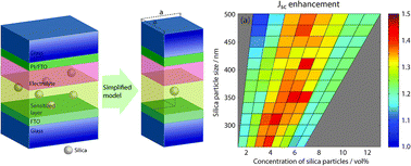
Embedded dielectric scatterers comprise an important approach for light trapping in dye-sensitized solar cells (DSCs) due to their simple fabrication process. The challenge in applying these scatterers lies in finding the optimal dimensions and concentration of the scatterers. This requires many experiments and it is often quite difficult to have a starting point for optimizing the concentration. Based on theories of light propagation in random media, we propose a simple model for DSCs with embedded silica spherical particles. Then, by full-wave optical calculations, we determine a narrow range for the concentration of silica particles that leads to the largest optical absorption in the cell. The simulation results were verified by realizing DSCs with different concentrations of silica particles. A power conversion efficiency of 8.08% in an 11 μm-thick N719-sensitized DSC was achieved with 6 vol% embedded silica, which further increased to 9.30% by applying a white scattering layer on the rear-side of the counter electrode. The design approach, presented here, is a general approach that can be applied for other types of solar light harvesting structures with low optical absorption coefficient.


1. Introduction

Dye sensitized solar cells (DSCs) generally require photon management techniques, in order to compensate for the low optical absorption coefficient of dye molecules.1–3 Back-scattering layers of sub-micron TiO2 particles are conventionally used to reflect the unabsorbed light back into the cell and enhance light harvesting.4–8 These white opaque layers cannot be utilized in transparent DSCs, which are increasingly of interest as energy generating windows, and with the additional function in decorations. Besides, there are DSC structures, such as W-sandwich modules, that light is fully or partly illuminated from back, and therefore an opaque back scattering layer is not suitable.9,10 In these cases the scattering particles need to be embedded into the semi-transparent and mesoporous dye-sensitized TiO2 film, to prolong the light path and increase cell efficiency.11 In this context, voids,12,13 TiO2,14–16 Ag nanowires,17 and SiO2 (ref. 18–20) particles have been used as scattering elements. Compared to other light trapping techniques such as top scattering layer,4–8,21,22 down/up conversion layer,23–27 or photonic crystals,28,29 embedded scatterers do not add any further step in cell fabrication process. This becomes particularly important in scaling up DSC fabrication processes to reduce the production cost.

Size, refractive index, and concentration of embedded scattering particles highly influence the cell performance.11 Therefore to maximize cell efficiency we need to optimize these parameters. For refractive index a simple design rule applies; the larger refractive index contrast of particle with mesoporous TiO2 is, the stronger the scattering is. However for size and concentration of the particles it is difficult to devise design rule and therefore we need to run optimization procedures. In addition, there is a narrow particle concentration window that results in optimum light harvesting. It is known that using large quantity of scatterers leads to blocking the light from entering mesoporous layer, and affects cell's transparency and electron transport.20,30 This emphasizes the importance of optical modelling to predict the optimal size and concentration of scattering particles. Despite extensive studies on this subject and recent significant progress in modelling DSCs as random optical media31,32 there is no empirical solution to obtain a first estimate of the size and the concentration of scattering particles that maximizes cell efficiency.

Here we introduce a simplified model for DSCs with embedded dielectric scatterers that we can rigorously simulate using a full-wave electromagnetic wave solver and then we calculate the overall optical absorption within the cell under air mass 1.5 global (AM1.5G) irradiation with 100 mW cm−2 intensity. We carry out these calculations for a large combination of silica particle sizes and concentrations in the cell and then identify the range for size and concentration of the scatterers leading to maximal optical absorption. Our strategy is to use these theoretically predicted optimal conditions for further experimental optimization. In this way we significantly reduce the number of experiments needed to optimize size and concentration of scatterers. We succeeded in obtaining the optimal concentration of silica spheres in a N719-sensitized cell with accuracy of 1 vol% in only four experiments. We further evaluated the cells performance in inverse configuration, in which light enters into the cell from counter electrode (CE) side. Inverse cell operation is quite important for emerging DSCs applications such as building integrated photovoltaics (BIPV) or transparent PV.33 Moreover, to further improve device performance, we applied a white scattering layer on the rear-side of CE.34,35 The approach we introduce here can also be applied to other sensitized solar absorbers such as organometallic perovskite solar cells,36–38 quantum-dot sensitized solar cells,39,40 and Au nanoparticles sensitized devices for water splitting.41–43

2. Experimental

2.1. Materials

Tetraethyl orthosilicate (TEOS, 98%; Merck), absolute ethanol (C2H6O, 99%; Merck), deionized water (DI water; > 18.2 MΩ), ammonium hydroxide (NH4OH, 25%; Merck), titanium(IV) chloride (TiCl4, > 99%; Merck), standard transparent TiO2 paste (PST-20T, composed of 20 nm TiO2 nanoparticles; Sharif Solar), scatterer anatase TiO2 Paste (PST-300A, composed of 200–300 nm reflector anatase TiO2 particles; Sharif Solar), fluorine-doped tin oxide substrates (FTO; Dyesol), cis-diisothiocyanato-bis(2,2′-bipyridyl-4,4′-dicarboxylato) ruthenium(II) bis(tetrabutylammonium) dye (N719; Dyesol), chloroplatinic acid (H2PtCl6, 99.95%; Merck), Surlyn sheets (60 μm; Dyesol), 1-butyl-3-methylimidazolium iodide (Aldrich), guanidinium thiocyanate (GSCN; Merck), iodine (I2; Merck), lithium iodide (LiI; Merck), 4-tertbutylpyridine (TBP; Merck), acetonitrile (Merck) and valeronitrile (Merck) were used without further purification.

2.2. Synthesis of spherical silica particles

Monodisperse silica particles were synthesized by Stöber method.44 In a typical synthesis, 25 mL of DI water, 62 mL of ethanol, and 9 mL of NH4OH were mixed in a flask and stirred for 30 min till a homogeneous solution was formed. Then 4.5 mL TEOS was rapidly added, then solution was stirred for 3 hours at 20 °C. The white precipitates were centrifuged and washed with absolute ethanol 5 times. The products were dried at 60 °C for 24 hours.

2.3. Preparation of TiO2 paste mixed with silica particles

Different volumes of colloidal solution of silica particles in ethanol were mixed with standard TiO2 paste (PST-20T), dispersed by ultrasonic bath, and then it was stirred for 3 hours. Then ethanol was removed by rotary evaporator.

2.4. Fabrication process of DSCs

FTO substrates were immersed in 40 mM TiCl4 aqueous solution at 70 °C for 30 min and rinsed with DI water and ethanol. Photoanode films were prepared by screen-printing of the paste on TiCl4-treated FTO substrates. Then these films were annealed in air in 3 steps; 325 °C for 5 min, 375 °C for 5 min, and finally 450 °C for 45 min. Photoanode films were treated with 40 mM TiCl4 aqueous solution once more, and then annealed at 500 °C for 30 min. After cooling down, the layers were immersed in N719 dye solution (0.2 mM) overnight, and then rinsed using an acetonitrile solution. CE of 1 cm2 surface area were fabricated by coating FTO substrates with one drop of 5 mM H2PtCl6 ethanolic solution followed by annealing at 450 °C for 15 min.

For certain experiments, anatase TiO2 scattering paste (PST-300A) containing 200–300 nm particles was screen-printed onto the rear-side of an FTO glass. Nearly 10 μm-thick scattering layers were deposited by multiple screen-printing steps. The layers were dried between successive screen printing steps at 120 °C for 5 minutes. Finally the scattering layers were sintered at 500 °C for 30 min. Pt deposition was conducted on the FTO side as explained and then the cell was encapsulated using this electrode and then the electrolyte was injected.

Dye-sensitized photoanodes were assembled with Pt CE (with a drilled hole) into sandwich-type cell by heating at 120 °C using a hot-melt film (Surlyn) as the spacer between the electrodes. A drop of electrolyte solution was placed on the hole in CE and it was driven into the cell via vacuum backfilling. The electrolyte solution contains 1.0 M 1-butyl-3-methylimidazolium iodide, 0.03 M I2, 0.05 M LiI, 0.1 M GSCN and 0.5 M TBP in acetonitrile and valeronitrile solvent mixture (85[thin space (1/6-em)]:[thin space (1/6-em)]15 volumetric ratio). Finally, the hole was sealed using additional Surlyn and a cover glass.

2.5. Characterization

Scanning electron microscopy (SEM) was carried out using a Tescan (Czech Republic) Vega II XMU microscope. Diffuse reflection, transmittance, and absorptance measurements were carried out using an Avantes photospectrometer (Avaspec-2048TEC) equipped with an integrating sphere. Current–voltage plots were recorded using a Palmsens potentiostat under simulated AM1.5G light (Sharif Solar). Incident photon to current conversion efficiency (IPCE), measured using a setup consisting of a Jarrel-Ash monochromator, a 100 W halogen lamp and a calibrated photodiode (Thorlabs). Dye loading on mesoporous TiO2 films was measured by desorption of dye through soaking dye-sensitized TiO2 films in 0.1 M NaOH aqueous solution. Concentration of desorbed dyes was estimated from optical absorption of the 0.1 M NaOH aqueous solution containing the desorbed dye molecules.

3. Results and discussion

Fig. 1a shows the schematic of a DSC with silica particles randomly distributed within the mesoporous TiO2 layer. It is extremely complicated to model this device using classical electrodynamics approaches because of the random position of scatterers within the dye-sensitized layer. However since the physical phenomena taking place in random media, i.e. multiple scattering and light localization, are similar to those occurring in periodic media therefore it is possible to approximate the random media with an equivalent periodic media.45,46 In principle random media can be understood as a periodic medium with a lattice constant approaching infinity.45 Therefore we develop an equivalent periodic model for the dye sensitized layer with randomly distributed silica particles.
image file: c5ra04020e-f1.tif
Fig. 1 (a) Schematic of a DSC with embedded silica particles. (b) A unit cell of the simplified model for DSC in part (a) that was used in optical simulations.

In developing the equivalent model of DSC we apply the following simplifications to cell structure: (i) an equivalent complex refractive index is obtained for the dye-sensitized layer using the experimentally reported data through effective medium theory.47–49 (ii) Silica particles are considered as perfect spherical dielectric objects with diameters varied in a specific range and they are inserted exactly in middle of the dye-sensitized layer. This is an accurate approximation for silica particles properly synthesized in a Stöber process44 because the particles can be synthesized with narrow size distribution and nearly ideal spherical shape. (iii) Thickness of the sensitized layer is fixed such that there would be always a distance larger than one wavelength (in mesoporous TiO2 layer with refractive index of 1.9) between the particle and interfaces of dye-sensitized layer with either electrolyte or FTO. In this way, we prevent our modelling to be subjected to subwavelength effects that may occur due to small distance between silica particles and each of the interfaces.50 We are aware that in an actual DSC device there are particles with subwavelength distances from the interfaces but population of these events is negligible especially in a mesoporous matrix.

The parameters of the equivalent periodic structure, i.e. lattice constant a and particles dimensions are obtained from the concentration of scattering particles in the medium and the average size of scattering particles, respectively. Basically we choose the lattice constant so that in the equivalent periodic structure there will be a concentration of silica particles identical to that of the actual random structure. Then in our optimization process, we independently vary the size of silica particle and the lateral dimensions of the unit cell, i.e. a in Fig. 1b, keeping thickness of the sensitized layer fixed. We basically tune the concentration through adjustment of lattice constant.

Scattered light from silica particles is subject to secondary scattering from the planar interfaces in the cell and/or from other silica particles in the layers, which is called multiple scattering. The simplified model of the cell, considered here, takes this effect into account because still multiple scattering can occur because of the planar interfaces in the cells as well as other silica particles in the lattice. Here in our modelling we have neglected the multiple scattering effect in which scattered light from one particle directly interact with another particle before reaching the interfaces. This effect could be significant in high concentration of scattering particles51 however in light trapping in DSCs we do not approach those concentrations because dye adsorption and hence optical absorption will be significantly reduced. In addition, highly scattering media are not suitable for light localization due to their large optical backscattering.52

We model sunlight interaction with DSC by solving full-wave Maxwell equation over the entire simplified DSC structure of Fig. 1b using a rigorous coupled-mode approach (RCWA).47,53,54 Full-wave modelling means that we take into account the multiple scattering as well as radiating and evanescent fields. Sunlight illumination was modelled as single–frequency plane wave, perpendicularly irradiated on DSC from the FTO side, which is the default configuration for DSC operation. Wavelength of incident plane wave was varied from 350 nm to 800 nm to account for the broad spectrum of sunlight that is absorbed by a N719-sensitized TiO2 layer. From RCWA calculations we obtained electromagnetic fields over the entire structure and from these data we calculated optical absorption in the sensitized layer as described previously.47 In the next step, we calculate AM1.5G integrated optical absorption, JSCT, of the cells which basically is the maximum photocurrent density that can be obtained from DSC under AM1.5G illumination. JSCT is equivalent to short circuit current density of the actual solar cell device with 100% charge collection efficiency, defined as image file: c5ra04020e-t1.tif, where A(λ) is the optical absorptance of the layer, and ϕAM1.5(λ) is irradiation spectrum of AM1.5G.

Fig. 2a shows the enhancement in calculated JSCT values for DSC with embedded silica particles relative to similar DSC without the scatterers as concentration and size of silica particles vary. We varied silica particle size from 200 nm to 500 nm and kept the layer thickness fixed at 2 μm. The reason for choosing 2 μm is that this thickness is large enough for the 500 nm particle dimension we study here so that there would be always a distance larger than one wavelength between the particle and interfaces of N719-sensitized layer with either electrolyte or FTO.


image file: c5ra04020e-f2.tif
Fig. 2 (a) Enhancement is integrated optical absorption, JSCT, of DSC with embedded silica particles relative to JSCT of a similar DSC without silica particles (T) plotted versus concentration (volume percentage) and size of silica particles. (b) Optical absorptance spectra of a reference 2 μm-thick cell and the same cell with different concentrations of 450 nm silica spheres.

In our calculations, for every silica particle size, we varied unit cell dimension from silica particle size to particle size multiplied by 5 in 9 steps. For instance, for a 450 nm silica particle the lattice constant is varied from 450 nm to 2250 nm. This variation gives a range of variation in volume fraction (concentration) of silica particles. Therefore graph of Fig. 2a, for every silica particle size, gives a range of concentrations that maximizes optical absorption enhancement. For instance for a 450 nm particle size a concentration of 4 to 8 vol% gives an optimal JSCT enhancement. We use this range as the base for our experimental optimization of silica particles in DSC.

Fig. 2b shows the absorptance spectra calculated for cell without silica particles, and cells with 4, 6, and 9 vol% of 450 nm silica particles. Presence of scatterers improves the optical absorptance over the entire wavelength range of 350–800 nm. This enhancement is more pronounced for 6 vol% concentration of silica particles. The sharp peaks observed at longer wavelengths are the Floquet–Bloch modes, which are the artefacts of periodic approximation made for the cells.45,46 Contribution of these peaks to JSCT is negligible because they have a narrow bandwidth.47

Nearly monodisperse silica particles were synthesized in a Stöber process at 20 °C for 3 hours which gave particles of about 450 nm shown in Fig. 3a. These particles were mixed in a standard transparent TiO2 paste (PST-20T) giving a final concentration of 5, 6, 7, and 8 vol% silica particles in the paste. Top-view and side-view SEM pictures of 6 vol% silica particles embedded in the mesoporous layer are shown in Fig. 3b–d illustrating that silica particles are uniformly mixed in the paste and no aggregation of silica particles takes place. Thickness of the layers was estimated from the SEM image to be nearly 11 μm (ESI, Fig. S1). The layers were obtained by a five-step of screen printing process. The electrodes were sensitized with N719 dye and then the cells were built using liquid iodide electrolyte, and Pt counter electrode. A reference cell, designated as T in the data, was also built with identical features but without any silica particle.


image file: c5ra04020e-f3.tif
Fig. 3 SEM pictures of (a) silica particles, (b and c) 6 vol% of silica particles embedded in the mesoporous TiO2 layer from the top and (d) from the side.

The cells' photovoltaic data, measured under simulated AM1.5G illumination by masking a 25 mm2 area of the cell, are summarized in Table 1 where the efficiency is calculated from η = JSC × VOC × FF. Fig. 4a shows the JV curves of cells fabricated with different concentration of scatterers and also of reference DSC (T) with the same thickness but without any silica particle. Maximum power conversion efficiency (η) of 8.08% was obtained with 6 vol% of silica particles in the sensitized layer. This shows 27% improvement in cell efficiency relative to reference cell (T) with 6.36% efficiency. Further increase or decrease in concentration of silica particles does not lead to improvement in efficiency. This confirms the robustness of simplified model combined with full-wave electromagnetic solver in providing a narrow range for searching optimal concentration of silica particles.

Table 1 Photovoltaic data of DSCs processed with and without silica particles
Device JSC [mA cm−2] VOC [V] FF [%] η [%]
T (no silica) 12.52 0.744 68.3 6.36
5 vol% Silica particles 15.68 0.739 65.4 7.53
6 vol% Silica particles 16.56 0.744 65.6 8.08
7 vol% Silica particles 15.62 0.738 65.4 7.49
8 vol% Silica particles 15.06 0.739 65.4 7.23


image file: c5ra04020e-f4.tif
Fig. 4 (a) Photocurrent density versus voltage (JV) curves, (b) IPCE, and IPCE enhancement spectra for DSCs with different concentrations of silica particles. IPCE enhancement (light blue curve) is defined as IPCE6 vol%(λ)/IPCET(λ), where IPCE6 vol%(λ) and IPCET(λ) are the IPCEs of DSCs with 6 vol% silica particles and without silica particles at wavelength λ, respectively.

Efficiency improvement of the cell is largely due to improvement in short circuit current density (JSC) whereas open-circuit voltage (VOC) does not change and fill-factor (FF) slightly deteriorates. The reference cell gives JSC = 12.52 mA cm−2, which is increased by 32%, reaching 16.52 mA cm−2 in DSC with 6 vol% silica particles in its sensitized layer. This 32% JSC enhancement is quiet close to the 38% that has been theoretically predicted (Fig. 2a). We should mention that reproducibility in thickness of our DSCs is 95%. This extra 5% thickness would alter the reference cell JSC by less than 0.5 mA cm−2, which is significantly smaller than the extra 4 mA cm−2 that is obtained by adding 6 vol% silica particles.

Fill-factor of the cells with scatterers is slightly smaller than the reference cell but among different concentrations of silica particles FF is not significantly influenced. Slight deterioration in FF after addition of silica particles is expected because presence of these insulating silica particles slightly perturbs electronic transport through the sensitized layer.20,30

JSC is related to incident photon-to-electron conversion efficiency (IPCE) through image file: c5ra04020e-t2.tif, therefore the positive effect of silica particles is expected to be pronounced in IPCE too. Fig. 4b shows the IPCE spectra of DSCs with different concentrations of silica particles, IPCE of the reference cell, and the enhancement in the IPCE of the cell with 6 vol% silica particles relative to reference cell. Presence of silica particles improves IPCE over the entire wavelength range with a stronger improvement taking place in the longer wavelength range where optical absorption coefficient of N719-sensitized layer is weak. This effect is made better visible in IPCE enhancement spectra where the enhancement is more pronounced at λ > 700 nm.

Optical absorbance (−log(transmittance)) spectra, depicted in Fig. 5, show a trend with concentration of silica particles similar to that of IPCE because IPCE is directly related to optical absorption. This graph reconfirms that broadband optical absorption enhancement in the layer is provided by adding silica particles. In addition the layer with 6 vol% of silica particles clearly shows the largest optical absorbance among all different concentrations. This observation further confirms that improvement in cells efficiency, by applying silica particles, is largely due to enhanced optical absorption, which is provided as the result of improved light trapping in sensitized layer caused by silica particles.


image file: c5ra04020e-f5.tif
Fig. 5 Optical absorbance (−log(transmittance)) spectra of DSCs with different concentrations of silica particles in N719-sensitized layer of 11 μm.

The enhancement in near infrared wavelength is not clearly visible in this graph because the absorbance values are very small due to logarithmic nature of an absorbance. Instrumentally it is very difficult to make the improvement in small absorbance range visible due to limited accuracy of UV-vis spectrometers.

We further explored the potential of cells with optimal 6 vol% silica particles by evaluating their performance in inverse configuration (Fig. 6b). Table 2 summarizes photovoltaic data of the cell with 6 vol% of silica particles in different configurations. In inverse operation the efficiency of reference cell drops by 28.8% whereas the drop in efficiency of cell with 6 vol% is 23.7%. Therefore the presence of silica particles slightly improves cell performance in inverse configuration.


image file: c5ra04020e-f6.tif
Fig. 6 (a–c) Schematics showing three different configurations of DSC photovoltaic evaluations. (d) JV data of reference cell and cell with optimal 6 vol% silica particles measured in normal configuration (a) inverse configuration (b), and in normal configuration but with a thick scattering layer applied to rear of CE (c), which is labelled as exterior scatterer.
Table 2 Photovoltaic data of reference cell and cell with optimal 6 vol% silica particles in normal and inverse operation, and also when an exterior scattering layer is applied to the rear side of CE. Schematic of these configurations is shown in Fig. 6a–c
Device JSC [mA cm−2] VOC [V] FF [%] η [%]
T (no silica) 12.52 0.744 68.3 6.36
T (no silica)/inverse cell 8.94 0.739 68.8 4.54
T (no silica)/exterior scatterer 15.49 0.739 66.3 7.59
6 vol% Silica particles 16.56 0.744 65.6 8.08
6 vol% Silica particles/inverse cell 12.94 0.744 64.9 6.24
6 vol% Silica particles/exterior scatterer 19.34 0.744 64.6 9.30


The efficiency of the cells was further improved by applying a white scattering layer on the rear side of CE (Fig. 6c). A thick scattering layer of 200–300 nm anatase TiO2 particles (PST-300A) was screen-printed on rear-side of CE. Presence of this layer improved the efficiencies of the reference cell to 7.59% and the efficiency of the cell with 6 vol% silica particles to 9.30% (Table 2). This highlights an important feature of light trapping by embedded scatterers; i.e. cell transparency, which still allows using other light trapping methods like scattering layer to further enhance the efficiency.

IPCE spectra of these cells (ESI, Fig. S5) shows that in inverse configuration the deterioration in cell performance takes place over the entire spectrum, presumably due to dissipation by the Pt layer as well as the electrolyte. Addition of the scattering layer on the rear side of CE enhances the performance over the entire wavelength as is expected with such scattering layers.

4. Conclusion

We have developed a model for DSCs with embedded silica particles to estimate the optimal size and concentration of scattering particles and we showed experimentally that the modelling results provide a reasonably accurate starting point for experimental optimization. This model significantly reduces the experimental resources required to optimize size and concentration of embedded scattering particles. Power conversion efficiency of the cell with no silica particles was improved from 6.36% to 8.08% after adding 6 vol% of 450 nm silica particles. The efficiency was reached 9.30% after applying a standard anatase TiO2 scattering layer on the rear-side of CE. Another advantage of using embedded silica particles is that the cells operate better in inverse operation in which the cell is illuminated from the CE which is an important advantage for BIPV applications. In a broader context the approach we have taken here for optimizing concentration of scattering particles is a general approach that can be applied to other systems like quantum dot sensitized solar cells.

Notes and references

  1. B. O'Regan and M. Grätzel, Nature, 1991, 353, 737–740 CrossRef.
  2. Q. Zhang and G. Cao, Nano Today, 2011, 6, 91–109 CrossRef CAS PubMed.
  3. B. E. Hardin, H. J. Snaith and M. D. McGehee, Nat. Photonics, 2012, 6, 162–169 CrossRef CAS.
  4. F. Lv, S. Xiao, J. Zhu and H. Li, RSC Adv., 2014, 4, 36206–36211 RSC.
  5. J. Liang, G. Zhang, H. Xia and W. Sun, RSC Adv., 2014, 4, 12649–12652 RSC.
  6. F. Shao, J. Sun, L. Gao, S. Yang and J. Luo, ACS Appl. Mater. Interfaces, 2011, 3, 2148–2153 CAS.
  7. S. Ito, P. Chen, P. Comte, M. K. Nazeeruddin, P. Liska, P. Péchy and M. Grätzel, Progress in Photovoltaics: Research and Applications, 2007, 15, 603–612 CrossRef CAS.
  8. J.-J. Wu, W.-P. Liao and M. Yoshimura, Nano Energy, 2013, 2, 1354–1372 CrossRef CAS PubMed.
  9. G. Hashmi, K. Miettunen, T. Peltola, J. Halme, I. Asghar, K. Aitola, M. Toivola and P. Lund, Renewable Sustainable Energy Rev., 2011, 15, 3717–3732 CrossRef CAS PubMed.
  10. A. Fakharuddin, R. Jose, T. M. Brown, F. Fabregat-Santiago and J. Bisquert, Energy Environ. Sci., 2014, 7, 3952–3981 CAS.
  11. Q. Zhang, D. Myers, J. Lan, S. A. Jenekhe and G. Cao, Phys. Chem. Chem. Phys., 2012, 14, 14982–14998 RSC.
  12. T. T. Trang Pham, T. Bessho, N. Mathews, S. M. Zakeeruddin, Y. M. Lam, S. Mhaisalkar and M. Grätzel, J. Mater. Chem., 2012, 22, 16201–16204 RSC.
  13. S. Hore, P. Nitz, C. Vetter, C. Prahl, M. Niggemann and R. Kern, Chem. Commun., 2005, 2011–2013 RSC.
  14. C. J. Barbé, F. Arendse, P. Comte, M. Jirousek, F. Lenzmann, V. Shklover and M. Grätzel, J. Am. Ceram. Soc., 1997, 80, 3157–3171 CrossRef PubMed.
  15. B. Tan and Y. Wu, J. Phys. Chem. B, 2006, 110, 15932–15938 CrossRef CAS PubMed.
  16. Y. Bai, Z. Xing, H. Yu, Z. Li, R. Amal and L. Wang, ACS Appl. Mater. Interfaces, 2013, 5, 12058–12065 CAS.
  17. H. Dong, Z. Wu, F. Lu, Y. Gao, A. El-Shafei, B. Jiao, S. Ning and X. Hou, Nano Energy, 2014, 10, 181–191 CrossRef CAS PubMed.
  18. J.-W. Choi, H. Kang, M. Lee, J. S. Kang, S. Kyeong, J.-K. Yang, J. Kim, D. H. Jeong, Y.-S. Lee and Y.-E. Sung, RSC Adv., 2014, 4, 19851–19855 RSC.
  19. J. T. Park, J. H. Prosser, S. H. Ahn, S. J. Kim, J. H. Kim and D. Lee, Adv. Funct. Mater., 2013, 23, 2193–2200 CrossRef CAS.
  20. Y. Rho, M. Wanit, J. Yeo, S. Hong, S. Han, J. H. Choi, W. H. Hong, D. Lee and S. H. Ko, J. Phys. D: Appl. Phys., 2012, 46, 48 Search PubMed.
  21. N. Ghazyani, M. H. Majles Ara, F. Tajabadi, A. Dabirian, R. Mohammadpour and N. Taghavinia, RSC Adv., 2014, 4, 3621–3626 RSC.
  22. S. Dadgostar, F. Tajabadi and N. Taghavinia, ACS Appl. Mater. Interfaces, 2012, 4, 2964–2968 CAS.
  23. L. Liang, Y. Lin and X. Z. Zhao, Chem. Commun., 2013, 49, 3958–3960 RSC.
  24. G. Zhu, X. Wang, H. Li, L. Pan, H. Sun, X. Liu, T. Lv and Z. Sun, Chem. Commun., 2012, 48, 958–960 RSC.
  25. M. J. Lim, Y. N. Ko, Y. Chan Kang and K. Y. Jung, RSC Adv., 2014, 4, 10039–10042 RSC.
  26. Z. Hosseini, E. W.-G. Diau, K. Mehrany and N. Taghavinia, ChemPhysChem, 2014, 15, 3791–3799 CrossRef CAS PubMed.
  27. Z. Hosseini, W. K. Huang, C. M. Tsai, T. M. Chen, N. Taghavinia and E. W. G. Diau, ACS Appl. Mater. Interfaces, 2013, 5, 5397–5402 CAS.
  28. S. Guldin, S. Hüttner, M. Kolle, M. E. Welland, P. Müller-Buschbaum, R. H. Friend, U. Steiner and N. Tétreault, Nano Lett., 2010, 10, 2303–2309 CrossRef CAS PubMed.
  29. S. Y. Heo, J. K. Koh, G. Kang, S. H. Ahn, W. S. Chi, K. Kim and J. H. Kim, Adv. Energy Mater., 2014, 4, 1300632 Search PubMed.
  30. S.-J. Ha and J. H. Moon, Sci. Rep., 2014, 4, 5375 CAS.
  31. F. E. Gálvez, P. R. F. Barnes, J. Halme and H. Míguez, Energy Environ. Sci., 2014, 7, 689–697 Search PubMed.
  32. F. E. Gálvez, E. Kemppainen, H. Míguez and J. Halme, J. Phys. Chem. C, 2012, 116, 11426–11433 Search PubMed.
  33. S. Zhang, X. Yang, Y. Numata and L. Han, Energy Environ. Sci., 2013, 6, 1443–1464 CAS.
  34. Q. Xu, F. Liu, Y. Liu, K. Cui, X. Feng, W. Zhang and Y. Huang, Sci. Rep., 2013, 3, 2112 Search PubMed.
  35. J. Y. Lee, S. Lee, J. K. Park, Y. Jun, Y. G. Lee, K. M. Kim, J. H. Yun and K. Y. Cho, Opt. Express, 2010, 18, A522–A527 CrossRef CAS PubMed.
  36. A. Kojima, K. Teshima, Y. Shirai and T. Miyasaka, J. Am. Chem. Soc., 2009, 131, 6050–6051 CrossRef CAS PubMed.
  37. W. Zhang, M. Saliba, S. D. Stranks, Y. Sun, X. Shi, U. Wiesner and H. J. Snaith, Nano Lett., 2013, 13, 4505–4510 CrossRef CAS PubMed.
  38. J. Burschka, N. Pellet, S.-J. Moon, R. Humphry-Baker, P. Gao, M. K. Nazeeruddin and M. Grätzel, Nature, 2013, 499, 316–319 CrossRef CAS PubMed.
  39. J. S. Niezgoda, E. Yap, J. D. Keene, J. R. McBride and S. J. Rosenthal, Nano Lett., 2014, 14, 3262–3269 CrossRef CAS PubMed.
  40. S. Buhbut, S. Itzhakov, I. Hod, D. Oron and A. Zaban, Nano Lett., 2013, 13, 4456–4461 CrossRef CAS PubMed.
  41. C. Clavero, Nat. Photonics, 2014, 8, 95–103 CrossRef CAS.
  42. F. Su, T. Wang, R. Lv, J. Zhang, P. Zhang, J. Lu and J. Gong, Nanoscale, 2013, 5, 9001–9009 RSC.
  43. Z. Zhang, L. Zhang, M. N. Hedhili, H. Zhang and P. Wang, Nano Lett., 2013, 13, 14–20 CrossRef CAS PubMed.
  44. W. Stöber, A. Fink and E. Bohn, J. Colloid Interface Sci., 1968, 26, 62–69 CrossRef.
  45. Z. Yu, A. Raman and S. Fan, Proc. Natl. Acad. Sci. U. S. A., 2010, 107, 17491–17496 CrossRef CAS PubMed.
  46. P. W. Anderson, Phys. Rev., 1958, 109, 1492–1505 CrossRef CAS.
  47. A. Dabirian and N. Taghavinia, RSC Adv., 2013, 3, 25417–25422 RSC.
  48. S. Foster and S. John, Energy Environ. Sci., 2013, 6, 2972–2983 CAS.
  49. S. Wenger, M. Schmid, G. Rothenberger, A. Gentsch, M. Grätzel and J. r. O. Schumacher, J. Phys. Chem. C, 2011, 115, 10218–10229 CAS.
  50. V. R. Almeida, Q. Xu, C. A. Barrios and M. Lipson, Opt. Lett., 2004, 29, 1209–1211 CrossRef.
  51. D. S. Wiersma, P. Bartolini, A. Lagendijk and R. Righini, Nature, 1997, 390, 671–673 CrossRef CAS PubMed.
  52. M. B. Van Der Mark, M. P. Van Albada and A. Lagendijk, Phys. Rev. B: Condens. Matter Mater. Phys., 1988, 37, 3575–3592 CrossRef.
  53. A. Dabirian, J. Opt., 2014, 16, 075001 CrossRef.
  54. A. Dabirian, M. Akbari and N. A. Mortensen, J. Opt. A: Pure Appl. Opt., 2005, 7, 663–668 CrossRef.

Footnote

Electronic supplementary information (ESI) available: Side-view SEM image to estimate layer thickness, diffuse reflectance and diffuse transmittance spectra of the layers, digital photographs of films, and dye loading data. See DOI: 10.1039/c5ra04020e

This journal is © The Royal Society of Chemistry 2015
Click here to see how this site uses Cookies. View our privacy policy here.