Enhanced output-power of nanogenerator by modifying PDMS film with lateral ZnO nanotubes and Ag nanowires

Xule Yue, Yi Xi*, Chenguo Hu, Xianming He, Shuge Dai, Lu Cheng and Guo Wang
Department of Applied Physics, Chongqing University, Chongqing, 400044, China. E-mail: yxi6@cqu.edu.cn; Fax: +86 23 65678362; Tel: +86 23 65678362

Received 7th February 2015 , Accepted 25th March 2015

First published on 25th March 2015


Abstract

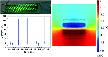
In this paper, a nanogenerator based on flexible polydimethylsiloxane (PDMS) film modified with semiconductor zinc-oxide (ZnO) nanotubes and conductive Ag nanowires is designed and fabricated. The modified PDMS film consists of semiconductor ZnO nanotubes distributed on a dielectric PDMS film with conductive Ag nanowires covered on the surface of the ZnO nanotubes and another thin PDMS layer encapsulated on the top, which forms the structure of PDMS/Ag/ZnO/PDMS. The Ag nanowires act as multi-antennal electrodes and play an important role in improvement of output power. The performance of the nanogenerator with different modified PDMS films is investigated under different measurement conditions. The output current density and power density of the generator under periodic stress (20 N) are 10 μA cm and 1.1 mW cm−2, respectively. The instantaneous output current peak can reach as high as 115 μA (23.75 μA cm−2) under a pressure of 90 N which can be used to light up 99 commercial green LEDs connected in series. The output power of this modified PDMS-based nanogenerator is much higher than that of previously reported PDMS-based nanogenerators, demonstrating excellent structural advantages.

1. Introduction

The energy crisis and global warming are two major worldwide problems that human beings are facing. This situation creates a great need for developing renewable energy sources such as wind,1 solar,2 biomass,3 hydro,4 tidal energy,5 and so on. However, these traditional energy harvesting methods are greatly influenced by environmental factors and normally take up much space. We usually ignore other ubiquitously available energy (such as body movement, irregular airflow/vibration, automobile exhaust, etc.) in our living environment. It is wonderful to harvest this scattered but abundant energy to drive small electronics, for example mobile phones. A nanodevice for harvesting ambient irregular energy is known as a nanogenerator (NG).

Since Professor Wang reported a piezoelectric nanogenerator based on ZnO nanowires (NWs) arrays in 2006 for the first time,6 nanogenerators (NG) have attracted great attention around the world. Outstanding progress has been made in developing PDMS-based NGs with different materials such as ZnO nanoparticles,7 PZT nanofibers,8 BaTiO3 thin film,9 ZnO nanorod arrays10 and so on. However, the output current and output power of these devices are relatively low, and this insufficient power output probably limits their practical application. Therefore, improvement of the output current and power is a significant and challenging task.

In this paper, we design a NG based on modified PDMS with a PDMS/Ag/ZnO/PDMS structure, where the semiconductive ZnO nanotubes are laterally aligned on the surface of the dielectric PDMS film and the conductive Ag nanowires are distributed on the ZnO nanotubes, and another thin PDMS is layered on top of the Ag nanowires. The Ag NWs are connected by some fine copper wires and act as electrodes. Owing to the composite layer of ZnO NTs and Ag NWs sandwiched in the PDMS film, the output current of this NG has increased by 1–2 orders of magnitude and the power has increased several times compared with previously reported PDMS-based nanogenerators.7–12

2. Experimental

2.1 Synthesis of ZnO NTs and Ag NWs

The vertically aligned ZnO NTs and Ag NWs were synthesized by chemical methods, which have been reported elsewhere.13,14

2.2 Characterization and measurement of the device

In brief, the morphologies, chemical composition, and the structure of the products were characterized by SEM (Nova 400 Nano SEM), TEM (JEOL 4000EX at 200 kV) and XRD (BDX3200 China). The output of the composite PDMS based NG was measured using a Stanford low-noise current preamplifier (Model SR570) and a Data Acquisution Card (NI PCI-6259).

2.3 Fabrication of composite PDMS based NG

The preparation process can be described as follows: first, a certain amount of PDMS solution (Sylgard 184, Dow Corning) with curing agent (10[thin space (1/6-em)]:[thin space (1/6-em)]1) was weighed, and the mixture was poured onto the dish evenly. After it was cured in an oven at 55 °C for 2 hours, the PDMS film was obtained. Second, the vertically aligned ZnO NTs were transferred onto the surface of the prepared PDMS film by a sweeping method,15 and then the Ag NWs were deposited onto them. Third, a flexible PDMS thin film was applied on top of the Ag NWs. The interdigitated electrodes of Ag NWs were connected by fine copper wires to an external circuit. Finally, the composite film and a metal electrode (aluminum foil) were placed face to face, with a small gap between the two contact surfaces, completing the preparation of the composite PDMS based NG.

3. The devices structure and working mechanism

Fig. 1a and b show the vertically aligned ZnO NT arrays (TEM image in inset shows that ZnO is tube shape) and the ZnO NT arrays align on the surface of PDMS matrix laterally (ZnO/PDMS). Fig. 1c reveals that Ag NWs with a diameter and length of approximately 100 nm and 50 μm. Fig. 1d and e display that the Ag NWs are deposited on the surface of PDMS matrix and on the surface of ZnO/PDMS matrix where the Ag nanowires cross each other forming a network structure. XRD patterns of ZnO NTs and Ag NWs are shown in Fig. 1f. Fig. 1g shows a structure diagram of composite PDMS based NG. From which we see the NG is composed of two major components: a modified PDMS layer and a metal Al electrode. The composite layer includes that a horizontally aligned ZnO NTs and interdigitated Ag NWs are sandwiched between two PDMS films.
image file: c5ra02098k-f1.tif
Fig. 1 SEM image of (a) ZnO NTs, (b) ZnO NTs aligned laterally on the surface of a PDMS matrix, (c) synthesized Ag NWs, (d) Ag NWs deposited on the surface of PDMS matrix and (e) Ag NWs deposited on ZnO NTs aligned laterally on the surface of PDMS matrix. (f) XRD patterns of ZnO NTs and Ag NWs. (g) structure diagram of composite PDMS based NG.

Fig. 2 shows the electricity generator mechanism of a PAZ NG. The layered structure of PZA NG is similar to a plate capacitor. The first term is the change in the potential across the top and bottom electrodes. At the original state (Fig. 2a), there are no tribo-charges on the surfaces of the composite PDMS/Ag/ZnO/PDMS layer and Al foil. When an external force is applied, the composite layer moves downwards and makes contact with Al foil. As a result, the flexible PDMS can change shape and fill the vacant space between ZnO NTs and Ag NWs due to its elastic property. Relative sliding would occur between the top PDMS layer and Ag NWs due to mechanical compression. Therefore, opposite electrostatic charges are generated in nanometer scale at the place of friction. These electrostatic charges are distributed on the two surfaces of the top PDMS and Ag NWs layers; the top PDMS layer is negatively charged and the Ag NWs layer is positively charged. Because the contact between the Ag metal electrode and n-type ZnO is a metal semiconductor contact,16–18 a charge transfer occurs when these materials are brought into contact, and as a result the Ag NWs electrode is positively charged and the ZnO NTs layer is negatively charged.18 At the same time, ZnO NTs and the sub PDMS layer are rubbed against each other. This small degree of friction leads to positive charges on the surface of ZnO NTs layer and negative charges on the surface of the PDMS layer.19–21 Positive charges are induced on the Al foil because of the electrostatic contact with the composite layer. Herein, the Ag electrode is rendered with a positive surface charge density of σAg, as shown in Fig. 2b. Such a device is similar to a plate capacitor. If Q is the charge of the system, C is the capacitance of the device and U is the voltage across the two electrodes, the current (I) generated through an external load is

image file: c5ra02098k-t1.tif


image file: c5ra02098k-f2.tif
Fig. 2 Working mechanism of the PAZ NG with an external load of R. (a) Original state without any external stress applied. (b) External stress brings the two plates into contact, resulting in tribo-charges and inductive charges distributed on tribo-surfaces and contact surfaces. (c) Withdrawal of the stress causes a separation of the two plates and a current flow from the Al foil electrode to the Ag NWs electrode through the external load. (d) Charge distribution of PAZ NG after the electrical equilibrium. (e) External stress applied again makes the current flow from the Ag NWs electrode to the Al electrode through the external load.

The second term is the variation in capacitance of the device as the distance between the two electrodes being changed when it is being deformed mechanically.22 When an external stress is applied to the device, the inter-plane distance of the capacitance will be changed between the two electrodes. Once the external force is removed and the structure is released, the composite film moves upward and separate from the Al foil, σAl is positive and decreases with D (the distance between the two electrodes). This causes a current peak in opposite direction from the Al foil electrode to the Ag NWs electrode through the external load (Fig. 2c). This process illustrates that a variable D caused by deformation results in the redistribution of the charges between the two electrodes across the external load. The change of D will contribute to the redistribution of the charges between the two electrodes across the external load and finally reach an equilibrium (Fig. 2d). Once the device is being pressed again, the reduction of the gap distance would lead to a current flow from the Al electrode to the Ag NWs electrode (Fig. 2e).

Based on Gauss theorem and Ampere cycle theorem in the static electricity field, we can also explain the phenomenon as follows. In general, the PAZ NG can be considered as a flat-panel capacitor. Assuming the electrostatic charge on the surface of the Ag electrodes and the sub PDMS are evenly distributed, at any equilibrium state, the surface charge density σAl on the Al foil electrode is given as follows;23

image file: c5ra02098k-t2.tif
where L is the thickness of sub PDMS, L1 is the thickness of ZnO NTs layer, εZnO is the relative permittivity of ZnO NTs with a value of about 10, ε is the relative permittivity of PDMS with a value of ∼3 (ref. 24) and D denotes the distance between the sub PDMS surface and Al foil layer. As mentioned above, the surface charge density σ0 of the sub PDMS could be retained for a relatively long time with out any leakage, therefore σAl can be considered as a function of D.25 But for PAZ NG, the thickness of sub PDMS (L) is much larger than the thickness of ZnO NTs layer (L1), and hence we may write
image file: c5ra02098k-t3.tif

When the PAZ NG was pressed, a reduction in the interlayer distance D induces an increase in σAl according to the above equation. And an instantaneous positive current was produced (we defined a forward connection as the measurement for a configuration with the positive end of the current preamplifier connected to the Ag NWs electrode). Once the external force is removed and the structure is released, the composite film moves upwards and separates from the Al foil, and the interlayer distance D increases, so the surface charge σAl will decrease and this results in an instantaneous negative current. This is how mechanical energy is converted into electricity.

4. Results and discussion

To study systematically and explore the performance of the NG, we carried out five types of experiments. In experiment (1), we made the four structures for the NG: PDMS/PDMS, PDMS/ZnO/PDMS, PDMS/Ag/PDMS and PDMS/Ag/ZnO/PDMS, and individually tested the output current under the same conditions of periodic external stress (20 N). The results are shown in Fig. 3a, from which we observe that the output current of the four different NGs are 2 μA, 6.5 μA, 14 μA and 22 μA, respectively. It is clear that the PDMS/Ag/ZnO/PDMS NG produces the largest output current, because of the unique architecture of the composite material layer. The reason that the output current generated from PDMS/Ag/PDMS NG is higher than that from PDMS/ZnO/PDMS NG can be interpreted as follows: in this novel device, the role of the horizontally aligned ZnO NTs is to enhance the triboelectric effect20 and alter the relative permittivity of the composite PDMS film,24 but the ZnO NTs cannot serve as an electrode because ZnO is a kind of semiconductor material and therefore it cannot induce the triboelectric charge generated on PDMS. While Ag is a metal, Ag NWs electrodes can not only increase the nanoscale friction with PDMS, but also induce the triboelectric charge generated on PDMS, so that the output current of PDMS/Ag/PDMS NG is from the triboelectric effect of the hybrid film and is larger than that of PDMS/ZnO/PDMS NG. In experiment (2), we made three PDMS/Ag/ZnO/PDMS NGs with different PDMS thickness and measured the output current of these devices under the same conditions. It proves that the NG with thinner PDMS can produce a greater output current, as is presented in Fig. 3b. The reason is likely because the thinner device allows the two electrodes to be at closer range with an external force applied to it, and therefore yields more charge transfer and an increased output current of NG. In experiment (3), three PDMS/Ag/ZnO/PDMS NGs of different sizes (1 cm × 2 cm, 1.5 cm × 2 cm, 2 cm × 2 cm) were prepared and tested. Under the same conditions, the maximum output current achieved is 70 μA for 1 cm × 2 cm, 90 μA for 1.5 cm × 2 cm and 110 μA for 2 cm × 2 cm, respectively, as is shown in Fig. 3c. This can be explained as the NG with larger contact area brings more charge transfer and hence the output current of the larger device is higher. In experiment (4), adding a stress of 90 N, the peak current of PDMS/Ag/ZnO/PDMS NG (2 cm × 2 cm) could reach 115 μA (Fig. 3d).
image file: c5ra02098k-f3.tif
Fig. 3 The output current of (a) four kinds of nanogenerator based on different structures, (b) three PDMS/Ag/ZnO/PDMS NGs with different PDMS thickness under periodic external stress (20 N). (c) The maximum output current of three PDMS/Ag/ZnO/PDMS NGs of different sizes. (d) The maximum output current of PDMS/Ag/ZnO/PDMS NG.

In experiment (5), we tested the output current of PDMS/Ag/ZnO/PDMS NG under a frequency of 0 Hz to 6 Hz to investigate the change of output current with increase in frequency, as is shown in Fig. 4a. We can see clearly that the NG gives a maximum output current at a frequency of 1.7 Hz. This phenomenon can be explained as follows: with the test frequency increasing, the device requires a shorter time for the contact surfaces to touch or separate, and the output current will increase since I = dQ/dt. However, when the test frequency grows bigger, the composite PDMS/Ag/ZnO/PDMS film can no longer be effectively deformed, and the induced charge owing to friction will be reduced. Based on above analysis, there will be an optimum value in this course as confirmed by our experiments. In order to make our work more integrated, we further tested the open-circuit voltage of PDMS/Ag/ZnO/PDMS NG (2 cm × 2 cm). As is displayed in Fig. 4b, the open-circuit voltage of the PDMS/Ag/ZnO/PDMS NG (2 cm × 2 cm) could reach 350 V. Fig. 4c shows the output voltage and current versus resistance of an external load. Fig. 4d represents the power corresponding to the external loads, from which we can see that the maximum output power is about 1.1 mW cm−2 with an external load of 2.02 × 10⁷ ohm.


image file: c5ra02098k-f4.tif
Fig. 4 (a) The output current of the PDMS/Ag/ZnO/PDMS NG under frequency of 0 Hz to 6 Hz. (b) The open-circuit voltage of the PDMS/Ag/ZnO/PDMS NG. (c) The plots of output voltage and current versus external loads. (d) The output power corresponding to the external loads.

To confirm the above experiments, a simulated potential distribution of the NG is displayed in Fig. 5a. The potential distribution in PDMS/Ag/PDMS NG and PDMS/Ag/ZnO/PDMS NG were simulated by using a finite element method, and are presented in Fig. 5a1 and a2, respectively. Fig. 5a indicates that the potential difference in PDMS/Ag/ZnO/PDMS NG is larger than that in PDMS/Ag/PDMS NG, which is consistent with our experimental results. Fig. 5b shows the circuit diagram (b1) and a snapshot of the 99 commercial green LEDs connected in series being lit simultaneously (b2) (see video S2), which indicates the high electrical energy that is being generated by this small (2 cm × 2 cm) PDMS/Ag/ZnO/PDMS NG.


image file: c5ra02098k-f5.tif
Fig. 5 The potential distribution in (a1) PDMS/Ag/PDMS NG and (a2) PDMS/Ag/ZnO/PDMS. (b) A circuit diagram (b1) and a photograph of 99 green LEDs being lit that are directly powered by the NG (b2).

5. Conclusion

In this work, a NG based on flexible PDMS film modified with lateral ZnO NTs and Ag NWs is designed, fabricated and tested. A PDMS film modified by ZnO NTs and Ag NWs can enhance the output current from 2 μA to 22 μA. The layered structure of the PDMS/Ag/ZnO/PDMS NG is similar to a plate capacitor. Modifying a PDMS film with lateral ZnO NTs can alter the relative permittivity of the composite PDMS film. The interdigitated Ag NWs act as multi-antennal electrodes and play an important role in the improvement of the output power, the reason being that the Ag NWs electrodes with a reticulated structure have distinct advantages of not only increasing the nanoscale friction with PDMS but also favoring electron transfer from electrode to external circuit. Owing to the composite PDMS/Ag/ZnO/PDMS film, the output current density and power density of the NG achieved were as high as 10 μA cm−2 and 1.1 mW cm−2 under periodic external stress (20 N). Moreover, a maximum peak current of 115 μA can be obtained under a pressure of 90 N which can light up 99 green LEDs. Besides, the enhanced power is proved by finite element simulations. This investigation provides an effective method to improve the output power of a PDMS-based nanogenerator.

Acknowledgements

This work has been funded by the NSFC (11204388), the SRFDP (20120191120039), the NSFCQ (cstc2014jcyjA50030), the Fundamental Research Funds for the Central Universities (no. CQDXWL-2014-001, no. CQDXWL-2013-012), and the large-scale equipment sharing fund of Chongqing University.

References

  1. J. McGowan, New Sci., 1993, 139, 30 Search PubMed.
  2. W. L. Ma, C. Y. Yang, X. Gong, K. Lee and A. J. Heeger, Adv. Funct. Mater., 2005, 15, 1617 CrossRef CAS.
  3. S. Thorsell, F. M. Epplin, R. L. Huhnke and C. M. Taliaferro, Biomass Bioenergy, 2004, 27, 327 CrossRef PubMed.
  4. C. Howard-Williams, A. M. Schwarz and V. Reid, Hydrobiologia, 1996, 340, 229 CrossRef.
  5. C. Lang, IEEE Spectrum, 2003, 40, 13 CrossRef.
  6. Z. L. Wang and J. H. Song, Science, 2006, 312, 242 CrossRef CAS PubMed.
  7. H. Sun, H. Tian, Y. Yang, D. Xie, Y. C. Zhang, X. Liu, S. Ma, H. M. Zhao and T. L. Ren, Nanoscale, 2013, 5, 6117 RSC.
  8. X. Chen, S. Y. Xu, N. Yao and Y. Shi, Nano Lett., 2010, 10, 2133 CrossRef CAS PubMed.
  9. K. Park, S. Xu, Y. Liu, G. Hwang, S. L. Kang, Z. L. Wang and K. J. Lee, Nano Lett., 2010, 10, 4939 CrossRef CAS PubMed.
  10. Y. H. Ko, G. Nagaraju, S. H. Lee and J. S. Yu, ACS Appl. Mater. Interfaces, 2014, 6, 6631 CAS.
  11. K. Park, S. B. Bae, S. H. Yang, H. I. Lee, K. Lee and S. J. Lee, Nanoscale, 2014, 6, 8962 RSC.
  12. Y. H. Ko, S. H. Lee, J. W. Leem and J. S. Yu, RSC Adv., 2014, 4, 10216 RSC.
  13. Y. Xi, J. H. Song, S. Xu, R. S. Yang, Z. Y. Gao, C. G. Hu and Z. L. Wang, J. Mater. Chem., 2009, 19, 9260 RSC.
  14. Y. G. Sun and Y. N. Xia, Science, 2002, 298, 2176 CrossRef CAS PubMed.
  15. G. Zhu, R. Yang, S. Wang and Z. L. Wang, Nano Lett., 2010, 10, 3151 CrossRef CAS PubMed.
  16. S. Xu, Y. Wei, J. Liu, R. Yang and Z. L. Wang, Nano Lett., 2008, 8, 4027 CrossRef CAS PubMed.
  17. Y. Gao and Z. L. Wang, Nano Lett., 2007, 7, 2499 CrossRef CAS PubMed.
  18. Y. Xi, D. H. Lien, R. S. Yang, C. Xu and C. G. Hu, Phys. Status Solidi RRL, 2011, 5, 77 CrossRef CAS.
  19. G. S. P. Castle and L. B. Schein, J. Electrost., 1995, 36, 165 CrossRef.
  20. Z. H. Lin, G. Cheng, Y. Yang, Y. S. Zhou, S. Lee and Z. L. Wang, Adv. Funct. Mater., 2014, 24, 2810 CrossRef CAS.
  21. Z. H. Lin, Y. Xie, Y. Yang, S. Wang, G. Zhu and Z. L. Wang, ACS Nano, 2013, 7, 4554 CrossRef CAS PubMed.
  22. F. R. Fan, Z. Q. Tian and Z. L. Wang, Nano Energy, 2012, 1, 328 CrossRef CAS PubMed.
  23. Y. Suzuki, IEEJ Trans. Electr. Electron. Eng., 2011, 6, 101 CrossRef CAS.
  24. X. He, H. Guo, X. Yue, J. Gao, Y. Xi and C. Hu, Nanoscale, 2015, 7, 1896 RSC.
  25. Q. Zhong, J. Zhong, B. Hu, Q. Hu, J. Zhou and Z. L. Wang, Energy Environ. Sci., 2013, 6, 1779 CAS.

Footnote

Electronic supplementary information (ESI) available. See DOI: 10.1039/c5ra02098k

This journal is © The Royal Society of Chemistry 2015
Click here to see how this site uses Cookies. View our privacy policy here.