
Size-dependent surface photovoltage in CdSe nanocrystal-based thin films†
Ning Lia,
Hongzhe Wanga,
Qingli Linab,
Huaibin Shena,
Aqiang Wanga,
Lei Qiana,
Fang Guo*b and
Lin Song Li*a
aKey Laboratory for Special Functional Materials of Ministry of Education, Henan University, Kaifeng 475004, China. E-mail: lsli@henu.edu.cn; Fax: +86-371-23881358; Tel: +86-371-23881358
bCollege of Chemistry, Liaoning University, Shenyang 110036, China. E-mail: fguo@lnu.edu.cn
First published on 10th April 2015
Abstract
Three different sizes (2.0 nm, 2.8 nm, and 4.9 nm) of highly monodisperse zinc blende CdSe nanocrystals were selected to construct heterojunctions with and without ZnO particles. To investigate photoinduced charge transfer at CdSe/ITO and CdSe/ZnO/ITO heterojunctions, surface photovoltage (SPV) and surface photovoltage spectroscopy (SPS) were employed. All the SPV responses observed in the CdSe/ITO junctions involved a higher energy band than the corresponding band-gap excitation of CdSe. Based on the SPV measurements, the photovoltage response is a function of the size of the nanocrystals, and it is generally red shifted as the diameter of the CdSe nanocrystals increases. For CdSe/ZnO/ITO heterojunctions, photovoltage responses were increased up to 10 times compared to bare CdSe. This suggests that a good alignment of energy levels between CdSe and ZnO is formed and efficient charge transfer may occur. From the studies of the SPV transient spectra of these junctions, the excitations above the band gap of ZnO generally show a fast decay rate.
1. Introduction
Conversion between photonic energy and electronic energy is technologically important and provides many opportunities to study fundamental physical phenomena with a view towards potential applications.1–3 The past decade has seen rapid growth in inorganic semiconductor nanocrystal-based solar cells, photodetectors, and light emitting diodes (LEDs).4–8 In particular, CdSe based nanocrystals as emissive layers have been sandwiched between a hole transport layer (HTL) and an electron transport layer (ETL) to fabricate stable and efficient LEDs, or used as a blending layer with conjugated polymers to form hybrid photovoltaic cells.7–10Recent studies have indicated that device performance is greatly improved by the incorporation of ZnO nanoparticles as an ETL7 in LEDs or as a buffer layer8 in hybrid solar cells, which have future potential for large-area displays, solid state lighting, and solar cells. The essence of the photovoltaic effect is the harvesting of photonic energy and its conversion to electronic form in solar cells. Conversely, electroluminescence phenomena convert electronic energy to photonic energy. As a result, there has been great interest in photoinduced charge transfer in LEDs and solar cells based on inorganic nanocrystals. Understanding charge transfer mechanisms at the junction of semiconductor nanocrystals and related metal oxides (such as ZnO) is of key importance to discovering the common physics governing both LED devices and solar cells. Therefore, we hope to gain intrinsic information about charge transfer behaviors across inorganic semiconductor junctions to provide further guidance in the design of LEDs and solar cells.
To monitor charge transfer across inorganic semiconductor junctions, surface photovoltage (SPV) and surface photovoltage spectroscopy (SPS) have been employed, which measure the optical absorption bands corresponding to charge transfer across interfaces.11–15 These are the optical absorption bands that contribute to the photovoltaic effect. In this paper, we have constructed CdSe/ITO and CdSe/ZnO/ITO heterojunctions using different sizes of CdSe nanocrystals with or without ZnO particles, and investigated photoinduced charge transfer at these junctions. SPV and SPS are especially versatile for investigating charge transfer phenomena; we found that photoinduced charge transfer occurred at both the CdSe/ITO and CdSe/ZnO/ITO junctions. The SPV of CdSe nanocrystals in the CdSe/ITO junction is size-dependent: the smaller the size of the CdSe nanocrystals, the more blue shifted the SPV. For CdSe/ZnO/ITO junctions, SPV responses were increased up to 10 times compared to the SPV of bare CdSe. This result may provide fundamental information for studies of charge transfer/separation behaviors in nanocrystal-based LEDs and solar cells.
2. Experimental
2.1 Materials
All reagents were used as received without further experimental purification. Cadmium oxide (CdO, 99.99%), 1-octadecene (ODE, 90%), oleic acid (OA, 90%), zinc acetate (99.99%), dimethyl sulfoxide (DMSO, 99.7%), tetramethylammonium hydroxide (TMAH, 97%), and selenium (Se, 99.99%, powder) were purchased from Aldrich. Hexanes (analytical grade), paraffin oil (analytical grade), ethanol (analytical grade), and methanol (analytical grade) were obtained from Beijing Chemical Reagent Ltd., China.2.2 Synthesis of CdSe nanocrystals
CdSe nanocrystals were prepared according to the procedure previously reported by our group.16 In a typical synthesis, CdO (0.0154 g, 0.12 mmol), oleic acid (0.36 mmol) and ODE were loaded in a 25 mL three-neck flask and heated to 240 °C under nitrogen flow to obtain a clear colorless solution. This solution was then heated to 280 °C, 2 mL Se precursor (prepared by mixing 0.237 g of Se and 30 mL of ODE in a 100 mL three-neck flask heated to 220 °C for 180 min, and then cooling to room temperature) was injected, and the solution was maintained at 260 °C for a certain time for the formation of different CdSe nanocrystals. Three sizes of CdSe nanocrystals with emission at 513 nm, 579 nm, and 634 nm were synthesized.2.3 Synthesis of ZnO nanocrystals
ZnO nanocrystals were synthesized by a solution-precipitation process using zinc acetate and TMAH.7 In a typical synthesis, a solution of zinc acetate in DMSO (0.5 M) and 30 mL of TMAH in ethanol (0.55 M) were mixed and stirred for 1 h in ambient air, then washed and dispersed in ethanol at a concentration of ∼30 mg mL−1.2.4 Fabrication of CdSe and CdSe/ZnO thin films
CdSe and CdSe/ZnO thin films were fabricated on glass substrates coated with ITO with a sheet resistance of ∼20 Ω sq−1. The substrates were cleaned with deionized water, acetone, and isopropanol, consecutively, for 15 min each, and then treated for 15 min with ozone generated by ultraviolet light in air. To prepare CdSe thin films, the substrates were spin-coated using 60 μL of CdSe nanocrystal solution (2000 rpm for 30 s), followed by baking at 160 °C for 20 min in a vacuum oven. To fabricate CdSe/ZnO thin films, the substrates were first spin-coated using 40 μL of ZnO solution (3000 rpm for 30 s), immediately followed by another spin-coating with 60 μL of CdSe nanocrystal solution (2000 rpm for 30 s), and then the coated substrates were baked at 160 °C for 20 min in a vacuum oven. The spin speeds of 2000 rpm for the CdSe layer and 3000 rpm for the ZnO layer resulted in layer thicknesses of ∼20 nm and ∼30 nm, respectively.2.5 Kelvin probe measurements
A commercial Kelvin probe system (KP-6500 Digital Kelvin Probe System, McAllister Technical Services) was integrated with a light source to determine the change in the work function. This apparatus allowed the measurement of the contact potential difference (CPD) between a reference plate and the sample surface. CPD is defined as the work function of the reference plate connected to the preamplifier minus the work function of the sample, that is, φm − φsam (where φm is the work function of the reference plate (a constant) and φsam is the work function of the sample). By comparing the work function before and after the deposition of CdSe or ZnO onto the ITO substrates, the change in work function after the deposition, Δφm, could be obtained. The probe plate was made of stainless steel with a diameter of 2 mm. It was electrically connected via ground to the sample during the measurement. The typical distance between the reference plate of the probe and the sample was less than 1 mm and the oscillation frequency of the probe was 105 Hz.2.6 Surface photovoltage spectroscopy (SPS)
For SPV response, the samples were illuminated from the rear side of a transparent substrate by monochromatic light, which was obtained by passing light from a 450 W xenon lamp through a monochromator (IHR 320). SPV spectra were obtained by scanning the wavelength of the incident light in the visible to UV range (300–600 nm) with grating #1 (range: 300–750 nm), or for light in the range 400–800 nm with grating #2 (range: 300–1500 nm), as well as a 400 nm long pass color filter, at a typical scanning rate of 30 nm min−1. The raw SPV data were not corrected for the spectrum of the xenon lamp.3. Results and discussion
Fig. 1 shows the UV-vis and photoluminescence (PL) spectra of highly monodisperse zinc blende CdSe nanocrystals in three different sizes. They have very sharp features in the absorption spectra; the estimated sizes of the CdSe nanocrystals were 2.0 nm, 2.8 nm, and 4.9 nm from the TEM images (Fig. S1†). Only band gap emissions were observed, and these were located at 513 nm, 579 nm, and 634 nm, respectively. The PL FWHMs were successfully controlled below 30 nm, and quantum yields were around 30 to 60% without any size sorting. The as-synthesized CdSe nanocrystals were purified by repeated precipitation with methanol and redispersion in hexanes several times to remove free surface ligands. They were then stored in hexanes for further studies. | ||
| Fig. 1 UV-vis absorption and photoluminescence spectra of CdSe nanocrystals with particle sizes of (a) 2.0 nm, (b) 2.8 nm, and (c) 4.9 nm. The fractions of CdSe nanocrystals were diluted to similar absorption intensities for the measurement. Note that the spectra are normalized and shifted for clarity. | ||
SPS has been proven to be a useful technique for studying charge transfer/separation behaviors between heterojunction multilayers.11–13 Therefore, it has been used here to study the photo-induced behaviors of CdSe nanocrystal-based thin films. First, a solution-based spin-coating method was used to construct a CdSe nanocrystal-based CdSe/ITO junction. Because ZnO particles are widely used as electron injection/transfer layers, we adopted ZnO as an adjacent layer between CdSe nanocrystals and ITO to form a CdSe/ZnO/ITO junction. The corresponding flat band energy level diagram is shown in Scheme 1, using values taken from the literature.17 The position of ITO is −4.7 eV, and the conduction and valence bands of ZnO are located at −4.3 eV and −7.5 eV, respectively. For CdSe, the band gap energy is 1.7 eV, which is the bulk value. The conduction band minimum and band gap energy values of the CdSe nanocrystals will change according to the size of the crystals. Because of the small electron effective mass (me = 0.13m0) relative to the significantly larger hole mass (mh = 1.14m0), the increase in band gap has mostly been seen as a shift in the conduction band to more negative potentials (vs. NHE).18 As the size of the CdSe nanocrystals decreases to the smallest size of 2.0 nm with a band gap energy of ∼2.4 eV, this causes the conduction band minimum to rise to ∼2.6 eV on the vacuum energy level diagram.
 | ||
| Scheme 1 Energy levels for ITO, ZnO, and CdSe. | ||
Photo-induced charge transfer between inorganic semiconductor (CdSe, CdS etc.) nanocrystals and metal oxide (SiO2, SnO2, TiO2, ZnO etc.) heterojunctions has been widely studied recently, with the majority of studies using ultrafast transient absorption spectroscopy.19–21 Photo-induced electron transfer has been observed from inorganic nanocrystals to metal oxide nanoparticles and generally shows agreement with the many-state Marcus model.20 Here we use the SPS technique to study photo-induced charge transfer between ZnO and CdSe nanocrystal interfaces. Fig. 2 shows the SPV spectra from CdSe/ITO and CdSe/ZnO/ITO junctions. First, we measured the SPV spectra with CdSe nanocrystals only. Three sizes of CdSe nanocrystals were used to build CdSe/ITO junctions. For 2.0 nm CdSe nanocrystals, there was one broad peak centered at 462 nm with a photovoltage of ∼25 mV. We observed a photovoltage of ∼25 mV at 536 nm for the CdSe/ITO junction with 2.8 nm CdSe nanocrystals. A similar photovoltage response was observed when 4.9 nm CdSe nanocrystals were used: there was only one peak located at 610 nm with a value of ∼30 mV. It could be clearly seen that the SPV was size-dependent. The smaller the size of the CdSe crystals, the more blue shifted the SPV. All the SPV responses showed higher energy bands than the corresponding band-gap excitation of CdSe.
 | ||
| Fig. 2 Surface photovoltage spectra of CdSe/ITO (dotted lines) and CdSe/ZnO/ITO (solid lines). The particle sizes of the CdSe nanocrystals were 2.0 nm (a), 2.8 nm (b), and 4.9 nm (c). | ||
For the CdSe/ZnO/ITO junctions, photovoltage responses were increased greatly, especially in the range above the band gap of the related CdSe nanocrystals. For example, a photovoltage of ∼270 mV at 462 nm was obtained when 2.0 nm CdSe nanocrystals were used to form the CdSe/ZnO junction. This was an increase of about 10 times compared to the SPV of bare CdSe. This suggests that efficient charge transfer may occur and that a good alignment of energy levels between CdSe and ZnO is formed. The SPS of CdSe/ZnO in the range of 300 nm to 600 nm are shown in Fig. S3.† A new peak positioned at 350 nm is contributed by the band gap of ZnO. Recent reports also indicate that there is strong charge transfer between nanocrystal layers and ZnO layers, and such interfacial charge transfer processes may enhance the emission stability of nanocrystal emitters.1
Generally, the dynamic nature of interfaces and junctions can be determined by transient photovoltage.11,13 Photoinduced transitions and recombination transitions between certain states may be monitored by switching the light on and off at the related wavelength. In the early stage of the light-on process, photovoltage increases because the built-in barrier diminishes. A steady photovoltage is reached when the rates of photoinduced and recombination transitions are balanced. The SPV transient spectra of the CdSe/ZnO/ITO junction excited at different wavelengths are shown in Fig. 3. For the excitation energy at the band gap of ZnO (350 nm), the SPV reaches its highest response rapidly for all three sizes of CdSe nanocrystals. The decay rate is also fast, so they can easily drop back to the ground value when the light is turned off. A similar SPV transient response has also been observed in TiO2 nanoparticles.13 This indicates that photo-induced charge transfer/separation behaviors have very high efficiency for excitations above the band gap of metal oxides. For excitations below the band gap of ZnO, but around the band gap of CdSe, a longer time is needed to reach a steady SPV response. For the CdSe/ITO junction, the SPV response is weak and thus it will take a long time for the photovoltage to reach a steady response. A comparison of the photovoltage transient spectra of 2.8 nm CdSe nanocrystals in CdSe/ZnO/ITO and CdSe/ITO junctions is shown in Fig. 4. When the light at 536 nm was turned on, the SPV reached ∼300 mV for the CdSe/ZnO/ITO junction, while only ∼34 mV was observed for the CdSe/ITO junction.
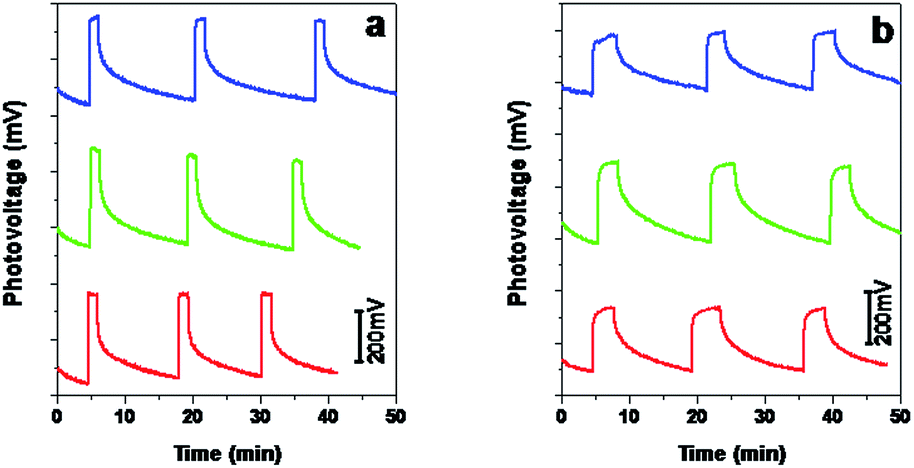 | ||
| Fig. 3 Surface photovoltage transient spectra of the CdSe/ZnO/ITO junction at different wavelengths. (a) Excitation at 350 nm, which corresponds to the ZnO band gap; (b) excitation at 462 nm, 536 nm, and 610 nm, which correspond to 2.0 nm (blue), 2.8 nm (green), and 4.9 nm (red) CdSe nanocrystals, respectively. | ||
 | ||
| Fig. 4 Comparison of surface photovoltage transient spectra of 2.8 nm CdSe nanocrystals in (a) the CdSe/ZnO/ITO junction and (b) the CdSe/ITO junction. Excitation was at 536 nm, which corresponds to the CdSe band gap. | ||
4. Conclusions
In summary, three different sizes of highly monodisperse zinc blende CdSe nanocrystals were chosen to construct heterojunctions with and without ZnO particles. Surface photovoltage (SPV) and surface photovoltage spectroscopy (SPS) were employed to study the photo-induced charge transfer/separation behaviors at these heterojunctions. For CdSe/ITO junctions, all the SPV responses observed involved a higher energy band than the corresponding band-gap excitation of CdSe. The smaller the size of the CdSe crystals, the more blue shifted the SPV. Therefore, it has been clearly shown that the SPV is size-dependent. For CdSe/ZnO/ITO junctions, photovoltage responses were increased greatly, especially in the range above the band gap of the related CdSe nanocrystals. The photovoltage was increased up to 10 times compared to the SPV of bare CdSe. This suggests that efficient charge transfer may occur and that a good alignment of energy levels between CdSe and ZnO is formed. Studies of the SPV transient spectra of the CdSe/ITO and CdSe/ZnO/ITO junctions excited at different wavelengths indicated that different SPV response rates were observed. Generally, a fast decay rate was observed for excitations above the band gap of ZnO. These findings may provide useful guidance on how to choose suitable nanocrystal thin films and adjust related heterojunctions in QLED and solar cell applications, such as monitoring charge transfer efficiency and optimizing the alignment of energy levels by using the SPS technique.Acknowledgements
This work was financially supported by the research project of the National High Technology Research and Development Program of China (863 Program) (no. 2013AA032204), National Natural Science Foundation of China (61474037), and Program for Changjiang Scholars and Innovative Research Team in University (no. PCS IRT1126).Notes and references
- B. S. Mashford, M. Stevenson, Z. Popovic, C. Hamilton, Z. Zhou, C. Breen, J. Steckel, V. Bulovic, M. Bawendi, S. Coe-Sullivan and P. T. Kazlas, Nat. Photonics, 2013, 7, 407–412 CrossRef CAS.
- M. G. Panthani, J. M. Kurley, R. W. Crisp, T. C. Dietz, T. Ezzyat, J. M. Luther and D. V. Talapin, Nano Lett., 2014, 14, 670–675 CrossRef CAS PubMed.
- M. R. Kim and D. L. Ma, J. Phys. Chem. Lett., 2015, 6, 85–99 CrossRef CAS.
- V. L. Colvin, M. C. Schlamp and A. P. Alivisatos, Nature, 1994, 370, 354–357 CrossRef CAS.
- I. L. Medintz, H. T. Uyeda, E. R. Goldman and H. Mattoussi, Nat. Mater., 2005, 4, 435–446 CrossRef CAS PubMed.
- Q. J. Sun, Y. A. Wang, L. S. Li, D. Y. Wang, T. Zhu, J. Xu, C. H. Yang and Y. F. Li, Nat. Photonics, 2007, 1, 717–722 CrossRef CAS.
- L. Qian, Y. Zheng, J. Xue and P. H. Holloway, Nat. Photonics, 2011, 5, 543–548 CrossRef CAS.
- L. Qian, J. H. Yang, R. J. Zhou, A. W. Tang, Y. Zheng, T. K. Tseng, D. Bera, J. G. Xue and P. H. Holloway, J. Mater. Chem., 2011, 21, 3814–3817 RSC.
- H. B. Shen, Q. L. Lin, H. Z. Wang, L. Qian, Y. X. Yang, A. Titov, J. Hyvonen, Y. Zheng and L. S. Li, ACS Appl. Mater. Interfaces, 2013, 5, 12011–12016 CAS.
- H. B. Shen, X. W. Bai, A. Q. Wang, H. Z. Wang, L. Qian, Y. X. Yang, A. Titov, J. Hyvonen, Y. Zheng and L. S. Li, Adv. Funct. Mater., 2014, 24, 2367–2373 CrossRef CAS PubMed.
- L. Kronik and Y. Shapira, Surf. Sci. Rep., 1999, 37, 1–206 CrossRef CAS.
- L. S. Li, Q. X. Jia and A. D. Q. Li, Chem. Mater., 2002, 14, 1159–1165 CrossRef CAS.
- A. D. Q. Li and L. S. Li, J. Phys. Chem. B, 2004, 108, 12842–12850 CrossRef CAS.
- D. Gross, I. Mora-Seró, T. Dittrich, A. Belaidi, C. Mauser, A. Houtepen and E. D. Coco, J. Am. Chem. Soc., 2010, 132, 5981–5983 CrossRef CAS PubMed.
- L. Barnea-Nehoshtan, S. Kirmayer, E. Edri, G. Hodes and D. Cahen, J. Phys. Chem. Lett., 2014, 5, 2408–2413 CrossRef CAS.
- H. B. Shen, H. Z. Wang, Z. J. Tang, J. Z. Niu, S. Y. Lou, Z. L. Du and L. S. Li, CrystEngComm, 2009, 11, 1733–1738 RSC.
- G. Chris, W. Van de and J. Neugebauer, Nature, 2003, 423, 626–628 CrossRef PubMed.
- D. J. Norris and M. G. Bawendi, Phys. Rev. B: Condens. Matter Mater. Phys., 1996, 53, 16338–16346 CrossRef CAS.
- I. Robel, M. Kuno and V. P. Kamat, J. Am. Chem. Soc., 2007, 129, 4136–4137 CrossRef CAS PubMed.
- K. Tvrdy, P. A. Frantsuzov and P. V. Kamat, Proc. Natl.Acad. Sci. U. S. A., 2011, 108, 29–34 CrossRef CAS PubMed.
- B. T. Spann, S. V. Bhat, Q. Nian, K. M. Rickey, G. J. Cheng, X. Ruan and X. Xu, Phys. Chem. Chem. Phys., 2014, 16, 10669–10678 RSC.
Footnote |
| † Electronic supplementary information (ESI) available. See DOI: 10.1039/c5ra02007g |
| This journal is © The Royal Society of Chemistry 2015 |