
Morphological optimization of large-area arrays of TiO2 nanowires & nanotubes for enhanced cold field emission: experiment and theory†
Mingi Choi‡
a,
Zhuo Zhang‡a,
Jingkun Chenb,
Zexiang Dengb and
Kijung Yong*a
aDepartment of Chemical Engineering, POSTECH, Pohang 790-784, Korea. E-mail: kyong@postech.ac.kr
bState Key Laboratory of Optoelectronic Materials and Technologies, School of Physics and Engineering, Sun Yat-Sen University, Guangzhou 510275, People's Republic of China
First published on 11th February 2015
Abstract
Designed by finite elemental modelling, large-area arrays of TiO2 nanowires and nanotubes with differentiated heights mixed together are synthesized on a planar Ti wafer via hydrothermal methods. Experimental measurements reveal that the TiO2 nanowire/tubes arrays with differentiated heights demonstrate a lower shielding effect and their cold field emission (CFE) performances can be further enhanced by increasing their height/diameter ratios for both the nanowires and nanotubes. Theoretically, the TiO2 nanowires and nanotubes are simplified to a “Zero Thickness Charge Disc (ZTCD)” model, based on which their characteristic macroscopic field enhancement factors (γC) are quantified. The theoretically calculated γC values are in good agreement with the experimental ones of the TiO2 nanowires and tubes with a series of geometrical parameters. The TiO2 nanowires and nanotubes have promising potential in CFE. The “ZTCD” model is valuable for future research on quasi-one-dimensional field emitters.
Introduction
Cold Field Emission (CFE), along with its standard theory of Fowler–Nordheim (FN) tunneling,1 has made great achievements and applications in vacuum microelectronics via both experimental investigations and theoretical analyses.2 With rapid development of one-dimensional (1-D) nanotechnologies in recent years, 1-D nano-emitters have demonstrated higher emission efficiency than macroscopic emitters, and the CFE abilities of the 1-D nano-emitters can be enhanced by choosing outstanding emitter materials, increasing the length-diameter ratio or sharpening the top-tip of the emitters. Thus, huge amounts of 1-D nano-emitters made from various materials (such as carbon,3 metals,4 semiconductors5 and even polymers6) and with many kinds of morphologies (such as nano-wires,7 tubes,8 needles9 and etc.) have been explored. From the material view point, titanium oxide (TiO2) is very suitable for CFE owing to its thermal stability and oxide resistibility.10 To date, various arrays of TiO2 nanowires11 and nanotubes12 were prepared as the field emitters. However the CFE of these closely arranged TiO2 nanowires could be weakened greatly due to the shielding effect.13 Although, large arrays of ordered TiO2 nanopillars and nanotubes with suitable and equal interspace could be fabricated by the “atomic layer deposition array defined by etch-back” technique,14 however, high cost of preparation has limited its large-scale production. Thus, developing a simple and economical method for the preparation of the TiO2 nano-emitters to get lower shielding effect and enhancing their CFE abilities is still a challenge. Here, designed by finite element modelling, large-area arrays of TiO2 nanowires with uniform distribution of taller and shorter nanowires were achieved via hydrothermal method for getting lower shielding effect and higher CFE performance.Besides, to study CFE performance of the TiO2 1-D nanostructures in a systematic way, it is essential to combine the experiments with the theoretical studies. So far, based on the FN theory, many theoretical models have been established to study the CFE of 1-D nano-emitters. However, most of them are made from carbon nanotubes (such as floating spheres15 and cylinders16) and metallic nanostructures (such as pyramids,17 hemi-ellipsoidal18 and jellium model19). Little has been reported on the semiconducting emitters due to the complication mainly induced by the electric field penetration into the emitters20 and the surface states.21 For the metallic or semiconducting emitters, the emission ability is quantified by the field enhancement factor (mostly marked as β), which is the ratio of the barrier field near the top-tip of the emitter over the applied macro-field,22 and could be derived via numerical calculations (e.g., solving Laplace equation).23 However, numerical calculations involve complex formula derivation and require special software packages or computational programs. Besides, the FN theory which most models based on is too simple to reflect the effect of the barrier shape on the CFE due to its elementary triangular barrier and Sommerfeld's model.24 To overcome this, we reported the “Charge Disc” model recently to calculate the characteristic macroscopic field enhancement factor [marked as γC, which is the ratio of the characteristic barrier field (FC) over the macroscopic field (FM)]of the ZnO nanotaper based on the Schottky–Nordheim (S–N) barrier via only calculus.25 Although the “Charge Disc” Model is well confirmed by ZnO nanotapers and several other 1-D nano-emitters, the thickness of the disc is not clearly defined, which is very important to the values of the surface charge density of the 1-D nano-emitters. Besides, the “Charge Disc” model has to face the challenge that the heights of the nano-emitters are not uniform. So here we demonstrated the “Zero Thickness Charge Disc (ZTCD)” for the evaluation of the γC values and checked its applicability on the nanowires with differentiated heights mixed together.
As a model system, we have prepared the large-area arrays of vertically aligned TiO2 nanowires and nanotubes via hydrothermal method. The prepared samples exhibited lower shielding effects and enhanced CFE performances with controlled density and aspect ratios of effective emitters. The characteristic macroscopic field enhancement factors were determined from emission current results, which are in good agreement with values obtained from our “ZTCD” model.
Experimental
Materials
Titanium foil (Ti foil, thickness 0.25 mm, 99.7% trace metals basis), sodium hydroxide (NaOH, pellets, semiconductor grade, 99.99% trace metals basis), and hydrochloric acid (HCl, ACS reagent, 37%) were purchased from Sigma Aldrich.Fabrication of TiO2 nanowires and nanotubes
TiO2 nanowires and nanotubes were synthesized by the reported hydrothermal method.26 The cleaned Ti foil which was used for substrate and Ti source was placed in a Teflon-lined stainless steel autoclave filled with NaOH aqueous solution. The morphologies of TiO2 depended on the concentration of NaOH, the nanowire structures and the nanotube structures were obtained with 0.5 M and 0.25 M of the NaOH solution. The autoclave reactor was heated in an electrical oven at 220 °C. Different length of the TiO2 nanowires and nanotubes were fabricated with different reaction time. After the reaction, the reactor was cooled down at RT for 2 h. Sodium titanate arrays were fabricated after this reaction. Then, the foil was immersed in 1 M HCl solution for 10 min to replace the Na+ with H+ to render H2Ti3O7. Then, the foil with titanate nanoarrays was rinsed with water and ethanol and dried for 20 min before being placed in a muffle furnace for heat treatment at 500 °C for 3 h at a ramping rate of 2 °C min−1. After heat treatment, the H2Ti3O7 was converted into TiO2 anatase.27Characterization
The morphologies of nanowires and nanotubes were confirmed by a field-emission scanning electron microscope (FE-SEM, XL30S, Philips) operated at 5.0 kV beam energy and high-resolution scanning transmission electron microscope (HR-STEM; JEM-2200FS with Image Cs-corrector; JEOL) operated at 200 kV beam energy. The crystalline structures were observed by selected-area electron diffraction (SAED) patterns of TEM and X-ray diffractometer (XRD, D/MAX-2500, Rigaku) with Cu Kα radiation (40 kV, 100 mA) results. The XRD spectra were measured in the range of 20–80° with a scan rate of 4° min−1. To prepare the samples for TEM, TiO2 nanoarrays were exfoliated from titanium foil and dispersed in ethanol using an ultrasonicator. The dispersed samples were deposited on a copper grid and were placed in an electrical oven 1 day to remove the ethanol.Field emission
Field emission properties of TiO2 nanostructures were measured in the vacuum chamber at below 5 × 10⁶ torr. The TiO2 nanostructures on the ITO were used as a cathode, and the tungsten was used as an anode, and the two sheet of glass were used as spacers which make the gap of cathode and anode 600 μm. Several times of voltage sweeps from 0 V to 7000 V were conducted to get stabilized current density. After stabilizing, the field emission current could be obtained by voltage sweeps with a high voltage DC power. (HV Rack, Ultravolt).Simulation
The finite elemental modeling was built and calculated by using COMSOL multi-physics.Results and discussion
Morphologies and crystal structure of the TiO2 nanowires and nanotubes
Firstly, in order to design large-area arrays of 1-D TiO2 nano-emitters having lower shielding effect and prepare them in a lower-cost way, we constructed the vertically aligned and closely arranged TiO2 nanowires having spherical top-tips with cylindrical bodies and standing on the substrate with the same diameters and different heights, and then calculated their CFE performance by finite elemental modelling (Fig. 1a). When arrays of the TiO2 nanowires are applied by FM = 20 V μm−1 (upper row of Fig. 1a), the tallest nanowire can exhibit strongest FC = 2.54 × 10³ V μm−1, the FC of the second-tallest one reduces by half and the FC of the shortest ones could be negligible by contrast (bottom row of Fig. 1a). It confirms that the CFE performance of the TiO2 nanowire arrays with the same diameters is much affected by the height and the separate distance of the taller nanowires, and the contribution from shorter nanowires is very little. Thus, the inter-distance of the taller nanowires is important in eliminating the shielding effect efficiently. | ||
| Fig. 1 (a) Potential (upper row) and characteristic barrier field (bottom row) distributions of the vertically aligned TiO2 nanowire arrays having the same diameter and different heights under an applied field about 20 V μm−1. The inset of the upper row shows the modelling net for the top-tip of the nanowire, and the bottom row insets show the enlarged views of field distribution near the top-tips of the tallest, taller and the shortest nanowires, respectively; (b and c) side-view SEM images of 16 h-grown nanowires (b) and 24 h-grown nanotubes (c); (d and e) TEM images of 16 h-grown nanowires (d) and 24 h-grown nanotubes (e). The left insets are their HRTEM images and the right inset of (e) is the enlarged view of the nanotube; (f and g) SAED patterns of 16 h-grown nanowires (f) and 24 h-grown nanotubes (g); (h) XRD patterns of TiO2 nanowires and nanotubes. | ||
Based on the modeling design, the TiO2 nanowire and nanotube arrays with different heights were synthesized via hydrothermal method respectively.
Side-view scanning electron microscope (SEM) observations show large-area arrays of aligned TiO2 nanowires (Fig. 1b) and nanotubes (Fig. 1c) deposited on the Ti substrate. It can be seen that both the nanowires and nanotubes have differentiated heights obviously: the taller ones are protruded among the uniformly grown shorter ones. The transmission electron microscope (TEM) results (Fig. 1d and e) reveal that the width of wires and tubes is 100 and 150 nm respectively, and the tubes, which have hollow inner structure (right inset of Fig. 1e) and tapered in tip part. The atomic structures of wires and tubes were investigated using high resolution TEM (HRTEM, left insets of Fig. 1d and e) and the selected-area electron diffraction (SAED) patterns (Fig. 1f and g). The distance between atomic planes was measured from the HRTEM images viewed along the [010] direction. The distance of (101) atomic planes (0.35144 nm), which can be known from SAED, was measured to be 0.3524 nm from the nanowire samples. In case of nanotubes, the distance between (004) atomic planes (0.23742 nm) was measured to be 0.2387 nm. The SAED patterns of the both samples correspond to the patterns of anatase recorded along the [010] zone axis.
The crystal structures of nanowires and nanotubes were further confirmed by the X-ray diffraction (XRD) patterns (Fig. 1h). We observed most of the peaks of anatase (JCPDS no.86-1157) (101), (004), (200), (211) were found at 2θ = 25.3°, 37.8°, 48.1° and 55.1°, respectively which is well agreed with the SAED pattern. The samples were fabricated on the titanium foil which causes the peaks of the titanium (JCPDS no.44-1294) (100), (002) at 2θ = 35.1° and 38.4°, respectively.
Determination of the γC-array values via “ZTCD” model
Based on “Charge Disc” model, the characteristic macroscopic field enhancement factors (γC-array) were evaluated for the TiO2 nanowire and nanotube arrays, respectively. Before the calculation of γC-array, the TiO2 material should be treated as metal for simplification. It is known that electrons are mainly emitted from the top-surface of the emitter, and the more surface charges collected on the top-surface, the more larger emission current is generated.28 In order to investigate the charge distributions on the surface of the wire- & tube-shaped emitter, the nanowire and the nanotube are approximated as the structures shown in Fig. 2a that a sphere and a ring tangent to the side-face, respectively. By solving the Laplace equation with the aid of finite element analysis under the zero charge boundary condition, we find that the surface charge is mainly concentrated on the upper surface of the sphere for nanowire and the ring for nanotube with their charge densities decreasing rapidly from the top-tip to the bottom under FM = 20 V μm−1. Thus, considering the radius of our prepared TiO2 nanowire diminishes from bottom to top, the nanowire can be simplified as a “Charge Disc” merely consisting of a layer of charges rather than TiO2 (the purple part in the upper row of Fig. 2b), and the nanotube is simplified as a “Charge Ring” (the purple part in the bottom row of Fig. 2b), where r0 and R0 is the top- and bottom-radius of the nanowire, R is the radius of the “Charge Disc”, Rin and Rout are the inner- and outer-radius of the nanotube, and h is the height. In order to deduce the γC-array value of the metallic nanowires and nanotubes, here we take the “Charge Disc” as the example and define its thickness as zero, which we call it “Zero Thickness Charge Disc” and simplified as “ZTCD”. Because we have demonstrated the effect of the charge density σ0 of the “ZTCD” is equal to the surface charge density at the nanowire top-tip, and considering that the top-tip is smaller than the bottom for our prepared TiO2 nanowires, therefore, the radius R of the “ZTCD” can be tangent to the bottom of the sphere and determined by r0, R0 and h of the nanowire as follows:
 | (1) |
 | ||
| Fig. 2 (a) Distributions of the surface charge densities on the metallic nanowire (left) and nanotube (right); (b) geometrical characteristics of the “Charge Disc” for the nanowire (upper row) and “Charge Ring” for the nanotube (bottom row); (c) the constructed “ZTCD” (above the cathode) and image “ZTCD” (below the cathode) model on the opposite side of the cathode;25 (d) three-dimensional (3D) surface for the relationship among R0, h and γC-array of the nanowire arrays, for clarity the insets are the views from other angles; (e) 3D surface for the relationship among Ninterval, PCT and γC-array of the nanowire arrays. | ||
Due to the image force and for the satisfaction of the boundary condition that the “ZTCD” and cathode are equi-potential bodies,29 an equal image “ZTCD” is put on the opposite side of the cathode (Fig. 2c). The potential of the “ZTCD” is zero as the cathode is connected to the ground. By using the accumulation and differential of potentials produced by disc charges, image disc charges and the applied field, the γC-array of the 1-D metallic nanowires can be listed as
| γC-array = (h/R)[1 − exp(−1.1586d/h)] | (2) |
For the nanotubes, considering that the CFE ability can only associate with the area of the “ZTCD” in a given surface charge density and emitter height, so if the area of the Disc and Ring are equal, that is R = (Rout2 − Rin2)1/2, thus the “Charge Ring” can be changed to “ZTCD”. According to eqn (2), if all the nanowires (or nanotubes) have the same radius and height, and stand very closely with each other, such as the interval is only 50 nm, it can be seen from Fig. 2d that the γC-array is slowly increased with h (red curve), and rapidly weakened with the increasing top-radius r0 (white curve) due to the powerful shielding effect.
By contrast, if the heights of the nanowires (or nanotubes) are differentiated, Fig. 2e shows that the γC-array increases rapidly and then slowly with the increasing Ninterval (white curve) and PCT (red curve). Where Ninterval is the number of the shorter nanowires and expresses the inter-distance between the taller nanowires; hT and hS are the average heights of the taller and shorter nanowires, respectively; the percentage PCT = (hT − hS)/hS × 100% describes the height difference between hT and hS. Fig. 2e demonstrates that: (1) the shielding effect decreases from the maximum to disappear with the increasing Ninterval; (2) although γC-array increases with PCT, the shielding effect can also increases with the height/diameter ratio. Thus, there is no need to prepare the taller nanowires much higher than the shorter ones due to the increased shielding effect and therefore the height of our prepared taller TiO2 nanowires are no more than threefold of the shorter ones.
Then, in order to get γC-array value of the TiO2 nanowires and nanotubes, it is necessary to know the intrinsic characteristics of TiO2 under the applied electric field. The “ZTCD” model is based on the improved Fowler–Nordheim (F–N) theory,30 in which the effect of the barrier shape on the FE is taken into account. So, the “technically complete” F–N-type equation containing the barrier shape correction νF is
| JM = αMλCaφ−1(γCFM)2exp(−νFbφ3/2/γCFM) | (3) |
Therefore, only after the φ and νF of the semi-conductive TiO2 is confirmed can we get the theoretical and experimental values of γC-array.
For any semiconducting field emitters, it has been reported that when the applied field penetrates from the surface into the emitter, much more extra electrons will appear on the top surface of the emitter (Fig. 3a). Then, the conduction band has to bend downwards to supply enough holes for accommodating the extra electrons. Therefore, the characteristics of TiO2 under the applied electric field depend on the degree of the band bending, and we have to estimate the magnitude of surface electronic density (σ) caused by the applied field at first, and then calculate the band bending at room temperature. Under the applied external electric field F0, σ and the potential energy Φ satisfy31

 | (4) |
 | ||
| Fig. 3 (a) Schematic of the electrons collected on the top surface of the TiO2 nanowire under applied field; (b) crystal structure of the anatase TiO2 (Excerpted from http://en.wikipedia.org/wiki/Anatase); (c) energy levels of semi-conductive TiO2 and metal under applied field, the red and blue lines represent the bottom of the conduction band and the Fermi level respectively; (d) He 1 (hv = 21.2 eV) UPS curves of the TiO2 nanowires and nanotubes. | ||
Therefore, when the band is bent, the surface charges are almost contributed with the electrons in the conduction band. From eqn (4), the charge density n is proportional to exp[−(Ec − EF)/kbT]. So, when the Fs is neglected and all the extra electrons are filled in the conduction band, the band bending is about 0.098 eV higher than the Fermi Level approximately for TiO2 nanowire and nanotube arrays. And then, when considering the Fs and using self-consistent numeration, the order of magnitude of the σ for Ge is 1012 electron per cm2 under the applied field of 0.3 V Å−1.33 Similarly, the σ of TiO2 has the same order of magnitude and is the difference between the surface electronic density with the band bending and that with no band bending. Because the surface electronic density with the band bending is much higher than that with no band bending, and the electronic density with no band bending is negligible. Thus, if the Fs is taken into account, the band bending is also about 0.098 eV higher than the Fermi Level (Fig. 3c).
Furthermore, if all the extra electrons are filled in not only the conduction band but also the valence band, the bottom of the conduction band also higher than Fermi level about σ = 0.088 eV. The value of 0.088 eV does not make semi-conductive TiO2 exhibit metallic properties. However, TiO2 has much wide band-gap, so most part of the emission still comes from the conduction band and then the influence of valence band on the emission is very little.
Therefore, we should use the affinity χ instead of the work function φ to calculate the γC-array of anatase TiO2 nanostructures. Fig. 3c shows clearly that χ = φ − δ = φ − 0.088 eV, and the work function φ of TiO2 can be deduced from UPS spectra exhibited in Fig. 3d. It can be seen that all of our prepared TiO2 nanostructures have the same lower energy cut-off about 3.326 eV, and higher cut-off of 17.790 eV. By using K. Jacobi' method for deducing the work function of ZnO in 1984,34 φ = hv − ΔE − (EF − EVBM) = [21.2 − (17.790 − 3.326) − 3.2/2] eV = 5.136 eV, where EVBM is the maximum value of the valence band. Thus, the affinity χ = 4.256 eV.
Experimental validation for the theoretical results
To test and verify the “ZTCD” model and eqn (2), experimental validations were performed subsequently. A series of TiO2 nanowire arrays with different growth durations for 4, 8, 12 and 16 hours, and the TiO2 nanotubes for 12 and 24 hours were synthesized, respectively. It can be seen from Fig. 4a–f that the heights of the TiO2 nanowires and nanotubes are increased with the growth durations. With different deposition times of 4, 8, 12 and 16 hours, the heights of taller nanowires are about 3, 9.5, 13 and 19 μm, respectively (upper two curves of Fig. 4g). At the same time, the height/radius ratios (h/R0) are also increased gradually as about 200, 250, 285 and 300, respectively.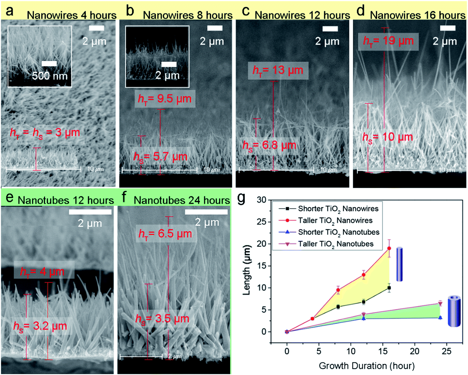 | ||
| Fig. 4 (a–d) Arrays of TiO2 nanowires with the growth time of 4, 8, 12 and 16 hours respectively; (e and f) Arrays of TiO2 nanotubes with the growth time of 12 and 24 hours respectively; (g) The relationship curves between the length and the growth duration of the TiO2 nanowires and nanotubes. | ||
For the TiO2 nanotubes, the heights of taller ones are 4 and 6.5 μm with deposition times for 12 and 24 hours (bottom two curves of Fig. 4g), and the corresponding height/radius ratios are about 15 and 30, respectively.
The experimental JM–FM curves in Fig. 5a exhibit that the turn-on fields of the arrays of TiO2 nanowires with deposition durations of 4, 8, 12 and 16 hours are about 6.7, 6.0, 5.0 and 4.28 V μm−1, respectively. Under an external field of about 9 V μm−1, the current densities of these TiO2 nanowires are about 0.16, 0.52, 3.45 and 3.49 mA cm−2, respectively.
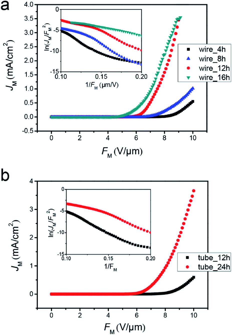 | ||
| Fig. 5 (a and b) JM–FM curves for the arrays of TiO2 nanowires (a) and nanotubes (b) with different growth durations. The insets are their corresponding F–N plots, respectively. | ||
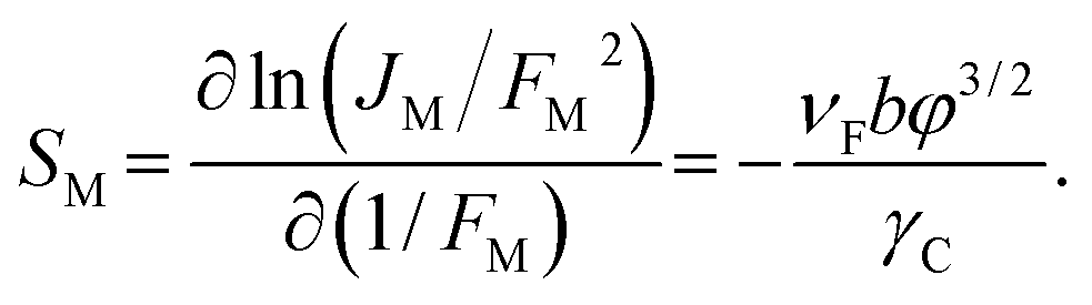
For getting the experimental γC-array of the TiO2 nanowires from their JM–FM curves, it is essential to confirm the shape of CFE barrier and the slop of the F–N plots. Generally, the barrier shape of CFE is simplified as an elementary triangular in FN theory. Then, αM = λC = νF = 1 in eqn (3), and SM = −bχ3/2/γC. So, νF in eqn (3) is not taken into account, which is important for estimating γC or γC-array. Considering that the tip of TiO2 nanowire is modeled as a metallic “ZTCD”, as we discussed above, the Schottky–Nordheim (S–N) barrier is more appropriate for us to estimate the experimental γC-array values. In this case, using the Forbes approximation,35

where K is the relative permittivity of TiO2 and K ≈ 173.36 If χ = 4.256 and SM is taken from the F–N plots shown in the inset of Fig. 5a, the experimental γC-array of the TiO2 nanowires with durations of 4, 8, 12 and 16 hours are estimated to be 551, 732, 1100 and 1471, respectively. Similarly, by using JM–FM curves (Fig. 5b) and corresponding F–N plots (inset of Fig. 5b) of the TiO2 nanotubes with growth durations of 12 and 24 hours, the experimental γC-array of the TiO2 nanotubes are estimated to be 577 and 1156, respectively. The turn-on fields of the nanotubes grown for 12 h and 24 h are 7.5 and 5.8 V μm−1, respectively. Therefore, the CFE performance of the 1-D nano-emitters can be enhanced by increasing their height/radius ratios. Here, the experimental γC-array of the TiO2 nanowires and nanotubes with the heights of 3 and 4 μm have the similar values of 551 and 577, respectively, whereas the top-area of the nanowire is a lot smaller than nanotube. It is due to the shielding effect caused by closely erected nanowires, which have smaller spacing between them and decrease the emission efficiency.

Furthermore, parts of our prepared TiO2 nanowires are bent down or bundled together due to the thinner bodies, which are not efficient for CFE. The SEM images of the TiO2 nanowires before and after the CFE test (Fig. 6) reveal that the nanowires can be straightened and turn more vertical by applying a higher voltage to achieve better CFE abilities of our prepared TiO2 nanowires.
 | ||
| Fig. 6 (a and b) Morphology changes for 12 h TiO2 nanowires before (a) and after (b) CFE test; (c an d) Morphology changes for 16 h TiO2 nanowires before (c) and after (d) CFE test. | ||
Finally, the comparison between the experimental and the theoretical values of γC-array of the TiO2 nanowires and nanotubes are shown in Fig. 7a and b, respectively. It is well known that not all the emitters can have effective emission on the substrate, even the taller ones, so there must be a certain inter-distance between the taller nanowires or nanotubes that have effective emissions. Fig. 7a shows that, for the TiO2 nanowires with different heights of the taller ones (hT) about 3, 9.5, 13 and 19 μm, the experimental values of their γC-array values are in good agreement with the theoretical curves when the inter-distances are about 2.0, 2.1, 3.2 and 4.2 μm, respectively. For the TiO2 nanotubes with the different hT for 4 and 6.5 μm (Fig. 7b), the experimental values agree well with the theoretical curves at the inter-distances about 2.0 and 4.2 μm at the condition that Rin = 4/5Rout, respectively. Here, we notice that it is hard to experimentally estimate the real inter-distance between the taller nanowires or nanotubes that have effective emissions. However, we can mark the top-tips of the taller nanowires and nanotubes and measure the inter-distances between them by using the top-view SEM images. Considering that SEM displays the topography of the surface by scanning the sample and detecting the secondary electrons, some taller nanowires may be missed due to the weakened brightness. Therefore we only used the SEM image for approximately counting the amount of the taller nanowires. The measure results shown in the (ESI†) proved that the experimental inter-distance between the taller nanowires or nanotubes are well-accordance with the theoretical curves. Therefore, the theoretical result from the “ZTCD” model is well confirmed by the experiments. The deviations may result from adsorbed gases, crystal defects and etc.37
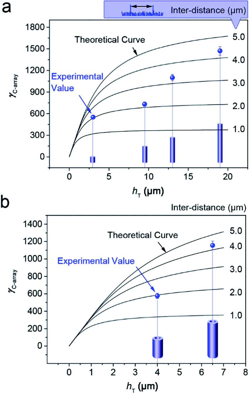 | ||
| Fig. 7 Comparison between the theoretical curves calculated from the “ZTCD” model and the experimental data of γC-array for the TiO2 nanowire (a) and nanotube (b) arrays with different heights of the taller nanowires or nanotubes (hT) and the inter-distances between the taller ones that have effective emissions, respectively. Error bars show the deviation of experimental accuracy. | ||
Conclusions
In summary, arrays of TiO2 nanowires and nanotubes with well differentiated heights and lower shielding effect have been grown on Ti-wafer via hydrothermal method. The CFE performances of the resultant TiO2 nanowires and nanotubes have improved by prolonging the growth durations. The “ZTCD” model has been designed to calculate the γC-array of the TiO2 nanowires and nanotubes. The theoretically calculated γC-array values were well confirmed by the experimental ones. The model can also be used for quasi-1D field emitters of other materials with nano-sized diameters to predict their field emission performance. The enhanced CFE performance of the TiO2 1-D nanostructures presented here promise their practical applications in various electronic devices in the future.Acknowledgements
This work is supported by the National Research Foundation (NRF) of Korea under Grant no. 2013-R1A2A2A05-005344.Notes and references
- R. H. Fowler and L. Nordheim, Proc. R. Soc. London, Ser. A, 1928, 119, 173 CrossRef CAS.
- (a) A. Sandhu, Nat. Nanotechnol., 2007, 2, 133 CrossRef; (b) W. I. Milne, K. B. K. Teo, G. A. J. Amaratunga, P. Legagneux, L. Gangloff, J.-P. Schnell, V. Semet, V. Thien Binh and O. Groening, J. Mater. Chem., 2004, 14, 933 RSC.
- (a) F. S. Baker, J. Williams and A. R. Osborn, Nature, 1972, 239, 96 CrossRef CAS; (b) J. Chen, J. J. Dai, T. Song, M. Y. Ruan, Z. W. Ma, L. Gong, K. Liu, X. H. Zhang, X. J. Hu, J. Zhou and Z. L. Wang, Adv. Funct. Mater., 2011, 21, 2150 CrossRef.
- (a) R. Gomer, J. Chem. Phys., 1953, 21, 293 CrossRef CAS PubMed; (b) E. E. Martin, J. K. Trolan and W. P. Dyke, J. Appl. Phys., 1960, 31, 782 CrossRef PubMed.
- (a) F. S. Baker, Nature, 1970, 225, 539 CrossRef CAS PubMed; (b) X. S. Fang, J. Yan, L. F. Hu, H. Liu and P. S. Lee, Adv. Funct. Mater., 2012, 22, 1613 CrossRef CAS.
- I. Musa, D. A. I. Munindrasdasa, G. A. J. Amaratunga and W. Eccleston, Nature, 1998, 395, 362 CrossRef CAS PubMed.
- (a) A. G. Rinzler, J. H. Hafner, P. Nikolaev, L. Lou, S. G. Kim, D. Tomanek, P. Nordlander, D. T. Colbert and R. E. Smalley, Science, 1995, 269, 1550 CAS; (b) X. D. Wang, J. Zhou, C. S. Lao, J. H. Song, N. S. Xu and Z. L. Wang, Adv. Mater., 2007, 19, 1627 CrossRef CAS; (c) J. C. She, Z. M. Xiao, Y. H. Yang, S. Z. Deng, J. Chen, G. W. Yang and N. S. Xu, ACS Nano, 2008, 2, 2015 CrossRef CAS PubMed.
- (a) W. A. De Heer, A. Châtelain and D. Ugarte, Science, 1995, 270, 1179 CAS; (b) Y. Saito, K. Hamaguchi, S. Uemura, K. Uchida, Y. Tasaka, F. Ikazaki, M. Yumura, A. Kasuya and Y. Nishina, Appl. Phys. A, 1998, 67, 95 CrossRef CAS; (c) J. M. Bonard, J. P. Salvetat, T. Stöckli, W. A. de Heer, L. Forro and A. Chatelain, Appl. Phys. Lett., 1998, 73, 918 CrossRef CAS PubMed.
- (a) S. E. Huq, P. D. Prewett, J. C. She, S. Z. Deng and N. S. Xu, Mater. Sci. Eng. B, 2000, 74, 184 CrossRef; (b) Z. J. Zhang, Y. Zhao and M. M. Zhu, Appl. Phys. Lett., 2006, 88, 033101 CrossRef PubMed; (c) M. Machado, P. Piquini and R. Mota, Nanotech., 2005, 16, 302 CrossRef CAS PubMed.
- J. G. Tao, T. Luttrell and M. Batzill, Nat. Chem., 2011, 3, 296 CrossRef CAS PubMed.
- (a) B. Xiang, Y. Zhang, Z. Wang, X. H. Luo, Y. W. Zhu, H. Z. Zhang and D. P. Yu, J. Phys. D: Appl. Phys., 2005, 38, 1152 CrossRef CAS; (b) J. M. Wu, H. C. Shih and W. T. Wu, Chem. Phys. Lett., 2005, 413, 490 CrossRef CAS PubMed; (c) J. Shen, P. Vincent, Ni. P. Blanchard, J. Nicolle, M. Choueib, S. T. Purcell, P. Poncharal, V. Salles and A. Brioude, J. Vac. Sci. Technol., B: Nanotechnol. Microelectron.: Mater., Process., Meas., Phenom., 2012, 30, 011801 CrossRef.
- (a) M. Miyauchi, H. Tokudome, Y. Toda, T. Kamiya and H. Hosono, Appl. Phys. Lett., 2006, 89, 043114 CrossRef PubMed; (b) X. J. Xu, C. C. Tang, H. B. Zeng, T. Y. Zhai, S. Q. Zhang, H. J. Zhao, Y. Bando and D. Golberg, ACS Appl. Mater. Interfaces, 2011, 3, 1352 CrossRef CAS PubMed.
- L. Nilsson, O. Groening, C. Emmenegger, O. Kuettel, E. Schaller, L. Schlapbach, H. Kind, J. M. Bonard and K. Kern, Appl. Phys. Lett., 2000, 76, 2071 CrossRef CAS PubMed.
- Y. J. Huang, G. Pandraud and P. M. Sarro, Nanotechnology, 2012, 23, 485306 CrossRef PubMed.
- X. Q. Wang, M. Wang, P. M. He, Y. B. Xu and Z. H. Li, J. Appl. Phys., 2004, 96, 6752 CrossRef CAS PubMed.
- C. S. He, W. L. Wang, S. Z. Deng, N. S. Xu and Z. B. Li, J. Phys. Chem. A, 2009, 113, 7048 CrossRef CAS PubMed.
- T. A. de Assis, F. Borondo, C. M. C. de Castilho, F. B. Mota and R. M. Benito, J. Phys. D: Appl. Phys., 2009, 42, 195303 CrossRef.
- E. G. Pogorelov, A. I. Zhbanov and Y. C. Chang, Ultramicroscopy, 2009, 109, 373 CrossRef CAS PubMed.
- Y. Gohda, Y. Nakamura, K. Watanabe and S. Watanabe, Phys. Rev. Lett., 2000, 85, 1750 CrossRef CAS.
- R. Young, J. Ward and F. Scire, Phys. Rev. Lett., 1971, 27, 922 CrossRef CAS.
- R. Stratton, Proc. Phys. Soc., London, Sect. B, 1955, 68, 746 CrossRef.
- H. C. Miller, J. Appl. Phys., 1967, 38, 4501 CrossRef PubMed.
- Y. Alivova and S. Molloi, J. Appl. Phys., 2010, 108, 024303 CrossRef PubMed.
- A. Sommerfeld, Naturwissenschaften, 1927, 16, 825 CrossRef.
- Z. Zhang, G. W. Meng, Q. Wu, Z. Hu, J. K. Chen, Q. L. Xu and F. Zhou, Sci. Rep., 2014, 4, 4676 Search PubMed.
- Y. N. Zhao, U. H. Lee, M. K. Suh and Y. U. Kwon, Bull. Korean Chem. Soc., 2004, 25, 1341 CrossRef CAS.
- M. Choi and K. J. Yong, Nanoscale, 2014, 6, 13900 RSC.
- Z. W. Pan, H. L. Lai, F. C. K. Au, X. F. Duan, W. Y. Zhou, W. S. Shi, N. Wang, C. S. Lee, N. B. Wong, S. T. Lee and S. S. Xie, Adv. Mater., 2000, 12, 1186 CrossRef CAS.
- D. C. Grahame, Chem. Rev., 1947, 41, 441 CrossRef CAS.
- R. G. Forbes, J. Vac. Sci. Technol., B: Nanotechnol. Microelectron.: Mater., Process., Meas., Phenom., 2008, 26, 788 CrossRef CAS.
- A. Modinos, Field, Thermionic and Secondary Electron Emission Spectroscopy, Plenum Press, New York, USA, 1984 Search PubMed.
- F. Cao, G. Oskam, P. C. Searson, J. M. Stipkala, T. A. Heimer, F. Farzad and G. J. Meyer, J. Phys. Chem., 1995, 99, 11974 CrossRef CAS.
- W. B. Shepherd and W. T. Peria, Surf. Sci., 1973, 38, 461 CrossRef CAS.
- K. Jacobi, G. Zwicker and A. Gutmann, Surf. Sci., 1984, 141, 109 CrossRef CAS.
- R. G. Forbes and J. H. B. Deane, Proc. R. Soc. London, Ser. A, 2007, 463, 2907 CrossRef.
- R. van de Krol, A. Goossens and J. Schoonman, J. Electrochem. Soc., 1997, 144, 1723 CrossRef CAS PubMed.
- J. W. Gadzuk and E. W. Plummer, Rev. Mod. Phys., 1973, 45, 487 CrossRef CAS.
Footnotes |
| † Electronic supplementary information (ESI) available. See DOI: 10.1039/c5ra01558h |
| ‡ Equally contributed to this work. |
| This journal is © The Royal Society of Chemistry 2015 |