
 Open Access Article
 This Open Access Article is licensed under a Creative Commons Attribution-Non Commercial 3.0 Unported Licence
Humidity assisted annealing technique for transparent conductive silver nanowire networks†
Nelli
Weiß
*a,
Lars
Müller-Meskamp
b,
Franz
Selzer
b,
Ludwig
Bormann
b,
Alexander
Eychmüller
a,
Karl
Leo
b and
Nikolai
Gaponik
*a
aPhysical Chemistry, TU Dresden, Bergstraße 66b, Dresden, D-01062, Germany. E-mail: nelli.weiss@chemie.tu-dresden.de; nikolai.gaponik@chemie.tu-dresden.de
bInstitute for Applied Photophysics, TU Dresden, George-Bähr-Straße 1, Dresden, D-01062, Germany
First published on 6th February 2015
Abstract
The surfactant polyvinylpyrrolidone (PVP) commonly used to synthesize silver nanowires (AgNW) in solution is known to negatively affect the performance of nanowire-based thin film electrodes. An insulating shell of the polymer hinders tight contact between the nanowires themselves and between the nanowires and substrate, resulting in high sheet resistance of the freshly prepared nanowire films. Here, we develop a simple low-temperature method allowing us to reduce the sheet resistance of AgNW networks and simultaneously improving the optical transmittance. The method is based on the capacity of PVP to absorb moisture which results in a strong decrease in the glass transition temperature of the polymer. The latter leads to softening effects, causing a reduced wire contact resistance already at 60 °C for 90 nm thick AgNWs and even at 45 °C for 35 nm thick AgNWs. As a result, the sheet resistances of the thin film electrodes treated by our method are near to the values conventionally obtained after thermal annealing at temperatures between 140–250 °C. Our humidity assisted low temperature approach is especially advantageous for organic electronics and fabricating devices on thermally sensitive transparent flexible foils.
Introduction
Due to the increasing interest in flexible devices, new transparent conductive electrode materials which could replace the brittle and cost-intensive indium tin oxide are under development. Among carbon nanotubes, nanotroughs, graphene and metal grids, and metal nanowires, especially those made of silver (AgNW) are among the materials demonstrating the most promising performances.1–3 Low-cost synthesis, good chemical stability, low-temperature solution processing of electrodes which is compatible with roll-to-roll manufacturing,4,5 render AgNW electrodes particularly attractive for use in optoelectronic devices. Organic solar cells,6–8 OLEDs,9,10 transparent thin-film heaters11,12 and touch screens13 with AgNWs electrodes have already been demonstrated.Long and thin AgNWs used for the preparation of transparent electrodes are processable from solutions, and polyvinylpyrrolidone (PVP) is typically used as stabilizer, necessary to provide the nanowire shape, its stability and dispersibility in water or alcohols.14,15 Hence, after deposition on a substrate, the contacts between individual NWs are deteriorated by the insulating PVP shell inducing a barrier for electron transport.16–18 As a result, an additional step is required to reduce the junction resistance between individual AgNWs and to obtain high conductivity of electrodes. In the case of silver, well-conducting NW arrays were produced by applying mechanical pressure,19–21 by thermal,17,22–26 nanoplasmonic11,27 or Joule28 annealing. Additional improvement approaches include the fabrication of hybrid materials with polymers,13,29 metal30 or oxide31,32 nanoparticles as well as carbon nanotubes33 and graphene sheets.34–37 Most of these strategies are time- and energy-consuming, involve special complex equipment and exotic nanomaterials. Because of its simplicity, thermal annealing at 140–250 °C remains the most favored method for decreasing the sheet resistance of AgNW films.9,23,29,31,38 However, the utilization of thermal annealing is restricted in the case of organic electronics and especially for flexible substrates. Most of the known plastic foils used for the fabrication of flexible devices tend to deform at processing temperatures above 120 °C.39–42
In our work the moisture induced reduction of the glass transition temperature of PVP is proposed as a technique to allow annealing of AgNW electrodes at low temperatures. We show that the exposition of NW network electrodes to water vapor at 60 °C for 90 nm thick AgNWs and even at 45 °C for 35 nm thick AgNWs causes a considerable decrease in their sheet resistance. At the same time, the total optical transmittance of the NW electrodes could be enhanced. Conducting films on glass, PEN and PET substrates were investigated.
Experimental
Experiments were performed on cleaned 2.5 × 2.5 cm2 BK7 glass substrates (Schott, Mainz, Germany), polyethylene terephthalate (PET) foil (Melinex ST504, DuPont Teijin Films) or polyethylene naphthalate (PEN) foil (Teonex Q65F, DuPont Teijin Films) treated by oxygen plasma and cleaned with the contact cleaner “Nanocleen” (Teknek Ltd, Renfreshwire, UK). Silver nanowires SLV-NW-90 (mean diameter 90 nm, mean length 25 µm) and SLV-NW-35 (mean diameter 35 nm, mean length 10 µm) were purchased from BlueNano, USA. These samples are referred in the following as NW-90 and NW-35, respectively. The as received dispersions were diluted with ethanol to a concentration of 0.2 mg ml−1, sonicated for 15 min and then spray-coated with a nozzle (Fisnar, Wayne (NJ), USA) onto a heated substrate at 80 °C. The spraying distance, moving speed and spraying pressure of the nozzle were 12 cm, 1.5 cm s−1 and 200 mbar, respectively.Following the spray deposition, the electrodes were exposed in a climate cabinet (Thermo Tec) at temperatures between 45 °C and 85 °C to a relative humidity (RH) of between 15% and 85% for 24 h or 3 days for long-term experiments. During these experiments the samples were taken out of the climate cabinet several times for electrical and optical characterization for about 15 minutes a time. To exclude effects of residual water on the conductivity, an additional annealing step (10 min at 105 °C on a hot plate) was applied after removing the samples from the climate cabinet and before measuring the sheet resistance of the electrodes. Because a significant difference of the sheet resistance values before and after the additional drying was not observed, all later experiments were performed without additional annealing. Reference electrodes were fabricated by annealing as sprayed electrodes 30 minutes at 210 °C on a hot plate under ambient laboratory conditions: 23 °C and 48% humidity.
Transmittance and reflectance measurements were performed using a UV-VIS spectrometer with an integrating sphere (Shimadzu). The data reported in this work include transmittance and reflectance of the corresponding glass or plastic substrate. Direct transmittance was acquired by placing the samples perpendicular to the incident light in the spectrometer. Total transmittance was acquired using the integrating sphere setup. To measure the reflectance spectra an integrating sphere and an illumination angle of 5 degree were used. All optical transmission and reflection values are quoted at λ = 550 nm. A four point probe setup (Lucas Labs) was used for measuring the sheet resistance. Scanning electron microscopy (SEM) images were taken with a Carl Zeiss DSM 982 Gemini electron microscope.
Results and discussion
In this work two different AgNW diameters were chosen as representative examples of widely used materials in the field. Transparent conductive electrodes based on NW-90 or NW-35 vary in uniformity, roughness, thermal stability, transparency at a given sheet resistance and haze value. The AgNWs were sprayed onto a glass substrate from ethanol solutions and then kept in the climate cabinet for 24 hours. The temperature was varied in the range from 45 to 85 °C, the relative humidity from 15 to 85%. As these AgNW films were developed for transparent conducting electrode applications, optical spectra and sheet resistances were measured at different time intervals. A typical alteration of optical transmittance spectra of the NW-90 electrode during humidity assisted annealing is shown in Fig. 1a. Unexpectedly, both direct (Tdirect) and total transmittances (Ttotal) increased during this treatment. The main changes happen within the first 30 min of the treatment. Further changes in the optical spectra appeared slowly, depending on the temperature applied and the RH value. The difference between the initial and the final values of the total transmittances is found to especially depend on the NWs density and not on the annealing conditions of the electrode (Fig. S1†). For example, an electrode with an initial Ttotal of 77% showed a Ttotal of 81% after annealing, giving 4% difference from the initial value. An initial Ttotal of 85% could be enhanced only for about 1%. An electrode with an initial Ttotal of 88% became only 0.2% more transparent after annealing.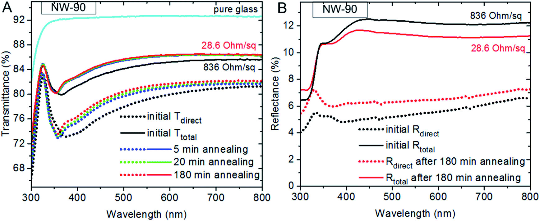 | ||
| Fig. 1 (A) Total transmittance spectra of pure glass substrate (the same before and after annealing) as well as total and direct transmittance spectra of an NW-90 electrode heated at 85 °C/85% RH. (B) Total and direct reflectance spectra of the same NW-90 electrode before and after annealing at 85 °C/85% RH. | ||
An increase of the total transmittance of the electrode can occur due to the changes in scattering behavior of the NW film after annealing. Total and direct reflectance spectra of a NW-90 electrode on glass before and after annealing are shown in Fig. 1b. After annealing, the direct reflectance increased and the total reflectance dropped, indicating a lower scattering of the electrode. The decrease in total reflectance approximately corresponds to the increase in total transmittance. The strong relative increase in direct reflection and less diffuse transmission indicate the film is becoming more planar and less particle-like. This can be well explained by changes in the electrode morphology before and after annealing. Comparing Fig. 2a and b, where NW-90 before and after annealing at 85 °C/85% RH are shown, one can see a softening of the wires, resulting in their slight shape deformation and a closer alignment to each other. Additionally, humidity treated wires have conformal contact to the substrate. Both closer alignment and contact to the substrate are highlighted with white arrows in the higher resolution image shown in Fig. 2c.
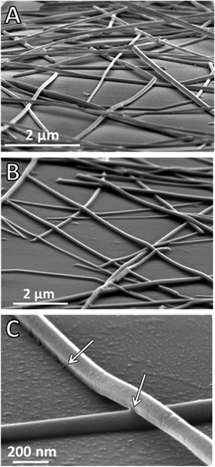 | ||
| Fig. 2 SEM images of Ag90-NW directly after spraying (A), after 180 min annealing at 85 °C/85% RH (B) and 85 °C/70% RH (C) demonstrating changes in the morphology of the NW networks. White arrows in (C) highlight the closer alignment of the wires and a better contact to the substrate. | ||
Alterations in the optical spectra of the NW-35 films at different annealing times are shown in Fig. S2.† Both, changes in the maximum of the transmission spectrum as well as in the value of the transmittance were monitored. Similar to thicker NWs, humidity assisted annealing at RH below 85% leads to relatively compacter films with better contacts between crossing wires, as shown in the corresponding SEM images in Fig. S3.†
Comparing optical data for both types of NWs with their SEM images one may conclude that the observed formation of a denser NW network leads to a lower light scattering and as a result to an increased total transmittance of the electrode.
The changes in film morphologies described above have a direct influence on the electrical properties of NW-90 electrodes. Fig. 3a shows the temporal evolution of their sheet resistance (RS) during annealing at 85 °C and 85% RH. As seen from the figure, the resistance of the electrodes decreased considerably already after the first 30 minutes of the treatment, regardless of the coverage. The highest change of the sheet resistance was observed for samples with the lowest NW density (Fig. 3a). For example, the sheet resistance of the sample with an initial Ttotal of 84% dropped from 836 Ohm sq−1 to 28.6 Ohm sq−1 (ca. 30 times!) after 180 min. For the sample with 75% Ttotal the sheet resistance decreased from 9.5 Ohm sq−1 to 4.3 Ohm sq−1 (ca. 2.2 times only). Taking into account that the junction resistance is the most dominant component in the sheet resistance of the networks with a smaller wire number density closer to the percolation threshold43,44 and becomes less pronounced at high coverages, one can assume that the humid annealing reduces the junction resistance between crossing NWs. For deeper investigation of this phenomenon, solely NW networks with relatively low wire densities, i.e. with initial total transmittances between 81 and 84% for NW-35 networks and between 84 and 87% for NW-90 networks and, thus, expected higher conductivity improvement factors were chosen for further studies.
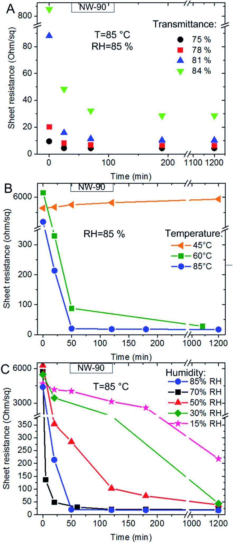 | ||
| Fig. 3 Sheet resistance vs. annealing time for NW-90 films: (A) at different coverages during annealing at 85 °C and 85% RH; (B) at constant RH of 85% and different temperatures; and (C) at constant temperature of 85 °C and different RH values. The blue line representing the sample treated under 85 °C/85% RH is the same in both B and C frames. | ||
The temporal evolution of the sheet resistance of NW-90 electrodes as a function of humidity is displayed in Fig. 3b, c and S4a.† At the highest RH value of 85% a considerable decrease in the sheet resistance of the electrode was detected already at 60 °C (green line in Fig. 3b). If the temperature was kept constant, faster changes were observed at higher RH values (Fig. 3c and S4a†). At 85 °C and RH of 85 or 70% the sheet resistance dropped to the final value within 30 min of annealing. At 50% RH about 2 hours were necessary to achieve the minimum value of the film sheet resistance. At 30% and 15% RH a continuous decrease of film resistivity was detected during 24 hours of measurement. Almost the same dependence of Rs from moisture content was observed for NW-35 networks (Fig. 4 and S4b†). Only at the highest investigated RH value of 85% a considerably different behavior of NW-90 and NW-35 was observed. At 85 °C/85% RH the sheet resistance of the electrode with thinner NWs (blue line in Fig. 4a and b) decreases within the first 120 min of annealing but started to increase gradually thereafter. The reason of this unexpected behavior is the damaged NW network as seen from the SEM image in Fig. S3d.† Obviously, after longer humidity assisted annealing of NW-35 films, the small diameter wires collapse and melt into spherical particles disconnecting the NW network. Moreover, as shown in Fig. S3c,† some spherical particles were already found after annealing of the NW-35 films at 85% RH and 60 °C. But in this case the percolation NW network was not destroyed completely and Rs of the electrode remained low (Fig. 4b, green line).
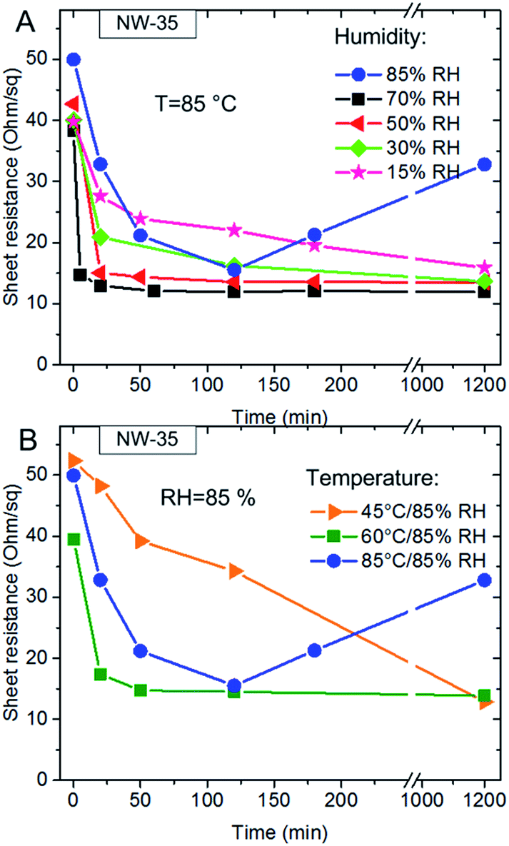 | ||
| Fig. 4 Sheet resistance vs. annealing time for AgNW-35 films: (A) at constant temperature of 85 °C and different RH values; (B) at constant RH of 85% and different temperatures. The blue line represents the sample treated under 85 °C/85% RH similarly in both frames. | ||
The results presented in Fig. 5 compare the performance of NW-90 electrodes obtained after the humidity assisted annealing (85 °C/70% RH) introduced in this work with the same electrodes treated by conventional high temperature annealing on a hot plate at 210 °C, under ambient, i.e. low humidity. For both conditions, nearly the same final values of film sheet resistances were reached demonstrating the potential of our low temperature approach.
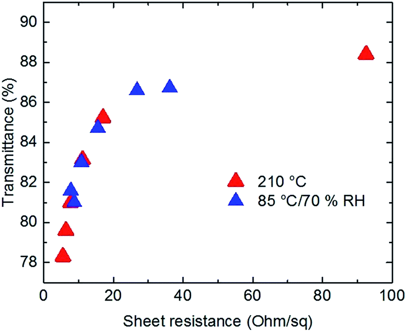 | ||
| Fig. 5 Plot of total transmittance at 550 nm vs. sheet resistance for NW-90 films heated for 90 min at 210 °C on a heating plate (red triangles) and that of films treated for 120 min at 85 °C/70% RH in a climate chamber (blue triangles). | ||
The results discussed above allow us to propose the following mechanism for the observed phenomena. Thermal annealing of the AgNW network is known to be accompanied with the softening and flowing of PVP.17,26 The point at which polymers become rubbery occurs at the glass transition temperature (Tg) and depends on the molecular weight of the polymers as well as on the moisture content. PVP is hygroscopic so that it tends to absorb large amounts of water vapor. The extent of water, which acts as a plasticizer agent, increases continuously with relative humidity, leading to a lowering of the Tg to even below room temperature.45–48 Hence, under humidity assisted annealing in our experiments the PVP shell on the NWs could easyly absorb water, melt and flow away from the NW at as low temperatures as 85 °C, 60 °C and even 45 °C. As a consequence the following effects might be expected:
(i) As was already mentioned above, the originally rigid wires become softer at higher humidity. This effect is well known in hair care cosmetics, where PVP and its copolymers are used as hair sealer.49–51 PVP easily forms films between styled hairs. Nevertheless, these films cannot hold styled hair long in place because of the hygroscopic character of PVP leading to its softening. Therefore, copolymers of PVP containing the less hydrophilic vinyl acetate or N-vinylcaprolactam chains are used in modern moisture resistance hair sprays.49 In our experiments, however, the ability of PVP to adsorb water shows a positive effect on the final electrode properties of both, NW-35 and NW-90 wires. Softening of the wet PVP shell allows elastic alignment of the NWs and thereby improves the electrical contact area between crossing wires.
(ii) Softened by moisture absorption, the rubbery PVP chains of the contacting wires can effectively intercalate52 and interact hydrophobically with each other and the surface. Moreover, softened and melted PVP is flowing down from the top and the side surfaces of the NWs and accumulates below the NWs causing an effective adhesion force, resulting in a tighter contact between crossing NWs and between the NWs and the substrate (marked by white arrows in Fig. 2c). Similar phenomena observed for AgNWs treated by various polymers and surfactants were investigated and described by us in detail in our recent publication.53 This reorganization of PVP on the AgNWs causing a tighter adhesion to the substrate yields a more planar film which is responsible for a reduced scattering cross section and for an increased optical transmission of the electrodes. Such kind of the PVP shell reorganization, e.g. softening, flowing and accumulation below the NWs may also happen under annealing above the glass transition temperature in ambient conditions.
(iii) A partial removal of PVP from the NWs during the annealing might open free paths for surface diffusion of silver atoms and the formation of joints between two contacting wires at a relatively low temperature. Such kind of low temperature sintering was earlier demonstrated for plasma etched AgNWs by Zhu et al.54 Moreover Peng et al. describe a room temperature soldering of copper with AgNW paste after intensive reduction of the organic shell by washing.55 Although we expect soldering effects also in our experiments, this was observed solely for some of the wire joints in NW-35 electrodes (white arrows in Fig. S3b†). If more intensive and prolonged humidity assisted annealing is applied to NW-35 it does not lead to further soldering but to breaking and deformation of the wires into spherical particles due to Raleigh instability27,56 (Fig. S3c and d†). Most likely in these thin wires with relatively higher surface energy morphological changes happen faster than the expected soldering. At the same time, for annealed samples of NW-90 neither deforming nor soldering effects are visible even after 3 days in humidity. The observed decrease of sheet resistance may mainly be attributed to closer contacts formed according to the effects described in (i) above.
The humidity assisted annealing technique presented in this work can be advantageous for fabrication of NW electrodes on thermally sensitive plastic substrates for which annealing over 120 °C is not favourable. For a demonstration the approach was applied to AgNW electrodes spayed onto two types of plastic foil, PET and PEN. As exemplarily shown in Fig. S5a and b,† the total optical transmittance of NW-90 electrodes formed on PEN increased after annealing accompained with a decrease in total reflectance. At the same time the initial sheet resistance of the electrodes was effectively reduced from 406 Ohm sq−1 to 17.8 Ohm sq−1. The same behaviour was observed for PET based electrodes (not shown here). Final sheet resistance values of 17.8 Ohm sq−1 at 81.8% transmittance on PEN and 16.1 Ohm sq−1 at 80.9% transmittance on PET were achieved. It is important to note, that these performances are comparable with literature data for AgNWs on PET and PEN obtained by pressing or annealing under much more sophisticated conditions.11–13,19–21,23,27,43,54,56–67
It should be mentioned that humidity treatment should be applied to NW electrodes for as short time as possible. Recent results68 show that long term (months) of humidity treatment may cause degradation of the AgNWs electrodes.
Conclusions
In summary, we demonstrated a new low temperature technique allowing a fast and efficient reduction of the contact resistance between AgNWs forming transparent conducting electrodes. The technique is based on reducing the glass transition temperature of the PVP stabilizer by increasing the humidity. As a result, softening of PVP, improved alignment and better contact between the AgNWs in the film can be achieved at temperatures as low as 45–85 °C. The performance of humidity assisted annealed electrodes are comparable with typical literature results obtained after conventional high temperature annealing. The great advantage of our simple and straightforward method is its direct applicability to flexible polymer substrates.Acknowledgements
The authors gratefully acknowledge Susanne Goldberg from TU Dresden for the SEM measurements and David Kneppe for spraying the AgNW films. The research leading to these results has received funding from the European Union Seventh Framework Program (FP7/2007-2013) under grant agreement no. 314068.Notes and references
- S. Kumar, B. a. Cola, R. Jackson and S. Graham, J. Electron. Packag., 2011, 133, 020906 CrossRef.
- D. Langley, G. Giusti, C. Mayousse, C. Celle, D. Bellet and J.-P. Simonato, Nanotechnology, 2013, 24, 452001 CrossRef PubMed.
- D. S. Hecht, L. Hu and G. Irvin, Adv. Mater., 2011, 23, 1482–1513 CrossRef CAS PubMed.
- L. Y. L. Wu, W. T. Kerk and C. C. Wong, Thin Solid Films, 2013, 544, 427–432 CrossRef CAS.
- H. H. Khaligh and I. A. Goldthorpe, Nanoscale Res. Lett., 2014, 9, 310 CrossRef PubMed.
- M. Song, D. S. You, K. Lim, S. Park, S. Jung, C. S. Kim, D.-H. Kim, D.-G. Kim, J.-K. Kim, J. Park, Y.-C. Kang, J. Heo, S.-H. Jin, J. H. Park and J.-W. Kang, Adv. Funct. Mater., 2013, 23, 4177–4184 CrossRef CAS.
- W. Gaynor, G. F. Burkhard, M. D. McGehee and P. Peumans, Adv. Mater., 2011, 23, 2905–2910 CrossRef CAS PubMed.
- Z. Yu, L. Li, Q. Zhang, W. Hu and Q. Pei, Adv. Mater., 2011, 23, 4453–4457 CrossRef CAS PubMed.
- W. Gaynor, S. Hofmann, M. G. Christoforo, C. Sachse, S. Mehra, A. Salleo, M. D. McGehee, M. C. Gather, B. Lüssem, L. Müller-Meskamp, P. Peumans and K. Leo, Adv. Mater., 2013, 25, 4006–4013 CrossRef CAS PubMed.
- Z. Yu, Q. Zhang, L. Li, Q. Chen, X. Niu, J. Liu and Q. Pei, Adv. Mater., 2011, 23, 664–668 CrossRef CAS PubMed.
- T. Kim, Y. W. Kim, H. S. Lee, H. Kim, W. S. Yang and K. S. Suh, Adv. Funct. Mater., 2013, 23, 1250–1255 CrossRef CAS.
- C. Celle, C. Mayousse, E. Moreau, H. Basti, A. Carella and J.-P. Simonato, Nano Res., 2012, 5, 427–433 CrossRef CAS.
- J. Lee, P. Lee, H. B. Lee, S. Hong, I. Lee, J. Yeo, S. S. Lee, T.-S. Kim, D. Lee and S. H. Ko, Adv. Funct. Mater., 2013, 23, 4171–4176 CrossRef CAS.
- B. Wiley, Y. Sun and Y. Xia, Langmuir, 2005, 21, 8077–8080 CrossRef CAS PubMed.
- B. Wiley, Y. Sun and Y. Xia, Acc. Chem. Res., 2007, 40, 1067–1076 CrossRef CAS PubMed.
- J.-Y. Kim and N. A. Kotov, Chem. Mater., 2014, 26, 134–152 CrossRef CAS.
- J.-Y. Lee, S. T. Connor, Y. Cui and P. Peumans, Nano Lett., 2008, 8, 689–692 CrossRef CAS PubMed.
- S. Ye, A. R. Rathmell, Z. Chen, I. E. Stewart and B. J. Wiley, Adv. Mater., 2014, 26, 6670–6687 CrossRef CAS PubMed.
- S. De, T. M. Higgins, P. E. Lyons, E. M. Doherty, P. N. Nirmalraj, W. J. Blau, J. J. Boland and J. N. Coleman, ACS Nano, 2009, 3, 1767–1774 CrossRef CAS PubMed.
- S.-E. Park, S. Kim, D.-Y. Lee, E. Kim and J. Hwang, J. Mater. Chem. A, 2013, 1, 14286–14293 CAS.
- Y. Wang, T. Feng, K. Wang, M. Qian, Y. Chen and Z. Sun, J. Nanomater., 2011, 2011, 1–5 Search PubMed.
- T. L. Chen, D. S. Ghosh, V. Mkhitaryan and V. Pruneri, ACS Appl. Mater. Interfaces, 2013, 5, 11756–11761 CAS.
- P. Lee, J. Lee, H. Lee, J. Yeo, S. Hong, K. H. Nam, D. Lee, S. S. Lee and S. H. Ko, Adv. Mater., 2012, 24, 3326–3332 CrossRef CAS PubMed.
- A. R. Madaria, A. Kumar, F. N. Ishikawa and C. Zhou, Nano Res., 2010, 3, 564–573 CrossRef CAS.
- S. Coskun, E. Selen Ates and H. E. Unalan, Nanotechnology, 2013, 24, 125202 CrossRef PubMed.
- C. Sachse, L. Müller-Meskamp, L. Bormann, Y. H. Kim, F. Lehnert, A. Philipp, B. Beyer and K. Leo, Org. Electron., 2013, 14, 143–148 CrossRef CAS.
- E. C. Garnett, W. Cai, J. J. Cha, F. Mahmood, S. T. Connor, M. Greyson Christoforo, Y. Cui, M. D. McGehee and M. L. Brongersma, Nat. Mater., 2012, 11, 241–249 CrossRef CAS PubMed.
- T.-B. Song, Y. Chen, C.-H. Chung, Y. Yang, B. Bob, H.-S. Duan, G. Li, K.-N. Tu and Y. Huang, ACS Nano, 2014, 8, 2804–2811 CrossRef CAS PubMed.
- S. Yun, X. Niu, Z. Yu, W. Hu, P. Brochu and Q. Pei, Adv. Mater., 2012, 24, 1321–1327 CrossRef CAS PubMed.
- H. Varela-Rizo, I. Martín-Gullón and M. Terrones, ACS Nano, 2012, 6, 4565–4572 CrossRef CAS PubMed.
- J. H. Yim, S.-Y. Joe, C. Pang, K. M. Lee, H. Jeong, J.-Y. Park, Y. H. Ahn, J. C. de Mello and S. Lee, ACS Nano, 2014, 8, 2857–2863 CrossRef CAS PubMed.
- F. S. F. Morgenstern, D. Kabra, S. Massip, T. J. K. Brenner, P. E. Lyons, J. N. Coleman and R. H. Friend, Appl. Phys. Lett., 2011, 99, 183307 CrossRef.
- A. J. Stapleton, R. a. Afre, A. V. Ellis, J. G. Shapter, G. G. Andersson, J. S. Quinton and D. a. Lewis, Sci. Technol. Adv. Mater., 2013, 14, 035004 CrossRef.
- M.-S. Lee, K. Lee, S.-Y. Kim, H. Lee, J. Park, K.-H. Choi, H.-K. Kim, D.-G. Kim, D.-Y. Lee, S. Nam and J.-U. Park, Nano Lett., 2013, 13, 2814–2821 CrossRef CAS PubMed.
- I. N. Kholmanov, M. D. Stoller, J. Edgeworth, W. H. Lee, H. Li, J. Lee, C. Barnhart, J. R. Potts, R. Piner, D. Akinwande, J. E. Barrick and R. S. Ruoff, ACS Nano, 2012, 6, 5157–5163 CrossRef CAS PubMed.
- K. Naito, N. Yoshinaga, E. Tsutsumi and Y. Akasaka, Synth. Met., 2013, 175, 42–46 CrossRef CAS.
- B.-T. Liu and H.-L. Kuo, Carbon, 2013, 63, 390–396 CrossRef CAS.
- D.-S. Leem, A. Edwards, M. Faist, J. Nelson, D. D. C. Bradley and J. C. de Mello, Adv. Mater., 2011, 23, 4371–4375 CrossRef CAS PubMed.
- W. A. Macdonald, J. Mater. Chem., 2004, 4–10 RSC.
- H. Zhu, Z. Xiao, D. Liu, Y. Li, N. J. Weadock, Z. Fang, J. Huang and L. Hu, Energy Environ. Sci., 2013, 6, 2105–2111 CAS.
- V. Zardetto, T. M. Brown, A. Reale and A. Di Carlo, J. Polym. Sci. Part B Polym. Phys., 2011, 49, 638–648 CrossRef CAS.
- C.-J. Ni and F. Chau-Nan Hong, RSC Adv., 2014, 4, 40330–40338 RSC.
- C.-H. Chung, T.-B. Song, B. Bob, R. Zhu and Y. Yang, Nano Res., 2012, 5, 805–814 CrossRef CAS.
- S. J. Henley, M. Cann, I. Jurewicz, A. Dalton and D. Milne, Nanoscale, 2014, 6, 946–952 RSC.
- G. Szakonyi and R. Zelkó, Int. J. Pharm. Invest., 2012, 2, 18–25 CrossRef CAS PubMed.
- S. Bhattacharya, D. K. Sharma, S. Saurabh, S. De, A. Sain, A. Nandi and A. Chowdhury, J. Phys. Chem. B, 2013, 117, 7771–7782 CrossRef CAS PubMed.
- J. Teng, S. Bates, D. A. Engers, K. Leach, P. Schields and Y. Yang, J. Pharm. Sci., 2010, 99, 3815–3825 CrossRef CAS PubMed.
- B. C. Hancock and G. Zografi, Pharm. Res., 1994, 11, 471–477 CrossRef CAS.
- C. Wood, Chem. Unserer Zeit, 2002, 2002, 44–52 CrossRef.
- A. Göthlich, S. Koltzenburg and G. Schornick, Chem. unserer Zeit, 2005, 39, 262–273 CrossRef.
- M. J. Root and S. Bohac, J. Soc. Cosmet. Chem., 1966, 17, 595–606 CAS.
- S. Yoshioka and Y. Aso, J. Pharm. Sci., 2007, 96, 960–981 CrossRef CAS PubMed.
- F. Selzer, N. Weiß, L. Bormann, C. Sachse, N. Gaponik, L. Müller-Meskamp, A. Eychmüller and K. Leo, Org. Electron., 2014, 15, 3818–3824 CrossRef CAS.
- S. Zhu, Y. Gao, B. Hu, J. Li, J. Su, Z. Fan and J. Zhou, Nanotechnology, 2013, 24, 335202 CrossRef PubMed.
- P. Peng, A. Hu, H. Huang, A. P. Gerlich, B. Zhao and Y. N. Zhou, J. Mater. Chem., 2012, 22, 12997–13001 RSC.
- S. Karim, M. Toimil-Molares, A. Balogh, W. Ensinger, T. Cornelius, E. Khan and R. Neumann, Nanotech, 2006, 17, 5954–5959 CrossRef CAS.
- J. Jiu, M. Nogi, T. Sugahara, T. Tokuno, T. Araki, N. Komoda, K. Suganuma, H. Uchida and K. Shinozaki, J. Mater. Chem., 2012, 22, 23561–23567 RSC.
- A. R. Madaria, A. Kumar and C. Zhou, Nanotechnology, 2011, 22, 245201 CrossRef PubMed.
- C. Yang, H. Gu, W. Lin, M. M. Yuen, C. P. Wong, M. Xiong and B. Gao, Adv. Mater., 2011, 23, 3052–3056 CrossRef CAS PubMed.
- J. Jiu, T. Sugahara, M. Nogi, T. Araki, K. Suganuma, H. Uchida and K. Shinozaki, Nanoscale, 2013, 5, 11820–11828 RSC.
- C. Mayousse, C. Celle, E. Moreau, J.-F. Mainguet, A. Carella and J.-P. Simonato, Nanotechnology, 2013, 24, 215501 CrossRef PubMed.
- S. S. K. Dong Yun Choi, H. W. Kang and H. J. Sung, Nanoscale, 2013, 5, 977–983 RSC.
- Y. Lee, J.-R. Choi, K. J. Lee, N. E. Stott and D. Kim, Nanotechnology, 2008, 19, 415604 CrossRef PubMed.
- X.-Y. Zeng, Q.-K. Zhang, R.-M. Yu and C.-Z. Lu, Adv. Mater., 2010, 22, 4484–4488 CrossRef CAS PubMed.
- W. Hu, X. Niu, R. Zhao and Q. Pei, Appl. Phys. Lett., 2013, 102, 083303 CrossRef.
- T. Akter and W. S. Kim, ACS Appl. Mater. Interfaces, 2012, 4, 1855–1859 CAS.
- R. M. Mutiso, M. C. Sherrott, A. R. Rathmell, B. J. Wiley and K. I. Winey, ACS Nano, 2013, 7, 7654–7663 CrossRef CAS PubMed.
- C. Mayousse, C. Celle, A. Fraczkiewicz and J.-P. Simonato, Nanoscale, 2015, 7, 2107–2115 RSC.
Footnote |
| † Electronic supplementary information (ESI) available: Changes in total transmittance ΔT vs. initial total transmittance; transmittance spectra of NW-35 electrode vs. annealing time; SEM images of a NW-35 electrode on glass; sheet resistance vs. annealing time at a constant temperature of 60 °C and different RH values; SEM image, transmittance and reflectance spectra of NW-90 electrode on PEN foil. See DOI: 10.1039/c5ra01303h |
| This journal is © The Royal Society of Chemistry 2015 |