Atomic layer-by-layer construction of Pd on nanoporous gold via underpotential deposition and displacement reaction†
Xuejiao Yan‡
a,
Haiyan Xiong‡b,
Qingguo Baia,
Jan Frenzelc,
Conghui Sia,
Xiaoting Chena,
Gunther Eggelerc and
Zhonghua Zhang*a
aKey Laboratory for Liquid-Solid Structural Evolution and Processing of Materials (Ministry of Education), School of Materials Science and Engineering, Shandong University, Jingshi Road 17923, Jinan, 250061, P.R. China. E-mail: zh_zhang@sdu.edu.cn; Fax: +86-531-88396978; Tel: +86-531-88396978
bCenter for Advanced Energy Materials & Technology Research (AEMT), and School of Chemistry and Chemical Engineering, Shandong University, Jinan 250100, China
cInstitut für Werkstoffe, Ruhr Universität Bochum, Bochum 44780, Germany
First published on 10th February 2015
Abstract
Atomic layer-by-layer construction of Pd on nanoporous gold (NPG) has been investigated through the combination of underpotential deposition (UPD) with displacement reaction. It has been found that the UPD of Cu on NPG is sensitive to the applied potential and the deposition time. The optimum deposition potential and time were determined through potential- and time-sensitive stripping experiments. The NPG-Pd electrode shows a different voltammetric behavior in comparison to the bare NPG electrode, and the deposition potential was determined through the integrated charge control for the monolayer UPD of Cu on the NPG-Pd electrode. Five layers of Pd were constructed on NPG through the layer-by-layer deposition. In addition, the microstructure of the NPG-Pdx (x = 1, 2, 3, 4 and 5) films was probed by scanning electron microscopy (SEM), transmission electron microscopy (TEM) and scanning transmission electron microscopy (STEM). The microstructural observation demonstrates that the atomic layers of Pd form on the ligament surface of NPG through epitaxial growth, and have no effect on the nanoporous structure of NPG. In addition, the hydrogen storage properties of the NPG-Pdx electrodes have also been addressed.
1. Introduction
In recent years, ultrathin films of noble metals (Pd or Pt) with only a few atomic layers (AL) coated on other less expensive metals, being used as catalysts, have drawn great attention due to their higher utilization efficiency and better electrocatalytic properties than traditional block catalysts in fuel cells.1,2 A number of methods have been explored to fabricate ultrathin films of Pt on nanostructured materials made of a less expensive or more abundant metal such as Pd3 and Au.4 Chen et al.5 prepared an ultrathin Pd film on a Au surface through physical vapor deposition, and further investigated the mechanism of the promotional effect of Au in a Pd–Au alloy catalyst through acetoxylation of ethylene to vinyl acetate.Palladium nanomaterials, well-known for their remarkable capacity in hydrogen absorption and less expensive than platinum,6 are widely used in catalysis, optical sensors7 and hydrogen sensors.8 In order to maximize their performance in all of these applications, the size and shape of Pd nanomaterials are critical parameters.9 The atomic layer-by-layer construction of Pd plays a crucial role in its applications for different fields. For deposition of nanostructured Pd, the substrate with high chemical stability, oxidation resistance and good biocompatibility need be carefully chosen. Recently, nanostructured Au attracted a great deal of attention in applications such as catalysis, drug delivery, biological labeling, etc.9,10 Among kinds of Au nanostructures, unsupported nanoporous gold (NPG) demonstrates remarkable catalytic activity for CO oxidation at low temperatures11,12 and for direct catalytic oxidation of methanol.13 NPG film made by dealloying of Au/Ag alloys has a unique nanoporous structure with good electrical conductivity,14 and is a good substrate for Pd deposition.
Underpotential deposition (UPD) is electrodeposition of a single monolayer or submonolayer amount of foreign metals and non-metals on the substrate at a potential positive than the thermodynamic potential.6,15,16 Up to date, UPD has been widely used to prepare catalyst monolayers with precise coverage. When the interaction energy between M–S (metal M and metal S) is larger than that between M–M, UPD will take place with M deposition on the S substrate.17 In addition, the structure of the substrate surface plays an important role in the UPD process, and determines specific features of the growing deposition layer. Numerous UPD systems have been extensively investigated on polycrystalline or single crystalline noble metal substrates (Pt and Au), such as Cu2+, Pb2+, Bi3+, Ag+ etc.6,18–30 For example, Shao et al.28 designed the dealloyed PdNi/C core–shell catalysts involving Pt displacement of a UPD Cu monolayer.
Because Cu UPD can occur on both Au and Pd surfaces, this kind of operation can be repeated to form ultrathin Pd films/layers in a precise manner from one to several atomic layers. In this work, we demonstrate how the UPD technique can be applied to fabricate ultrathin Pd film on NPG surface in an atomic layer-by-layer mode through the combination of UPD with displacement reaction. The NPG films were firstly prepared by the dealloying of commercial Ag–Au leaves. Thus the UPD potential of Cu on NPG was determined through time- and potential-sensitive stripping experiments. We have also found that the deposited Pd layer has a visible influence on the subsequent UPD of Cu, and further investigated the hydrogen storage of the Pd coated NPG electrodes.
2. Experimental
In this work, all aqueous solutions were prepared from analytical grade (AG) reagents and ultrapurified water (18.2 MΩ). Before electrochemical measurements, the solutions were purged with high-purity nitrogen for at least 30 min. The UPD steps and replacement steps were performed under a nitrogen atmosphere.NPG films were prepared through dealloying commercial white gold leaves (100 nm thick, 12 carat, Au50Ag50 in wt%, Noris-Blattgold GmbH, Germany) by floating them in a concentrated HNO3 (65 wt%) solution at room temperature for 30 min.17 The as-prepared NPG films were carefully rinsed with ultrapurified water several times. Afterwards, the NPG films were loaded onto the surface of a glass carbon (GC) electrode, and then were dried in vacuum. All electrochemical experiments were performed in a three-electrode cell with a CHI 760E Potentiostat at room temperature. The GC electrode loaded with NPG was used as the working electrode. A Pt plate was served as the counter electrode, and an Ag/AgCl electrode (KCl-saturated) was used as the reference electrode.
The UPD of Cu on NPG was carried out in a 0.5 M H2SO4 solution containing 1 mM CuSO4. Afterwards, the electrode was immediately immersed into a 250 mM HCl solution containing 0.5 mM PdCl2, holding for 10 min for displacement of Cu layer by Pd. Thus a Pd monolayer decorated NPG electrode was obtained and designated as NPG-Pd1. Because UPD of Cu can occur on both Au and Pd surfaces, NPG-Pdx with different atomic Pd layers (namely, NPG-Pd2, NPG-Pd3, NPG-Pd4 and NPG-Pd5 for 2, 3, 4, and 5 Pd layers respectively) can be obtained by changing the deposition potential of corresponding system and repeating the above UPD and displacement steps. The electrochemical behavior of the as-prepared NPG-Pdx electrodes was characterized by means of cyclic voltammetry (CV) in the 0.5 M H2SO4 solution and 0.1 M KOH solution.
Scanning electron microscope (SEM, Quanta FEG 250) was used to characterize the morphology of the NPG-Pdx electrodes. The microstructure of NPG-Pdx was also characterized using transmission electron microscopy (TEM, FEI Tecnai G2) and selected-area electron diffraction (SAED). The scanning transmission electron microscopy (STEM) images were also obtained under high angle annular dark field (HAADF) mode. In addition, the chemical compositions of the as-prepared NPG-Pdx electrodes were determined by energy dispersive X-ray spectroscope (EDX) in the SEM. Nanobeam-EDX (NB-EDX) analysis was also performed on the NPG-Pdx electrodes by the FEI Tecnai G2 microscope under the HAADF mode.
3. Results and discussion
3.1 Voltammetric behavior of NPG
The dealloying of white gold leaves results in the formation of NPG films with an open, bicontinuous ligament-channel structure which could be found in many literatures.12–14 Before dealloying, the Ag–Au film is bright silvery white (left part of Fig. 1a). After dealloying, the as-obtained NPG film is dark brown as shown in right part of Fig. 1a. Fig. 1b shows a typical CV curve of the NPG electrode in the N2 purged 0.5 M H2SO4 solution. The CV curve includes a broad anodic peak at the potential of >1.1 V vs. Ag/AgCl due to the formation of Au–O and a cathodic peak at around 0.93 V vs. Ag/AgCl corresponding to the subsequent reduction of Au–O. And it also exhibits a flat double-layer charging/discharging between 0 and 0.72 V vs. Ag/AgCl as reported in the literature.31,32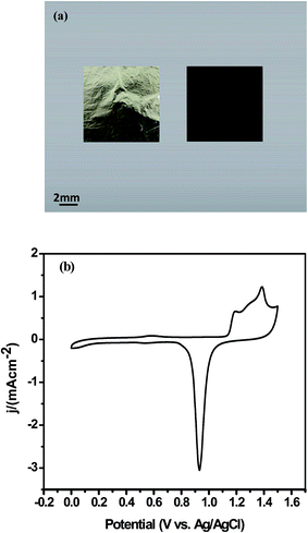 | ||
| Fig. 1 (a) Macrographs of the NPG film before (left) and after (right) dealloying. (b) CV of the NPG electrode in the 0.5 M H2SO4 solution at the scan rate of 50 mV s−1. | ||
3.2 UPD of Cu on NPG electrode
Before deposition of Cu on NPG, the voltammetric behavior of Cu on the NPG electrode was recorded in the 0.5 M H2SO4 + 1 mM CuSO4 solution. The potential was scanned in the range from 0.6 to −0.04 V vs. Ag/AgCl at 2 mV s−1, with the initial potential being 0.6 V vs. Ag/AgCl. Fig. 2 shows the corresponding CV curve of the NPG electrode. The CV features are similar to those reported in the literature.33,34 The negative-going potential sweeping results in a broad peak A at around 0.27 V vs. Ag/AgCl, followed by a small peak B at about 0.026 V vs. Ag/AgCl. The presence of peak A and B originates from the UPD of Cu2+ on the surface of NPG, corresponding to the two steps of Cu UPD. The oxidation peaks (A′ and B′) in the positive scan correspond to the stripping of UPD Cu.17,35 Peak A is the first stage of Cu UPD. The corresponding A′ section includes two sharp peaks which are related to Au (111) and Au (100) surface.36 Here, the left intense part of A′ is the main peak, and the right part of A′ is defined as the shoulder peak for convenience (as highlighted by an arrow in Fig. 2). As can be seen from peak C, sweeping the potential to more negative values leads to a sharp increase in current, which signals the onset of bulk Cu deposition. This results in the deposition of Cu overlayers on the substrate metal. C′ is the corresponding stripping peak of bulk Cu. So it is reasonable to speculate that the end part of peak B is the boundary of UPD and bulk deposition regions.31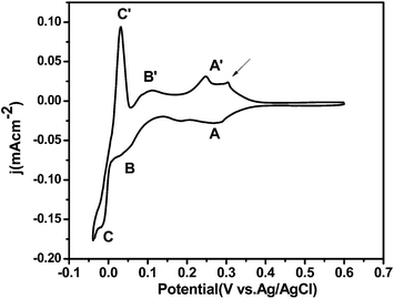 | ||
| Fig. 2 CV of the NPG electrode in the 0.5 M H2SO4 + 1 mM CuSO4 solution at the scan rate of 2 mV s−1. | ||
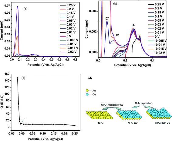
Improper potential will result in deposition of either submonolayer or bulk Cu. In order to achieve maximum Cu monolayer coverage without bulk Cu deposition, two parameters including deposition potential and deposition time should be optimized. For optimizing the UPD potential, the NPG electrode was operated at different potentials in the 0.5 M H2SO4 + 1 mM CuSO4 solution in an amperometric i-t mode, all for a constant period of 240 s. Soon afterwards, the anodic stripping voltammograms were recorded by sweeping the electrode potential from the deposition potential to the final potential of 0.7 V vs. Ag/AgCl, which was high enough to completely remove the deposited Cu. Fig. 3a shows the stripping curves of the NPG electrode with Cu deposited at different potentials. Peak A′/B′ and C′ correspond to the stripping of UPD Cu and bulk-deposited Cu respectively. The stripping peak of Cu evolves quickly with the decrease of the deposition potential, which could be clearly observed from the enlarged plot of Fig. 3a (Fig. 3b). It is clear that the bulk deposition of Cu takes place below −0.01 V vs. Ag/AgCl. The present results are consistent with the report by Khosravi and Amini.37 Then we got the stripping charges of Cu by integrating the area under the stripping voltammogram. Fig. 3c shows the change of stripping charges against the deposition potential. The charge values increase slowly with decreasing deposition potential from 0.25 to 0 V vs. Ag/AgCl. However, the charge values increase sharply when the deposition potential further decreasing to a more negative value. And the charge for the deposition potential of −0.02 V vs. Ag/AgCl is even two orders of magnitude larger than that for the potential above 0 V vs. Ag/AgCl. Moreover, it can be seen that the deposition of Cu is quite sensitive to the change of potential in the UPD region. Thus we can roughly determine the monolayer UPD potential of Cu around −0.005 V vs. Ag/AgCl, as highlighted by an arrow in Fig. 3c. Fig. 3d shows the schematic illustration of Cu deposition on the NPG surface. Initially, Cu atoms deposit on the NPG surface forming a uniform monolayer through the UPD process. When the potential goes more negatively, the bulk deposition of Cu occurs on the electrode surface.
In order to find the more accurate deposition potential and deposition time, we conducted a series of experiments at −0.007 and −0.009 V vs. Ag/AgCl all for 60, 120, 180, 240, 300 and 360 s. Fig. 4 shows the stripping curves of the NPG electrode with the deposited Cu. The intensity of the stripping peaks (B′ and C′) increases obviously as time growing when the applied deposition potential is −0.009 V vs. Ag/AgCl (Fig. 4a). And the stripping peaks increase relatively slow when the deposition time is less than 240 s. Once the deposition time is longer than 240 s (for example, 300 s), the stripping peaks increase sharply, indicating the occurrence of bulk deposition of Cu. This suggests that 240 s is long enough to get monolayer Cu UPD on NPG when the applied potential is negative enough. Longer time will result in bulk Cu deposition. When the deposition potential becomes a little more positive (for instance −0.007 V vs. Ag/AgCl, Fig. 4b), however, the stripping peak intensity increases gradually and peak C′ does not emerge even though the deposition time reaches 360 s. This indicates that −0.007 V vs. Ag/AgCl is too positive to obtain monolayer UPD of Cu on the NPG surface. According to the above results, the optimum deposition potential and time were determined to be −0.009 V vs. Ag/AgCl and 240 s for the monolayer UPD of Cu on NPG, respectively.
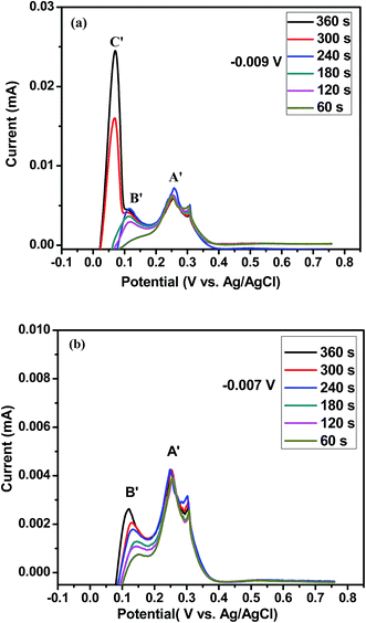 | ||
| Fig. 4 Stripping voltammograms of Cu on NPG deposited at the potential of (a) −0.009 and (b) −0.007 V vs. Ag/AgCl for different times in the 0.5 M H2SO4 + 1 mM CuSO4 solution. | ||
3.3 UPD of Cu on NPG-Pdx
To obtain NPG-Pd, the NPG electrode modified with UPD Cu was immersed into the 0.5 mM PdCl2 and 250 mM HCl solution for 10 min to insure complete displacement reaction. The basic deposition protocol employed here entails replacing a UPD metal adlayer on gold with Pd via a spontaneous replacement process.30 The stoichiometry of the reaction between Pd2+ and Cu is 1![[thin space (1/6-em)]](https://www.rsc.org/images/entities/char_2009.gif) :
:![[thin space (1/6-em)]](https://www.rsc.org/images/entities/char_2009.gif) 1 (Cu + Pd2+ = Pd + Cu2+). Supposing that all of the UPD Cu is oxidized to Cu2+, this replacement can result in the formation of Pd monolayer on the NPG electrode (NPG-Pd1).
1 (Cu + Pd2+ = Pd + Cu2+). Supposing that all of the UPD Cu is oxidized to Cu2+, this replacement can result in the formation of Pd monolayer on the NPG electrode (NPG-Pd1).
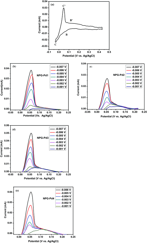
The next thing was to determine the deposition potential of monolayer Cu UPD on the surface of NPG-Pd1. First the voltammetric behavior of Cu on NPG-Pd1 electrode was probed in the 0.5 M H2SO4 + 1 mM CuSO4 solution (Fig. 5a). The CV profile of the NPG-Pd1 electrode is different from that of the NPG electrode, with the absence of peaks A and A′. For the NPG-Pd1 electrode, it is difficult to unambiguously discern the UPD and bulk deposition of Cu from the CV curve. Thus we try to determine the deposition potential for the monolayer UPD of Cu on the NPG-Pd1 electrode through the integrated charge control. That is, when the charge corresponding to the stripping peak (B′ and C′) is equal to that of monolayer Cu UPD on NPG, the applied potential is believed to be the UPD potential for the monolayer Cu on NPG-Pd1.
The NPG-Pd1 electrode was operated at different potentials in the 0.5 M H2SO4 + 1 mM CuSO4 solution in the amperometric i-t mode at a constant period of 240 s. The anodic stripping voltammogram (Fig. 5b) was recorded by sweeping from the deposition potential to 0.22 V vs. Ag/AgCl. Afterwards, the charge could be obtained through integrating the area under the stripping peaks (B′ and C′). The integrated charge (382.3 μC) at the potential of −0.005 V vs. Ag/AgCl is approximately equal to that (386.9 μC) of monolayer Cu UPD on NPG. Thus the optimum deposition potential and deposition time were determined to be −0.005 V vs. Ag/AgCl and 240 s for the monolayer Cu UPD on the NPG-Pd1 electrode. Under this condition we could obtain monolayer Cu coverage on the NPG-Pd1 substrate. Subsequently, the as-prepared NPG-Pd1-Cu electrode was immersed into the Pd2+ solution for galvanic replacement to prepare two-layer Pd decorating NPG electrode (NPG-Pd2). Similarly, we could determine the deposition potential of monolayer Cu on the NPG-Pd2, NPG-Pd3 and NPG-Pd4 electrode (Table 1). The corresponding stripping curves are presented in Fig. 5c–e, and analogous scenarios could be observed for all the stripping curves. Moreover, the deposition potential of the NPG-Pdx electrodes slightly increases with increasing Pd layers (Table 1).
| Substrate | NPG | NPG-Pd1 | NPG-Pd2 | NPG-Pd3 | NPG-Pd4 | NPG-Pd5 |
|---|---|---|---|---|---|---|
| UPD potential (V vs. Ag/AgCl) | −0.009 | −0.005 | −0.005 | −0.003 | −0.003 | |
| Charge for H adsorption/desorption (μC) | 229.9 | 260.1 | 331.0 | 398.0 | 455.1 |
3.4 Characterization of the NPG-Pdx electrodes
Through the combination of Cu UPD with the displacement reaction, the NPG-Pdx electrodes could be constructed with atomic layer-by-layer control. Fig. 6 shows the CVs of the NPG-Pd1 and NPG-Pd2 electrodes in the nitrogen purged 0.1 M KOH solution. For comparison, the CV of the NPG electrode is also included. The CV for the bare NPG electrode displays an oxidation peak initiating at 0.21 V vs. Ag/AgCl in the positive-going potential scan and a reduction peak at 0.1 V vs. Ag/AgCl in the cathodic scan, which is typical for NPG in alkaline solutions.31 In contrast, the presence of Pd causes markedly different electrochemical responses. It is more clearly seen that the reduction peak of gold oxide becomes greatly suppressed, accompanying the appearance of a new strong reduction peak for Pd oxide at −0.14 V vs. Ag/AgCl. This means that most of NPG surface is covered by Pd atoms (near monolayer). Similar CV results of NPG-Pd have also been reported in the literature.31 The coverage of Pd1 layer on the NPG surface was calculated. First the uncovered Au (value: 0.19) was calculated by integrating the reduction peak of Au oxide (using 400 μC cm−2 as the conversion factor37) on the CV curve of NPG-Pd1. Then the coverage of Pd on the NPG surface was determined to be 0.81 (1 − 0.19) for the NPG-Pd1 electrode. For the NPG-Pd2 electrode, the signal of reduction peak of Au oxide almost disappears, indicating the complete coverage of Pd layers on the NPG surface (Fig. 6). Typical CV curves of nanostructured Pd are observed for the other NPG-Pdx electrodes (that is, NPG-Pd3, NPG-Pd4 and NPG-Pd5) in the dilute KOH solution.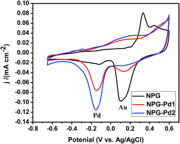 | ||
| Fig. 6 CVs of the NPG, NPG-Pd1 and NPG-Pd2 electrodes in the 0.1 M KOH solution at the scan rate of 50 mV s−1. | ||
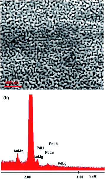
Some NPG-Pdx electrodes were selected for SEM, TEM and STEM characterization. Fig. 7 shows the typical SEM image of the NPG-Pd2 electrode. The electrode displays a typical open, bicontinuous ligament-channel structure, which is quite similar to that of the bare NPG electrode. The corresponding EDX results verify the presence of minor Pd in the NPG-Pd2 electrode, and a typical EDX spectrum is presented as Fig. 7b. According to the CV (Fig. 6) and EDX (Fig. 7b) results, the atomic Pd layers were successfully constructed on the NPG electrode. In addition, we have inspected all the NPG-Pdx electrodes by SEM, and similar nanoporous structures were observed in spite of different Pd layers. As shown in Fig. S1,† the morphology of NPG-Pd5 still maintains the bicontinuous nanoporous structure with smooth surface.
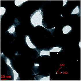
Fig. 8 and S2† show the TEM results of the NPG-Pd2 and NPG-Pd4 electrodes respectively. The three-dimensional nanoporous structure could be clearly observed with the Au surface being covered by a uniform Pd deposit. The average length scale of ligaments/channels is around 30 nm. The related SAED patterns of the NPG-Pd2 (inset of Fig. 8) and NPG-Pd4 (inset of Fig. S2†) confirm the single-crystalline nature of Pd deposited NPG film in the selected area (∼200 nm in diameter). The zone axis of NPG-Pd2 is close to the [001] direction of face centered cubic (fcc) Au (inset of Fig. 8). And the zone axis of NPG-Pd4 is the [110] direction of fcc Au (inset of Fig. S2†). The electron diffraction results demonstrate that at least a significant portion of Pd layers keeps the same crystallographic orientation as the NPG substrate during the displacement process. Additionally, a typical STEM image of NPG-Pd4 is shown in Fig. S3a.† The ligaments also show relatively smooth surfaces. The NB-EDX analysis (Fig. S3b and c†) indicates that both the center and border of the ligament are covered by Pd atoms. On the basis of the above results, it is reasonable to assume that the atomic Pd layers decorate on the ligament surface through the epitaxial growth. In comparison, as reported in the literature,38–40 it is difficult to handle the atomic deposition of Pd on nanostructured gold substrate through regular electrodeposition. During regular electrodeposition, Pd tends to form nanoparticles. For example, Ke et al.40 have reported the different morphology of NPG before and after Pd electrodeposition. After electrodeposition, the NPG framework was packed by the dense and uniform Pd nanoparticles.
In addition, we have done comparison experiments to deposit Pt on NPG using similar UPD and displacement reaction. Even for NPG-Pt1, Pt atoms tend to form an island-like or particle-like structure on the NPG surface (Fig. S4†), which is quite different from the scenario of Pd deposition. Previous reports have shown that the deposition of Pt on Au surface is definitely one monolayer high, but they are partially interconnected nano-clusters.16,41 However, the morphology of Pt after galvanic replacement in our work (Fig. S4 in ESI†) is similar to that reported in the literature.42,43 Their results suggest that Pt nanoparticles grew over the substrate surface. The Pt ions appear to be reduced to Pt atoms which diffuse over the substrate surface due to very high Pt surface energy,43,44 creating very small Pt nanoparticles on the substrate surface. In the case of Pt deposition on NPG, similar morphology of Pt has also been reported in the previous report.17 One possible reason lies in the displacement reaction.42,45 For Pd, the reaction is given as, Cu + Pd2+ = Pd + Cu2+, and the atomic ratio of Pd/Cu is 1![[thin space (1/6-em)]](https://www.rsc.org/images/entities/char_2009.gif) :
:![[thin space (1/6-em)]](https://www.rsc.org/images/entities/char_2009.gif) 1. For Pt, however, the reaction is given as, 2Cu + Pt2+ = Pt + 2Cu+, where the Cu atom is oxidized to Cu+.45 And the atomic ratio of Pt/Cu is 1
1. For Pt, however, the reaction is given as, 2Cu + Pt2+ = Pt + 2Cu+, where the Cu atom is oxidized to Cu+.45 And the atomic ratio of Pt/Cu is 1![[thin space (1/6-em)]](https://www.rsc.org/images/entities/char_2009.gif) :
:![[thin space (1/6-em)]](https://www.rsc.org/images/entities/char_2009.gif) 2. Even if the UPD-Cu is monolayer, the Pt layer is less than one atomic layer after displacement reaction and Pt atoms may form nanoclusters or nanoparticles. Of course, the underlying mechanism for this difference of Pd and Pt deposition should be probed in the following work (for example, theoretical calculation like DFT).
2. Even if the UPD-Cu is monolayer, the Pt layer is less than one atomic layer after displacement reaction and Pt atoms may form nanoclusters or nanoparticles. Of course, the underlying mechanism for this difference of Pd and Pt deposition should be probed in the following work (for example, theoretical calculation like DFT).
3.5 Voltammetric behavior of the NPG-Pdx electrodes
Fig. 9 shows cyclic voltammograms of the NPG and NPG-Pdx electrodes in the 0.5 M H2SO4 solution at a scan rate of 50 mV s−1. For comparison, the CV curve of bulk Pd foil is also included (Fig. S5†). No characteristic peak could be observed for the bare NPG electrode. The voltammetric profile for Pd foil is similar to others previously reported.46 The bulk Pd electrode does not display well-separated processes of hydrogen adsorption/absorption and desorption. It is worth noting that the CV signals for hydrogen absorption and desorption reveal a hysteresis, which demonstrates that the absorption and desorption of hydrogen occur in different potential ranges.47 Comparing to the bulk Pd foil electrode, there exists the separation of hydrogen adsorption and absorption processes for the NPG-Pdx electrodes. The CV profiles of the NPG-Pdx electrodes show two pairs of peaks (A and A′, B and B′), corresponding to the adsorption/absorption of hydrogen in the cathodic scan and the desorption of hydrogen in the anodic scan. Peak A and A′ at the more positive potential is due to the UPD (adsorbed) H-atoms, while peak B and B′ at the more negative potential is related to the bulk (absorbed) H-atoms.46 It is a typical electrochemical behavior of Pd-decorated electrode in terms of hydrogen adsorption/desorption with broad redox waves appearing in the potential region between −0.25 and 0.25 V vs. Ag/AgCl. The separation of surface adsorption from bulk absorption is one of the advantages of Pd nanofilms rather than bulk Pd electrodes.48,49 And it is also the characteristic of nanoporous Pd films and nanoparticles.50,51 Furthermore, the current of the adsorption/desorption peaks gradually increases with increasing Pd layers on the NPG surface. The involved charge for hydrogen adsorption/desorption was calculated for each NPG-Pdx electrode, and the results are listed in Table 1. The charge continuously increases with the increase of Pd layers, suggesting the enhanced hydrogen storage capacity for the electrode with more Pd layers. Therefore, the present NPG-Pdx electrodes can be used as hydrogen sensors and electrocatalysts. And the related applications in sensing and electrocatalysis will be done in the following work.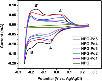 | ||
| Fig. 9 CVs of the NPG and NPG-Pdx electrodes in the 0.5 M H2SO4 solution at the scan rate of 50 mV s−1. | ||
4. Conclusions
In summary, atomic layer Pd could be constructed on NPG through the combination of UPD with displacement reaction. The UPD of Cu on NPG is sensitive to the applied potential and the deposition time. The optimum deposition potential and time are −0.009 V vs. Ag/AgCl and 240 s for the monolayer UPD of Cu on NPG, respectively. The NPG-Pd electrode shows a different voltammetric behavior in comparison to the bare NPG electrode. Moreover, the deposited Pd layer has a visible influence on the subsequent UPD of Cu on the NPG-Pdx electrodes. The atomic layers of Pd form on the ligament surface of NPG through the epitaxial growth, and have no effect on the nanoporous structure of NPG. In addition, the deposition of atomic layer Pd could greatly enhance the hydrogen storage capacity of the NPG electrode, which increases with the increase of Pd layers.Acknowledgements
The authors gratefully acknowledge financial support by National Basic Research Program of China (973, 2012CB932800), National Natural Science Foundation of China (51371106), Program for New Century Excellent Talents in University (MOE, NCET-11-0318), Specialized Research Fund for the Doctoral Program of Higher Education of China (20120131110017) and Young Tip-top Talent Support Project (the Organization Department of the Central Committee of the CPC). Z. Zhang acknowledges the support of the Alexander von Humboldt Foundation (Germany).References
- E. Toyoda, R. Jinnouchi, T. Ohsuna, T. Hatanaka, T. Aizawa, S. Otani, Y. Kido and Y. Morimoto, Angew. Chem., Int. Ed., 2013, 52, 4137–4140 CrossRef CAS PubMed.
- H. Zhang, M. Jin and Y. Xia, Chem. Soc. Rev., 2012, 41, 8035–8049 RSC.
- S. Xie, S.-I. Choi, N. Lu, L. T. Roling, J. A. Herron, L. Zhang, J. Park, J. Wang, M. J. Kim, Z. Xie, M. Mavrikakis and Y. Xia, Nano Lett., 2014, 14, 3570–3576 CrossRef CAS PubMed.
- L. Yihua, D. Gokcen, U. Bertocci and T. P. Moffat, Science, 2012, 338, 1327–1330 CrossRef PubMed.
- M. S. Chen, D. Kumar, C. W. Yi and D. W. Goodman, Science, 2005, 310, 291–293 CrossRef CAS PubMed.
- E. Herrero, L. J. Buller and H. D. Abruna, Chem. Rev., 2001, 101, 1897–1930 CrossRef CAS PubMed.
- T. J. Richardson, J. L. Slack, B. Farangis and M. D. Rubin, Appl. Phys. Lett., 2002, 80, 1349–1351 CrossRef CAS PubMed.
- J.-S. Noh, J. M. Lee and W. Lee, Sensors, 2011, 11, 825–851 CrossRef CAS PubMed.
- S. Guo and E. Wang, Nano Today, 2011, 6, 240–264 CrossRef CAS PubMed.
- M. C. Daniel and D. Astruc, Chem. Rev., 2004, 104, 293–346 CrossRef CAS PubMed.
- V. Zielasek, B. Jürgens, C. Schulz, J. Biener, M. M. Biener, A. V. Hamza and M. Bäumer, Angew. Chem., Int. Ed., 2006, 45, 8241–8244 CrossRef CAS PubMed.
- C. Xu, J. Su, X. Xu, P. Liu, H. Zhao, F. Tian and Y. Ding, J. Am. Chem. Soc., 2006, 129, 42–43 CrossRef PubMed.
- C. Yu, F. Jia, Z. Ai and L. Zhang, Chem. Mater., 2007, 19, 6065–6067 CrossRef CAS.
- Y. Ding, Y. J. Kim and J. Erlebacher, Adv. Mater., 2004, 16, 1897–1900 CrossRef CAS.
- L. B. Sheridan, J. Czerwiniski, N. Jayaraju, D. K. Gebregziabiher, J. L. Stickney, D. B. Robinson and M. P. Soriaga, Electrocatalysis, 2012, 3, 96–107 CrossRef CAS PubMed.
- S. R. Brankovic, J. X. Wang and R. R. Adzic, Surf. Sci., 2001, 474, L173–L179 CrossRef CAS.
- P. Liu, X. Ge, R. Wang, H. Ma and Y. Ding, Langmuir, 2009, 25, 561–567 CrossRef CAS PubMed.
- C. M. Whelan, M. R. Smyth, C. J. Barnes, G. A. Attard and X. Yang, J. Electroanal. Chem., 1999, 474, 138–146 CrossRef CAS.
- K. Ogaki and K. Itaya, Electrochim. Acta, 1995, 40, 1249–1257 CrossRef CAS.
- O. M. Magnussen, Chem. Rev., 2002, 102, 679–725 CrossRef CAS PubMed.
- R. Michalitsch, B. J. Palmer and P. E. Laibinis, Langmuir, 2000, 16, 6533–6540 CrossRef CAS.
- V. Rooryck, F. Reniers, C. Buess-Herman, G. A. Attard and X. Yang, J. Electroanal. Chem., 2000, 482, 93–101 CrossRef CAS.
- J. W. F. Robertson, D. J. Tiani and J. E. Pemberton, Langmuir, 2007, 23, 4651–4661 CrossRef CAS PubMed.
- L. T. Viyannalage, S. Bliznakov and N. Dimitrov, Anal. Chem., 2008, 80, 2042–2049 CrossRef CAS PubMed.
- G. K. Jennings and P. E. Laibinis, J. Am. Chem. Soc., 1997, 119, 5208–5214 CrossRef CAS.
- Y. Jin, Y. Shen and S. Dong, J. Phys. Chem. B, 2004, 108, 8142–8147 CrossRef CAS.
- M. Huang, J. B. Henry, P. Fortgang, J. Henig, N. Plumeré and A. S. Bandarenka, RSC Adv., 2012, 2, 10994–11006 RSC.
- M. Shao, B. H. Smith, S. Guerrero, L. Protsailo, D. Su, K. Kaneko, J. H. Odell, M. P. Humbert, K. Sasaki, J. Marzullo and R. M. Darling, Phys. Chem. Chem. Phys., 2013, 15, 15078–15090 RSC.
- S. W. T. Price, J. M. Rhodes, L. Calvillo and A. E. Russell, J. Phys. Chem. C, 2013, 117, 24858–24865 CAS.
- A. Kiani and E. N. Fard, Electrochim. Acta, 2009, 54, 7254–7259 CrossRef CAS PubMed.
- R. Kazemi and A. Kiani, Int. J. Hydrogen Energy, 2012, 37, 4098–4106 CrossRef CAS PubMed.
- J. Zhang, P. Liu, H. Ma and Y. Ding, J. Phys. Chem. C, 2007, 111, 10382–10388 CAS.
- Y. Yu, Y. Hu, X. Liu, W. Deng and X. Wang, Electrochim. Acta, 2009, 54, 3092–3097 CrossRef CAS PubMed.
- M. H. Hölzle, U. Retter and D. M. Kolb, J. Electroanal. Chem., 1994, 371, 101–109 CrossRef.
- S. W. T. Price, J. D. Speed, P. Kannan and A. E. Russell, J. Am. Chem. Soc., 2011, 133, 19448–19458 CrossRef CAS PubMed.
- D. Seo, J. H. Park, J. Jung, S. M. Park, S. Ryu, J. Kwak and H. Song, J. Phys. Chem. C, 2009, 113, 3449–3454 CAS.
- M. Khosravi and M. K. Amini, Int. J. Hydrogen Energy, 2010, 35, 10527–10538 CrossRef CAS PubMed.
- Y. Sohn, D. Pradhan and K. T. Leung, ACS Nano, 2010, 4, 5111–5120 CrossRef CAS PubMed.
- L. A. Kibler, M. Kleinert, V. Lazarescu and D. M. Kolb, Surf. Sci., 2002, 498, 175–185 CrossRef CAS.
- X. Ke, Y. Xu, C. Yu, J. Zhao, G. Cui, D. Higgins, Z. Chen, Q. Li, H. Xu and G. Wu, J. Mater. Chem. A, 2014, 2, 16474–16479 CAS.
- S. T. Bliznakov, M. B. Vukmirovic, L. Yang, E. A. Sutter and R. R. Adzic, J. Electrochem. Soc., 2012, 159, F501–F506 CrossRef CAS PubMed.
- M. Fayette, Y. Liu, D. Bertrand, J. Nutariya, N. Vasiljevic and N. Dimitrov, Langmuir, 2011, 27, 5650–5658 CrossRef CAS PubMed.
- Y.-G. Kim, J. Y. Kim, D. Vairavapandian and J. L. Stickney, J. Phys. Chem. B, 2006, 110, 17998–18006 CrossRef CAS PubMed.
- E. Bauer and J. H. van der Merwe, Phys. Rev. B: Condens. Matter Mater. Phys., 1986, 33, 3657–3671 CrossRef CAS.
- D. Gokcen, S.-E. Bae and S. R. Brankovic, J. Electrochem. Soc., 2010, 157, D582–D587 CrossRef CAS PubMed.
- A. N. Correia, L. H. Mascaro, S. A. S. Machado and L. A. Avaca, Electrochim. Acta, 2007, 42, 493–495 CrossRef.
- S. Y. Qian, B. E. Conway and G. Jerkiewicz, Int. J. Hydrogen Energy, 2000, 25, 539–550 CrossRef CAS.
- M. Lukaszewski, K. Hubkowska and A. Czerwinski, Phys. Chem. Chem. Phys., 2010, 12, 14567–14572 RSC.
- A. Czerwinski, I. Kiersztyn, M. Grden and J. Czapla, J. Electroanal. Chem., 1999, 471, 190–195 CrossRef CAS.
- P. N. Bartlett, B. Gollas, S. Guerin and J. Marwan, Phys. Chem. Chem. Phys., 2002, 4, 3835–3842 RSC.
- L. B. Sheridan, D. K. Gebregziabiher, J. L. Stickney and D. B. Robinson, Langmuir, 2013, 29, 1592–1600 CrossRef CAS PubMed.
Footnotes |
| † Electronic supplementary information (ESI) available. See DOI: 10.1039/c4ra17014h |
| ‡ The authors contribute equally to this work. |
| This journal is © The Royal Society of Chemistry 2015 |

