DOI:
10.1039/C4RA16998K
(Paper)
RSC Adv., 2015,
5, 36262-36269
Semi-transparent silicon-rich silicon carbide photovoltaic solar cells
Received
24th December 2014
, Accepted 30th March 2015
First published on 30th March 2015
Abstract
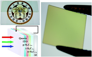
All silicon-rich silicon carbide (Si-rich SixC1−x)-based single p–i–n junction photovoltaic solar cells (PVSCs) were fabricated by growing nonstoichiometric Si-rich SixC1−x films through medium-temperature hydrogen-free plasma enhanced chemical vapor deposition. The Si-rich SixC1−x-based thin-film p–i–n junction PVSCs exhibit improved power conversion efficiency when an intrinsic Si-rich SixC1−x absorbing layer with a low C/Si composition ratio is added; amorphous Si (a-Si) particles are embedded in this absorbing layer. Lowering the [CH4]/[CH4 + SiH4] fluence ratio from 0.5 to 0.3 reduces the C/Si composition ratio of Si-rich SixC1−x films from 0.74 to 0.665. The absorbance of these films in the visible light region (400–800 nm) is substantially enhanced to 3.8 × 105 cm−1 by reducing the [CH4]/[CH4 + SiH4] fluence ratio, which is up to one order of magnitude larger than that of crystalline Si. The open-circuit voltage and short-circuit current density of the indium tin oxide/p-SixC1−x/i-SixC1−x/nSixC1−x/Al PVSCs are enhanced to 0.51 V and to 19.7 mA cm−2, respectively, raising the conversion efficiency and filling factor to 2.24% and 0.264, respectively. Through hydrogen-free deposition of the Si-rich SixC1−x p–i–n cells on a-Si based p–i–n cells, Si-rich SixC1−x/a-Si hybrid tandem PVSCs exhibit enhanced conversion efficiency and an enhanced filling factor of 6.47% and 0.332, respectively.
1. Introduction
Amorphous nonstoichiometric silicon carbide (a-SixC1−x) is an ideal candidate for optoelectronic applications because of its wide tunable optical bandgap and easy synthesis at low substrate temperatures.1–5 SixC1−x is usually employed as a window layer in solar cell applications to make conventional Si photovoltaic solar cells (PVSCs) perfect visible-blind p-type windows.6,7 Typically, stoichiometric SiC has low absorption coefficients in the visible light region and poor electrical properties even after doping.8,9 To overcome these drawbacks, nonstoichiometric SixC1−x with a tunable optical bandgap has been investigated in recent years; its electrical properties can be modified by varying the composition ratio, enabling its application as an absorbing layer in PVSCs.10,11 Through plasma enhanced chemical vapor deposition (PECVD), nonstoichiometric SixC1−x has been synthesized by varying growth parameters such as substrate temperature;12,13 this procedure is similar to the syntheses of nonstoichiometric SiOx and SiNx materials.14,15 The tunable optical bandgap of nonstoichiometric SixC1−x strongly depends on its C/Si composition, which further influences the absorption spectra.
During PECVD under hydrogen dilution, hydrogen carriers can reduce the density of defect states at the surface.16 However, fabrication under hydrogen dilution usually requires a high substrate temperature and RF plasma power.17–19 Under hydrogen-free PECVD, nonstoichiometric Si-rich SixC1−x can be synthesized at low substrate temperatures, considerably enhancing its absorption coefficient. Compared with crystalline Si (c-Si) films, nonstoichiometric Si-rich SixC1−x materials have been reported to have smaller optical bandgaps and higher absorption coefficients in the visible light region (400–600 nm).20 Many studies have reported the practical applications of a-Si and SixC1−x hybrid PVSCs.21–24 However, few reports have emphasized all SixC1−x-based PVSCs.6,20 Gao et al. applied SixC1−x-based n–i–p junction PVSCs as semitransparent solar cells in optical transmittance modulators, but reported a <1% conversion efficiency.6 Lee et al. reduced the thickness of n-type SixC1−x films from 150 to 25 nm for SixC1−x-based p–n junction PVSCs; such parametric tuning enhanced the conversion efficiency from 5 × 10⁻³% to 4.7%.20
In this study, an all SixC1−x-based single p–i–n junction semitransparent PVSC on a quartz substrate was demonstrated. Nonstoichiometric SixC1−x films were grown using anomalous hydrogen-free PECVD at a substrate temperature far lower than the SiC synthesis temperature of 1000 °C. The intrinsic SixC1−x (i-SixC1−x) films served as an absorbing layer of which the composition ratio can be tuned by varying the fluence ratios of silane (SiH4) and methane (CH4) during growth to improve the photocurrent response. In addition, Si-rich SixC1−x/a-Si tandem solar cells with i-SixC1−x layers of different C/Si composition ratios were fabricated and analyzed. To optimize the conversion efficiency of the Si-rich SixC1−x/a-Si tandem solar cells, the C/Si composition ratio of the n-a-SixC1−x layer was tuned by modifying the fluence ratio of SiH4 and CH4 during growth, increasing the tunneling probability at the n-a-SixC1−x/p-a-Si interface.
2. Experimental
2.1 Synthesis of Si-rich SixC1−x films
Si-rich SixC1−x films were deposited on quartz substrates through medium-temperature hydrogen-free PECVD with varying Ar-diluted SiH4 and CH4 compositions. The chamber pressure, substrate temperature, and RF plasma power were maintained at 0.25 torr, 500 °C, and 100 W, respectively. During PECVD, the fluence ratio, defined as RSiC = [CH4]/[SiH4 + CH4], was varied from 0.3 to 0.5 in increments of 0.1, which facilitated tuning of the C/Si composition ratio of Si-rich SixC1−x films. When growing the p- and n-type contact layer for the SixC1−x PVSC, RSiC was maintained at 0.5. Additionally, Ar-diluted B2H6 and Ar-diluted PH3 (1%) fluence was set at 9 sccm and 140 sccm to fabricate the p- and n-type SixC1−x films, respectively. The C/Si composition ratio of the nonstoichiometric SixC1−x films was determined using X-ray photoelectron spectroscopy (XPS) with a Mg Kα radiation source at 1256.3 eV. Moreover, the optical transmittance and reflectance spectra of the Si-rich SixC1−x films ranging between 300 and 1200 nm were measured using a xenon light source (Oriel, 68147+68830) and a monochromator (CVI, DK240); these spectra are mandatory for deriving the absorption coefficient of the Si-rich SixC1−x films. The optical bandgap of the Si-rich SixC1−x films can be determined by modifying their measured transmittance and reflectance spectra.
2.2 Fabrication of a pure Si-rich SixC1−x PVSC and a hybrid SixC1−x/a-Si tandem PVSC
The configuration of the Si-rich SixC1−x single p–i–n junction PVSC is depicted in Fig. 1. The 25 nm thick p- and n-type Si-rich SixC1−x films with resistivities of 0.12 and 0.87 Ω cm, respectively, were deposited by doping the fixed reactant gas with additional B2H6 and PH3. The C/Si composition ratio of the tuned i-SixC1−x absorbing layers with a thickness of 25 nm was varied by tuning the RSiC. First, the p–i–n structure of the SixC1−x film was deposited on indium tin oxide (ITO) quartz substrates. Subsequently, thermally evaporated aluminum (Al) with a thickness of 200 nm was grown to form the ITO/p-SixC1−x/i-SixC1−x/n-SixC1−x/Al PVSCs.25 The current–voltage (I–V) characteristics of all PVSC devices under AM1.5G solar simulator irradiation were measured using a multimeter (Keithley 2420) and analyzed using homemade software. The a-Si based PVSCs were fabricated using a different inductively coupled PECVD system with the substrate temperature, chamber pressure, and RF plasma power density maintained at 140 °C, 0.7 torr, and 135 mW cm−2, respectively. The reacting gas fluence ratio, Ra-Si = [SiH4]/[H4] + [SiH4], was set at 9%, and the fluence ratios of the PH3 and B2H6 dopants in the gas mixture host were 5% and 13%, respectively. The p- and n-type a-Si films were 12 and 20 nm thick, respectively, and the i-a-Si film was maintained at a thickness of 400 nm. Fig. 2 exhibits the cross-sectional scanning electron microscopy (SEM) image of the Si-rich SixC1−x/a-Si tandem PVSC, in which the bottom layers are the p–i–n Si-rich SixC1−x and the top layers are the a-Si PVSCs. In addition, the Si-rich SixC1−x/a-Si tandem PVSC has a slight roughness with a reduced density of structural defects. This phenomenon eventually enlarges the shunt resistance of the device to further enhance its solar energy conversion efficiency. Surface roughening in some areas of the Si-rich SixC1−x/a-Si tandem PVSC is also observed, which increases the anti-reflective effect to prompt optical absorption.
 |
| Fig. 1 Schematic structure and photograph of a Si-rich SixC1−x-based single p–i–n junction semitransparent PVSC. | |
 |
| Fig. 2 Cross-sectional SEM image of the SixC1−x/a-Si tandem PVSC. Inset: schematic structure of the Si-rich SixC1−x/a-Si PVSC. | |
3. Results and discussion
3.1 XPS analysis of the composition of the Si-rich SixC1−x films
Fig. 3 shows the XPS spectra of Si-rich SixC1−x films grown at different RSiC. The C/Si composition ratio of the Si-rich SixC1−x films improves from 0.36 to 0.50 as RSiC increases from 0.3 to 0.5; this contributes to the molar fraction index X of the Si-rich SixC1−x films decreasing from 0.74 to 0.665, because of the enhanced C content in these films, which have a higher number of decomposed carbon atoms. At a low temperature and RF plasma power, because of the lower dissociation energy for SiH4 molecules (75.6 kcal mol−1), the SiH4 molecules are more easily decomposed than the CH4 molecules.26
 |
| Fig. 3 XPS spectra of Si-rich SixC1−x films grown at different RSiC. | |
With a higher SiH4 and CH4 molecule density in the PECVD chamber, the obtained energy of each reactant molecule from the plasma is sufficiently low that the SiH4 and CH4 molecule decomposition rates do not substantially differ. The increased dissociation energy of each reactant molecule at high deposition temperatures causes the SiH4 and CH4 molecule decomposition rates to differ from each other, especially when the total reactant fluence is lowered by increasing the RSiC. Therefore, Si-rich SixC1−x films with a high RSiC exhibit low excessive Si content, which eventually enhances the C/Si composition ratio.
In addition, the O/Si composition ratio of the Si-rich SixC1−x films increases from 4.9% to 6.4% as RSiC increases. Because the dissociation energy of oxygen molecules is 314.3 kcal mol−1, when the residual oxygen in the chamber is not completely purged, the residual O content in the Si-rich SixC1−x films exhibits an increasing trend similar to that of the C content. Specifically, the compositional bonds in the Si-rich SixC1−x films can be analyzed by deconvoluting the Si(2p)-orbital-electron-related XPS spectra, as shown in Fig. 4. These spectra are fitted by four separate Gaussian components with binding energies of 99.7, 110.5, 101.5, and 103.35 eV, which are attributed to the Si–Si, Si–C, C–Si–O, and O–Si–O bonds, respectively.1 The density of Si–Si bonds increases when the Si-rich SixC1−x films are grown at a low RSiC, which induces a red-shift phenomenon at the absorption edge. In addition, the diminishing O–Si–O and C–Si–O bond densities indicate that the invaded oxygen content decreases in Si-rich SixC1−x films when grown slowly at a low RSiC.
 |
| Fig. 4 Si(2p)-related XPS spectra of Si-rich SixC1−x films grown at different RSiC. | |
The results of XPS analyses of the compositional variation of the Si-rich SixC1−x films at five different points are shown in Fig. 5. Data for the central and the four edge points of the Si-rich SixC1−x films confirm the composition uniformity (see Table 1) of the synthesized Si-rich SixC1−x films. For example, in the Si-rich SixC1−x film grown at an RSiC of 0.5, the average C/Si composition ratios in different areas of the film are almost identical, with an average of 0.665 and a standard deviation as low as 0.17%.
 |
| Fig. 5 (a) Schematic characterizing the composition uniformity of Si-rich SixC1−x films by using XPS analyses at five different points. (b) XPS spectra at different points of the Si-rich SixC1−x film grown at an RSiC of 0.5. | |
Table 1 Atomic content (in percentage) and the molar fraction index (X) at different points of the Si-rich SixC1−x films grown at an RSiC of 0.5
Si-rich SixC1−x film grown at the RSiC of 0.5 |
Measured position |
Si (at%) |
C (at%) |
O (at%) |
X |
A |
63.8 |
32.1 |
4.1 |
0.665 |
B |
64.0 |
31.8 |
4.2 |
0.668 |
C |
63.6 |
32.0 |
4.4 |
0.665 |
D |
63.7 |
32.4 |
3.9 |
0.663 |
E |
63.9 |
32.3 |
3.8 |
0.664 |
Average |
63.8 ± 0.2 |
32.1 ± 0.3 |
4.1 ± 0.3 |
0.665 |
Standard deviation |
0.3% |
0.8% |
15% |
0.17% |
3.2 Band structure and absorption characteristics of the Si-rich SixC1−x films and cells
The absorption spectra of the Si-rich SixC1−x films synthesized at different RSiC values are shown in Fig. 6(a). The broadened absorption spectra of the Si-rich SixC1−x film exhibits the highest absorption coefficient of up to 3.8 × 105 cm−1 in the visible wavelength region between 400 and 600 nm when the RSiC is reduced to 0.3 during PECVD. Moreover, the absorption coefficient of these films in the red and near-infrared regions increases as RSiC decreases because the excessive Si–Si bonds in the films contribute to the enhanced absorbance. By contrast, the invaded oxygen content in the Si-rich SixC1−x films suppresses the absorption spectra and reduces the absorption coefficient. In comparison, c-Si has a larger absorption coefficient <365 nm. However, c-Si rapidly attenuates its absorption in the visible wavelength region between 400 and 800 nm. Numerically, the optical bandgap of the Si-rich SixC1−x films can be evaluated by fitting Tauc’s equation: (αhν)0.5 = B(hν − Eg,opt), where h, ν, α and Eg,opt are Planck’s constant, frequency, absorption coefficient, and optical bandgap of the Si-rich SixC1−x films, respectively.10 The optical bandgap of the films substantially improves from 1.45 to 1.85 eV because of the increased C content in Si-rich SixC1−x films grown at an increased RSiC, as shown in Fig. 6(b). These results reveal that the absorption coefficient and optical bandgap of the Si-rich SixC1−x films are strongly dependent on the C/Si composition ratio of the films.
 |
| Fig. 6 (a) Absorption spectra and (b) Tauc plots of c-Si and Si-rich SixC1−x films grown at different RSiC. | |
Fig. 7 illustrates the band structure of the Si-rich SixC1−x/a-Si:H tandem PVSCs, which possesses a large interfacial barrier between the Si-rich SixC1−x and a-Si cells. Generally, such barriers degrade the carrier transportation and conversion efficiency of PVSCs. A possible carrier transportation route can be attained by enhancing electron tunneling in the conduction band and hole tunneling in the valence band by reducing the donor ionization energy (Edonor) between the donor level and the conduction band in the SixC1−x layer; the tunneling probability can be further improved by reducing the thickness of both the n-a-SiC and p-a-Si:H layers at the interface. Typical Edonor values of the P-doped 6H-SiC and Si are 0.135 and 0.045 eV, respectively,27 and the acceptor ionization energies (Eacceptor) of the B-doped 6H-SiC and Si are 0.27 eV and 0.045 eV, respectively.28 Therefore, the most feasible approach for tuning the Edonor and Eacceptor of SiC is to synthesize n-type Si-rich SixC1−x films with higher excessive Si content, thereby effectively reducing Edonor from 0.135 to 0.045 eV; thus, the energy discontinuity between the conduction band of the n-type Si-rich SixC1−x and p-type a-Si materials at the cell interface is considerably reduced from 0.18 to 0.09 eV (in the best case).
 |
| Fig. 7 Band structure of Si-rich SixC1−x/a-Si tandem PVSCs. | |
In the experiment, by reducing the C/Si composition ratio of the n-type a-SixC1−x film by lowering the RSiC during PECVD to obtain a high Si content, the Edonor of the n-a-SixC1−x film is reduced to enhance the tunneling probability at the n-a-SixC1−x/p-a-Si interface. The n-a-SixC1−x film with a lower C/Si composition ratio exhibits a lower optical bandgap and lower resistivity to hole barrier height reduction, thus providing another factor that enhances the tunneling probability at the n-a-SixC1−x/p-a-Si interface. This approach eventually reduces the series resistance of the Si-rich SixC1−x/a-Si tandem PVSC to further improve its overall conversion efficiency.
3.3 Photocurrent simulation of Si-rich SixC1−x-based PVSCs
Photocurrent density spectra of the Si-rich SixC1−x based PVSCs can be simulated using their absorption spectra because the excited electrons and holes are separated by the built-in voltage within a certain optical penetration depth. Theoretically, the photocurrent density spectra can be expressed as Isc(λ) = qAγα(λ)Φ0(λ)e−α(λ)z(Ln + Lp), where q is the electron charge, A is the active area of the Si-rich SixC1−x-based PVSCs, γ is the external quantum efficiency, Φ0(λ) is the flux density of the AM1.5G solar simulator, α(λ) is the absorption of the Si-rich SixC1−x films, z is the thickness of the films, and Ln and Lp are the diffusion lengths of the minority carriers in the neutral region. The photocurrent density spectra of the Si-rich SixC1−x-based PVSCs simulated assuming that Ln and Lp are 83 and 93 μm, respectively, and under AM1.5G irradiation, are shown in Fig. 8(a). The photocurrent density of these PVSCs with an i-SixC1−x absorbing layer exhibits a broader spectrum when grown at a lower RSiC because absorption is broadened to the near-infrared region; the excessive Si content in the films grown at a lower RSiC reduces the bandgap energy and enhances their near-infrared absorption from the visible to the near-infrared wavelengths. As shown in the normalized photocurrent spectra in Fig. 8(b), the enhanced absorption from the green to the infrared region results in more electron–hole pairs, increasing the conversion efficiency.
 |
| Fig. 8 (a) Photocurrent spectra of Si-rich SixC1−x films grown at different RSiC under AM1.5G irradiation. (b) Normalized photocurrent spectra of Si-rich SixC1−x films grown at different RSiC under AM1.5G irradiation. (c) Simulated photocurrent density of Si-rich SixC1−x films grown at different RSiC under AM1.5G irradiation. | |
Numerically, the short-circuit current density (JSC) of the Si-rich SixC1−x-based PVSCs can be calculated by integrating their photocurrent density spectra:29
|
 | (1) |
Eqn (1) reveals that the total JSC of the Si-rich SixC1−x-based PVSCs improves from 9.8 to 28.6 mA cm−2 when the RSiC is reduced from 0.5 to 0.3, as shown in Fig. 8(c). By enriching the Si content in the SiC matrix, the simulated JSC can be enhanced nearly threefold. Ideally, broadening the absorbance of the film grown at a lower RSiC from the green to the near-infrared region leads to photocurrent enhancement only. Nevertheless, when growing a single SixC1−x p–i–n cell, the p-type SixC1−x must be grown at a higher RSiC to prevent photoexcited carrier generation in the contact region; the n-type SixC1−x grown at a higher RSiC is a window layer, where the first reflected light enhances a second absorbance in the i-SixC1−x layer. This inevitably magnifies the series resistance of the entire cell. That is, the practical JSC of Si-rich SixC1−x-based PVSCs may be lower than the simulated density because the high series and low shunt resistances in the PVSCs hinder the transportation of excited carriers, consequently reducing the filling factor and degrading the solar energy conversion efficiency.
3.4 The performance of Si-rich SixC1−x-based PVSCs
3.4.1 All Si-rich SixC1−x-based PVSC. Si-rich SixC1−x-based PVSCs with an ITO/p-SixC1−x/i-SixC1−x/n-SixC1−x/Al structure were characterized under AM1.5G irradiation. The depletion widths in the n- and p-type regions were concurrently suppressed by improving the doping content in n- and p-SixC1−x, effectively reducing photocurrent generation. In this case, an i-SixC1−x absorbing layer can be added to broaden the absorption region in order to enhance photocurrent generation and consequently the conversion efficiency.30 However, this absorbing layer induces additional series resistance, which increases the open-circuit voltage (VOC) but degrades the filling factor of the PVSCs. Therefore, the absorbing layer plays a critical role in optimizing the conversion efficiency of Si-rich SixC1−x-based PVSCs.The I–V responses under AM1.5G irradiation of such PVSCs with an i-SixC1−x absorbing layer grown at different RSiC are shown in Fig. 9. When the RSiC is reduced from 0.5 to 0.3, the VOC and JSC of the PVSCs are enhanced from 0.47 to 0.51 V and from 14.1 to 19.7 mA cm−2, respectively, yielding an enhanced conversion efficiency and filling factor of 2.24% and 0.264, respectively, as listed in Table 2. The enhanced JSC corresponds to the broadened green and near-infrared absorbance of the Si-rich SixC1−x films grown at a low RSiC. Because of the excessive Si content in these films, the i-SixC1−x absorbing layers with low C/Si composition ratios offer lower series resistance, which causes the material characteristics of the films to approximate those of amorphous Si. This phenomenon effectively enhances the visible-infrared absorbance and suppresses the resistivity of the entire Si-rich SixC1−x film. The I–V response of the Si-rich SixC1−x-based PVSCs is atypical of the standard PVSC response because of the lower shunt resistance, which reduces the VOC of the fabricated PVSCs. The highest conversion efficiency among the fabricated PVSCs was obtained with the optimized i-SixC1−x absorbing layer grown at an RSiC of 0.3. The optimization of these PVSCs is attributed to the enhanced absorbance and decreased series resistance of the i-SixC1−x layer, which enhances both the filling factor and the conversion efficiency.
 |
| Fig. 9 I–V curves under AM1.5G irradiation of Si-rich SixC1−x-based PVSCs with the i-SixC1−x absorbing layer grown at different RSiC. Inset: schematic structure of the Si-rich SixC1−x-based PVSCs. | |
Table 2 PVSC parameters of the Si-rich SixC1−x-based PVSCs with the i-SixC1−x absorbing layer grown at different RSiC
Si-rich SixC1−x solar cell |
RSiC |
VOC (V) |
JSC (mA cm−2) |
F.F. |
PCE (%) |
0.3 |
0.51 |
19.7 |
0.264 |
2.24 |
0.4 |
0.49 |
18.5 |
0.261 |
1.95 |
0.5 |
0.47 |
14.1 |
0.255 |
1.70 |
Previous studies have employed n-type SiC as a top window and contact layer for a-Si-based PVSCs; n-type SiC with a large bandgap is preferred because it prevents inutile electron–hole pair generation. To enhance the conversion efficiency of the fabricated all Si-rich SixC1−x-based single p–i–n PVSC with a bottom Al-based reflective contact layer, the n-type SixC1−x layer grown at a higher RSiC must exhibit a higher bandgap to avoid optoelectronic conversion in the n-type SixC1−x layer, which ideally can increase the filling factor and enhance the conversion efficiency because of the second absorbance in the i-SixC1−x layer. However, the higher bandgap of the n-type SixC1−x layer induces an interfacial barrier which reduces carrier transportation at the interface between the n-type SixC1−x and the p-type a-Si when forming the SixC1−x- and a-Si-based dual-cell PVSC, eventually increasing the series resistance of Si-rich SixC1−x-based PVSCs, as elaborated in the following section.
3.4.2 Hybrid Si-rich SixC1−x/a-Si and a-Si tandem PVSC. To characterize the overall performance of the Si-rich SixC1−x/a-Si cell hybrid and compare it with that of other PVSCs, a pure a-Si-based PVSC was initially analyzed. Fig. 10 shows that the VOC and JSC of the a-Si solar cell are 0.43 V and 14 mA cm−2, respectively, yielding a conversion efficiency of 3.97% and a filling factor of 0.66. Subsequently, the hybrid Si-rich SixC1−x/a-Si tandem PVSC with the a-Si PVSC functioning as the bottom cell was fabricated to characterize the enhancement in power conversion efficiency.
 |
| Fig. 10 I–V curve of a-Si-based PVSC under AM1.5G irradiation. Inset: schematic structure of the a-Si-based PVSC. | |
As plotted in Fig. 11, the I–V responses under AM1.5G irradiation reveal that the conversion efficiency of the tandem solar cells can be considerably enhanced by optimizing the C/Si composition ratio of the i-SixC1−x absorbing layer in the upper Si-rich SixC1−x cell. When the RSiC is reduced from 0.5 to 0.3 for synthesizing the i-a-SixC1−x absorbing layer, the VOC and JSC of the tandem solar cell rise to 0.85 V and 18.9 mA cm−2, respectively, increasing the filling factor and the conversion efficiency to optimal values of 0.301 and 6.17%, respectively.
 |
| Fig. 11 I–V curves under AM1.5G irradiation of Si-rich SixC1−x/a-Si PVSCs with the i-SixC1−x absorbing layer grown at different RSiC. Inset: schematic structure of the Si-rich SixC1−x/a-Si PVSCs. | |
After annealing, the filling factor and conversion efficiency of the SixC1−x/a-Si tandem solar cell further improve to 0.332 and 6.47%, respectively, as shown in Fig. 12. A lower RSiC during the i-SixC1−x synthesis apparently reduces series resistance and raises the shunt resistance of the Si-rich SixC1−x/a-Si p–i–n cell, as shown in the forward and the reverse bias regions of the I–V plot. These results confirm that the i-SixC1−x with a lower C/Si composition ratio enhances the overall performance of the hybrid Si-rich SixC1−x/a-Si tandem PVSC, which possesses higher photocurrent productivity than those of single PVSCs, including the purely single Si-rich SixC1−x and single a-Si PVSCs.
 |
| Fig. 12 I–V curves under AM1.5G irradiation of the annealed Si-rich SixC1−x/a-Si PVSCs with the i-SixC1−x absorbing layer grown at different RSiC. Inset: schematic structure of the annealed Si-rich SixC1−x/a-Si PVSCs. | |
The obtained results indicate that, in addition to tuning the C/Si composition ratio of the i-SixC1−x layer, other possible modifications warrant investigation. For example, varying the C/Si composition ratio and the film thickness of the n-type SixC1−x layer is critical in enhancing the conversion efficiency of hybrid Si-rich SixC1−x/a-Si tandem PVSCs. Reducing the thickness of the n-type SixC1−x layer can increase the tunneling probability at the n-a-SixC1−x/p-a-Si interface. Moreover, this design can effectively reduce the series resistance of the entire tandem cell. Furthermore, the lowered C/Si composition ratio of the n-type SixC1−x film not only raises the tunneling probability at the n-a-SixC1−x/p-a-Si interface but also reduces the lattice constant mismatch between the n-type SixC1−x and p-a-Si films, thereby increasing the shunt resistance of Si-rich SixC1−x/a-Si tandem PVSCs. Therefore, appropriate tuning of the C/Si composition ratio and the film thickness of the n-type SixC1−x layer can be investigated to further improve the device performance of these tandem PVSCs.
4. Conclusions
Si-rich SixC1−x films grown at different RSiC fluence ratios were applied as an i-SixC1−x absorbing layer in all Si-rich SixC1−x-based PVSCs. Lowering the RSiC from 0.5 to 0.3 reduced the C/Si composition ratio of these films from 0.503 to 0.36, because of the difference in dissociation energy between CH4 and SiH4 molecules. A lower RSiC during PECVD facilitates the growth of Si-rich SixC1−x films with smaller C/Si composition ratios, affording higher absorption coefficients and smaller optical bandgaps. The Si-rich Si0.74C0.26 film with the smallest optical bandgap of 1.45 eV yielded a large absorption coefficient of 3.8 × 105 cm−1 in the visible wavelength region (400–600 nm). A higher excessive Si content in Si-rich SixC1−x films broadens absorbance in the red and near-infrared regions. When the RSiC is varied from 0.5 to 0.3, the VOC and JSC of Si-rich SixC1−x-based PVSCs are enhanced from 0.47 to 0.51 V and from 14.1 to 19.7 mA cm−2, respectively, providing a conversion efficiency and filling factor of 2.24% and 0.264, respectively. The performance of the Si-rich SixC1−x-based PVSCs is enhanced because of the stronger absorbance and decreased series resistance of the i-SixC1−x absorbing layer. When the i-SixC1−x layer is grown at a decreased RSiC of 0.3, the Si-rich SixC1−x/a-Si tandem PVSC offers a VOC and JSC of 0.85 V and 18.9 mA cm−2, respectively, optimizing the filling factor and conversion efficiency to 0.301 and 6.17%, respectively. After annealing, the filling factor and conversion efficiency of these solar cells can be further improved to 0.332 and 6.47%, respectively. These results confirm that i-SixC1−x with lower C/Si composition ratios exhibit improved performance, enabling hybrid Si-rich SixC1−x/a-Si tandem PVSCs to deliver higher photocurrents than those with stoichiometric and C-rich compositions. Thus, Si-rich SixC1−x films can be considered not only a window layer but also an absorbing layer in Si-based PVSCs.
Acknowledgements
This work was financially supported by the Ministry of Science and Technology, Taiwan, R.O.C. and the Excellent Research Projects of National Taiwan University, Taiwan, R.O.C., under grants NSC 101-2221-E-002-071-MY3, MOST 103-2221-E-002-042 -MY3 and 103R89083.
Notes and references
- C.-H. Cheng, C.-L. Wu, C.-C. Chen, L.-H. Tsai, Y.-H. Lin and G.-R. Lin, Si-rich SixC1−x light-emitting diodes with buried Si quantum dots, IEEE Photonics J., 2012, 4, 1762–1775 CrossRef.
- P.-K. Chang, P.-T. Hsieh, C.-H. Lu, C.-H. Yeh and M.-P. Houng, Development of high efficiency p–i–n amorphous silicon solar cells with the p-mc-Si:H/p-a-SiC:H dual window layer, Sol. Energy Mater. Sol. Cells, 2011, 95, 2659–2663 CrossRef CAS PubMed.
- B.-S. Song, S. Yamada, T. Assno and S. Noda, Demonstration of two-dimensional photonic crystals based on silicon carbide, Opt. Express, 2011, 19, 11084–11089 CrossRef CAS PubMed.
- Y. Qu, V. Jokubavicius, P. Hens, M. Kaiser, P. Wellmann, R. Yakimova, M. Syväjärvi and H. Qu, Broadband and omnidirectional light harvesting enhancement of fluorescent SiC, Opt. Express, 2012, 20, 7575–7579 CrossRef PubMed.
- D. Song, E.-C. Cho, G. Conibeer, C. Flynn, Y. Huang and M. A. Green, Structural, electrical and photovoltaic characterization of Si nanocrystals embedded SiC matrix and Si nanocrystals/c-Si heterojunction devices, Sol. Energy Mater. Sol. Cells, 2008, 92, 474–481 CrossRef CAS PubMed.
- W. Gao, S. H. Lee, J. Bullock, Y. Xu, D. K. Benson, S. Morrison and H. M. Branz, First a-SiC:H photovoltaic-powered monolithic tandem electrochromic smart window device, Sol. Energy Mater. Sol. Cells, 1999, 59, 243–254 CrossRef CAS.
- S. J. Baik, S. J. Kang and K. S. Lim, Extraction of carriers photogenerated at p type amorphous SiC window layer in amorphous Si solar cells, Appl. Phys. Lett., 2010, 97, 12202 Search PubMed.
- A. Orpella, M. Vetter, R. Ferré, I. Martiń, J. Puigdollers, C. Voa and R. Alcubilla, Phosphorus-diffused silicon solar cell emitters with plasma enhanced chemical vapour deposited silicon carbide, Sol. Energy Mater. Sol. Cells, 2005, 87, 667–674 CrossRef CAS PubMed.
- F. Demichelis, C. G. Pirri and E. Tresso, Influence of doping on the structural and optoelectronic properties of amorphous and microcrystalline silicon carbide, J. Appl. Phys., 1992, 72, 1327–1333 CrossRef CAS PubMed.
- G.-R. Lin, T.-C. Lo, L.-H. Tsai, Y.-H. Pai, C.-H. Cheng, C.-I. Wu and P.-S. Wang, Finite silicon atom diffusion induced size limitation on self-assembled silicon quantum dots in silicon-rich silicon carbide, J. Electrochem. Soc., 2011, 159, K35–K41 CrossRef PubMed.
- T.-C. Lo, L.-H. Tsai, C.-H. Cheng, P.-S. Wang, Y.-H. Pai and G.-R. Lin, Self-aggregated Si quantum dots in amorphous Si-rich SiC, J. Non-Cryst. Solids, 2012, 358, 2126–2129 CrossRef CAS PubMed.
- Q. J. Cheng, E. Tam, S. Xu and K. Ostrikov, Si quantum dots embedded in an amorphous SiC matrix: nanophase control by non-equilibrium plasma hydrogenation, Nanoscale, 2010, 2, 594–600 RSC.
- Q. J. Cheng, S. Xu, J. Long, S. Huang and J. Guo, Homogeneous nanocrystalline cubic silicon carbide films prepared by inductively coupled plasma chemical vapor deposition, Nanotechnology, 2007, 18, 465601 CrossRef PubMed.
- G.-R. Lin, C.-J. Lin and C.-K. Lin, Oxygen defect and Si nanocrystals dependent white-light and near-infrared electroluminescence of Si-implanted and plasma-enhanced chemical vapor deposition-grown Si-rich SiOx, J. Appl. Phys., 2005, 94, 094306 CrossRef PubMed.
- C.-D. Lin, C.-H. Cheng, Y.-H. Lin, C.-L. Wu, Y.-H. Pai and G.-R. Lin, Comparing retention and recombination of electrically injected carriers in Si quantum dots embedded in Si-rich SiNx, Appl. Phys. Lett., 2011, 99, 243501 CrossRef PubMed.
- T. Kunii, T. Honda, N. Yoshida and S. Nonomura, Optical properties of microcrystalline 3C-SiC:H films measured by resonant
photochemicalbending spectroscopy, J. Non-Cryst. Solids, 2006, 352, 1196–1199 CrossRef CAS PubMed.
- C.-H. Cheng, P.-S. Wang, C.-I. Wu and G.-R. Lin, Nano-crystalline silicon-based bottom gate thin-film transistor grown by LTPECVD with hydrogen-free He diluted SiH4, J. Disp. Technol., 2013, 10, 814–820 CrossRef.
- A. Parashar, S. Kumar, J. Gope, C. M. S. Routhan, P. N. Dixit and S. A. Hashmi, Influence of argon dilution on growth and properties of hydrogenated nanocrystalline silicon films, Sol. Energy Mater. Sol. Cells, 2010, 94, 892–899 CrossRef CAS PubMed.
- G.-R. Lin, Y.-H. Pai and C.-T. Lin, Microwatt MOSLED using SiOx with buried Si nanocrystals on Si nano-pillar array, J. Lightwave Technol., 2008, 26, 1486–1491 CrossRef CAS.
- C.-T. Lee, L.-H. Tsai, Y.-H. Lin and G.-R. Lin, A chemical vapor deposited silicon rich silicon carbide p–n junction based thin-film photovoltaic solar cell, ECS J. Solid State Sci. Technol., 2012, 1, Q144–Q148 CrossRef CAS PubMed.
- I. A. Yunaz, K. Hashizume, S. Miyajima, A. Yamada and M. Konagai, Fabrication of amorphous silicon carbide films using VHF-PECVD for triple-junction thin-film solar cell applications, Sol. Energy Mater. Sol. Cells, 2009, 93, 1056–1061 CrossRef CAS PubMed.
- I. A. Yunaz, H. Nagashima, D. Hamashita, S. Miyajima and M. Konagai, Wide-gap a-SixC1−x:H solar cells with high light-induced stability for multijunction structure applications, Sol. Energy Mater. Sol. Cells, 2011, 95, 107–110 CrossRef CAS PubMed.
- M. Abdelkrim, M. Loulou, R. Gharbi, M. Fathallah, C. F. Pirri and E. Tresso, Static and dynamic electrical study of a-SiC:H based p–i–n structure, effect of hydrogen dilution of the intrinsic layer, Solid-State Electron., 2007, 51, 159–163 CrossRef CAS PubMed.
- Y. Tawada, M. Kondo, H. Okamoto and Y. Hamakawa, Hydrogenated amorphous silicon carbide as a window material for high efficiency a-Si solar cells, Sol. Energy Mater., 1982, 6, 299–315 CrossRef CAS.
- W.-L. Hsu, Y.-H. Pai, F.-S. Meng and G.-R. Lin, Nanograin crystalline transformation enhanced UV transparency of annealing refined indium tin oxide, Appl. Phys. Lett., 2009, 94, 231906 CrossRef PubMed.
- F. Demichelis, C. F. Pirri and E. Tresso, Influence of doping on the structural and optoelectronic properties of amorphous and microcrystalline silicon carbide, J. Appl. Phys., 1992, 72, 1327–1333 CrossRef CAS PubMed.
- A. A. Lebedev, Deep level centers in silicon carbide: A review, Semiconductors, 1999, 33, 107–130 CrossRef CAS.
- A. O. Evwaraye, S. R. Smith, W. C. Mitchel and H. M. Hobgood, Boron acceptor levels in 6H-SiC bulk samples, Appl. Phys. Lett., 1997, 71, 1186–1188 CrossRef CAS PubMed.
- C.-H. Cheng, Y.-H. Lin, J.-H. Chang, C.-I. Wu and G.-R. Lin, Semi-transparent Si-rich SixC1−x p–i–n photovoltaic solar cell grown by hydrogen-free PECVD, RSC Adv., 2014, 4, 18397–18405 RSC.
- Y. Tawada, H. Okamoto and Y. Hamakawa, a-SiC:H/a-Si:H heterojunction solar cell having more than 7.1% conversion efficiency, Appl. Phys. Lett., 1981, 39, 237 CrossRef CAS PubMed.
|
This journal is © The Royal Society of Chemistry 2015 |
Click here to see how this site uses Cookies. View our privacy policy here.