
Synthesis, characterization and gas sensing properties of porous flower-like indium oxide nanostructures
Xiumei Xuab,
Xin Lia,
Haijiao Zhangc,
Changhao Fenga,
Chong Wanga,
Fangmeng Liua,
Yanfeng Sun*a,
Peng Suna and
Geyu Lu*a
aState Key Laboratory on Integrated Optoelectronics, College of Electronic Science and Engineering, Jilin University, Changchun 130012, China. E-mail: lugy@jlu.edu.cn; syf@jlu.edu.cn; Tel: +86 431 85167808
bCollege of Physics and Electronic Engineering, Nanyang Normal University, Nanyang 473061, China
cCollege of Chemistry and Pharmaceutical Engineering, Nanyang Normal University, Nanyang 473061, China
First published on 16th March 2015
Abstract
In this work, flower-like In2O3 nanostructures were prepared with a solvothermal method in the presence of K3C6H5O7·H2O. The as-synthesized samples were characterized by using X-ray powder diffraction (XRD), field emission scanning electron microscopy (FESEM), and transmission electron microscopy (TEM). The results indicate that the synthesized flower-like In2O3 nanostructures were constructed by porous nanosheets. The gas sensing properties of the as-obtained products were investigated. It was found that the sensor based on such flower-like In2O3 nanostructures exhibited high response and good selectivity to NO2.
1. Introduction
The properties and applications of nanostructured materials are known to have close relationships with their morphology, size, structure, and chemical composition.1–3 To date, a wide variety of functional materials with hierarchical structure can provide many opportunities for exploring novel properties and superior device performances, due to their higher specific area and peculiar characteristics compared to solid structures. Hence, over the past decade, many research groups have focused on controlling the morphology of inorganic nanostructures. In this respect, hierarchical self-assembly structures from nanosized building blocks with specific morphology have attracted considerable interest for their potential applications. To synthesize the complex architectures, various strategies have been employed successfully to assemble building blocks into hierarchical architectures based on different driving mechanisms.4–6 To realize the short diffusion lengths of the target gases and the large sensing material/gas contact area, different structures have been designed, such as hollow structures, flower-like structures, and hierarchical structures.As a very important wide-band-gap (direct band gap around 3.6 eV) n-type semiconductor, In2O3 has been recognized as a promising semiconductor material for gas sensor, window heaters, solar cells, liquid-crystal displays7–16 due to its nontoxicity, low cost, and excellent stability. Among most of the potential applications, the morphology and structure of the nanomaterials will undoubtedly play the pivotal role in determining their properties. In order to improve the performance of devices based on In2O3, various morphologies of In2O3 with different dimensional nanostructures, such as nanoplates, nanowires, nanobelts, nanotubes, nanocubes, nanofibers, nanosheets and complex hierarchical structures constructed with nanoscale building blocks, have been synthesized via a series of routes.17–26 To date, many types of hierarchical superstructures have been successfully fabricated by a variety of methods, including vapor–liquid–solid (VLS), solution–liquid–solid (SLS) phase catalytic growth, and anisotropic growth of crystalline nano-materials using proper capping agents to fabricate nanostructures with the desired architectures. However, these methods usually hold disadvantages related to high temperatures or tedious synthetic procedures, which possibly result in the increased cost and limit the potential applications. Therefore, exploration of a simple, mild and economical approach is strongly desirable for the fabrication of hierarchical nanostructures. Nevertheless, in spite of extensive research efforts, synthesis of hierarchical structures by a simple solvothermal route still remains a technological challenge.
Herein, we report a facile method for the preparation of hierarchical In2O3 by a simple solvothermal process. The obtained flower-like In2O3 hierarchical architectures consisted of nanosheets. Gas-sensing properties of the as-obtained In2O3 products were also investigated. The as-obtained flower-like In2O3 samples exhibited a high gas-sensing sensitivity for NO2, making them promising candidates for practical detectors for NO2.
2. Experimental
2.1. Synthesis and characterization of flower-like In2O3
All the reagents (analytical-grade purity) were used without any further purification. In a typical synthesis, 0.381 g of In(NO3)3·4.5H2O and 0.05 g K3C6H5O7·H2O were added to 32 mL of ethanol to form a homogeneous solution. After being stirred and ultrasonically treated alternately, 4 mL of water was added into the above mixed solution under vigorous stirring. The mixed solution was transferred to a Teflon-lined stainless steel autoclave, sealed tightly, and maintained at 160 °C for 12 h. After the autoclave was cooled to room temperature naturally, the precipitates were washed with deionized water and absolute ethanol for several times using centrifuge, and then dried at 80 °C for 24 h. The precipitates were sintered at 550 °C for 2 h in a muffle furnace. After the samples were cooled to room temperature, the flower-like In2O3 nanostructures were obtained.X-ray power diffraction (XRD) analysis was conducted on a Rigaku D/max-2500 X-ray diffractometer with Cu Kα1 radiation (λ = 1.5405 Å) in the range of 20–70°. The mean crystallite size was calculated using the Debye–Scherrer formula, D = 0.89λ/(β![[thin space (1/6-em)]](https://www.rsc.org/images/entities/char_2009.gif) cosθ), where λ is the X-ray wavelength, θ is the Bragg diffraction angle and β is the peak width at half maximum. The specific surface area was estimated using the Brunauer–Emmett–Teller (BET) equation based on the nitrogen adsorption isotherm obtained with a Micromeritics Gemini VII apparatus (surface area and porosity system). Samples were degassed under vacuum at 200 °C for 8 h prior to the measurements. The pore size distribution was determined with the Barrett–Joyner–Halenda (BJH) method applied to the desorption branch of adsorption–desorption isotherm. Field emission scanning electron microscopy (FESEM) images were recorded on a JEOL JSM-7500F microscope operating at 15 kV. Transmission electron microscopy (TEM), selected-area electron diffraction (SAED), and high-resolution transmission electron microscopy (HRTEM) measurements were obtained on a JEOL JEM-2100 microscope operated at 200 kV.
cosθ), where λ is the X-ray wavelength, θ is the Bragg diffraction angle and β is the peak width at half maximum. The specific surface area was estimated using the Brunauer–Emmett–Teller (BET) equation based on the nitrogen adsorption isotherm obtained with a Micromeritics Gemini VII apparatus (surface area and porosity system). Samples were degassed under vacuum at 200 °C for 8 h prior to the measurements. The pore size distribution was determined with the Barrett–Joyner–Halenda (BJH) method applied to the desorption branch of adsorption–desorption isotherm. Field emission scanning electron microscopy (FESEM) images were recorded on a JEOL JSM-7500F microscope operating at 15 kV. Transmission electron microscopy (TEM), selected-area electron diffraction (SAED), and high-resolution transmission electron microscopy (HRTEM) measurements were obtained on a JEOL JEM-2100 microscope operated at 200 kV.
2.2. Fabrication and measurement of sensor
Gas sensors were fabricated as follows: the as-obtained powder was mixed with the deionized water in order to make a paste, which was coated onto an alumina tube (4 mm in length, 1.2 mm in external diameter, and 0.8 mm in internal diameter, attached with a pair of gold electrodes) by a small brush to form a film. After drying at room temperature for 30 min, the sensing devices were sintered at 550 °C for 2 h. A pair of gold electrodes was installed at each end of the ceramic tube before it was coated with the paste, and each electrode was connected with two Pt wires. A Ni–Cr heating wire was inserted into the tube to form an indirect-heated gas sensor. The structure of the sensor is shown in Fig. 1.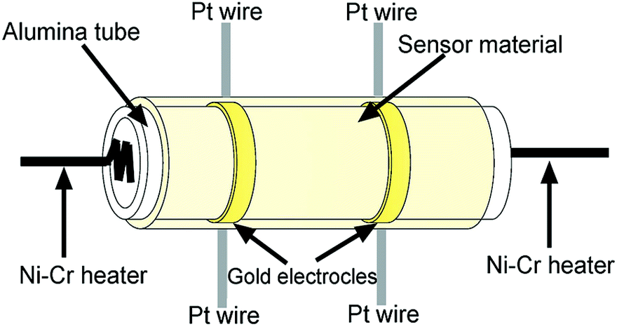 | ||
| Fig. 1 Schematic structure of the gas sensor. | ||
The electrical properties of the sensor were measured by CGS-8 intelligent test meter (Beijing Elite Tech. Co., Ltd, China). The response of the sensor was defined as S = Rg/Ra for oxidizing gas or Ra/Rg for reducing gas, here, Ra and Rg were the resistances of the sensor in the air and target gas, respectively. The response time is defined as the time required for the variation in resistance to reach 90% of the equilibrium value after a test gas was injected, and the recovery time is the time necessary for the sensor to return to 10% above the original resistance in air after releasing the test gas.
3. Results and discussion
3.1. Structural and morphological characteristics of the obtained In2O3
Fig. 2 shows the X-ray powder diffraction (XRD) pattern of the calcined product. The diffraction peaks can be indexed to a rhombohedral structure of In2O3 according to JCPDS card no. 21-406, with space group R![[3 with combining macron]](https://www.rsc.org/images/entities/char_0033_0304.gif) c (no. 167) and lattice parameters of a = 5.49 Å and c = 14.52 Å. The mean crystallite size of In2O3 was calculated to be around 20 nm using the Debye–Scherrer formula.
c (no. 167) and lattice parameters of a = 5.49 Å and c = 14.52 Å. The mean crystallite size of In2O3 was calculated to be around 20 nm using the Debye–Scherrer formula.
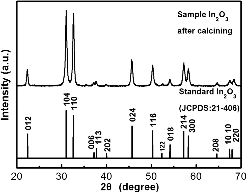 | ||
| Fig. 2 X-ray diffraction patterns of as-obtained In2O3 samples. | ||
The morphology of the samples was investigated by field emission scanning electron microscopy (FESEM). Fig. 3a–c shows typical FESEM images of the samples In2O3 at different magnifications. The low magnification FESEM image (Fig. 3a) clearly displayed that the products are composed of flower-like nanostructures. The detailed morphology information about In2O3 is presented in an enlarged-magnification FESEM (Fig. 3b), indicating that such flower-like nanostructures are built from nanosheets. It can be observed that the edge thickness of nanosheets is about 20 nm. Moreover, nanometre-sized porous architectures were formed in the nanosheets, as shown in Fig. 3c. On the basis of the above results, the as-obtained flower-like structure can be generally classified as hierarchical structures. The EDX of the products, shown in Fig. 3d, indicates that the obtained In2O3 are composed of only three elements: In, O, and Si (Si from the Si substrate used for SEM measurement).
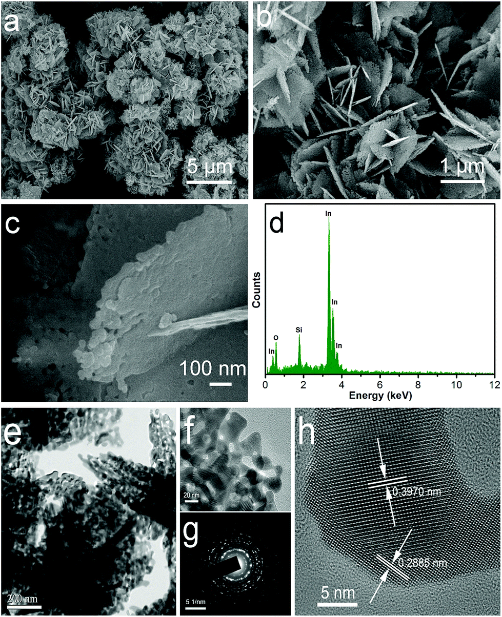 | ||
| Fig. 3 FESEM images of the as-obtained In2O3 structure: (a) a panoramic and (b) an enlarged of a part of samples. (c) A high-magnification FESEM image of an individual flower-like In2O3. (d) The EDX pattern of In2O3. (e) Typical TEM images of as-obtained In2O3 nanostructures. (f) An individual porous In2O3 nanosheet. (g) The corresponding SAED pattern. (h) HRTEM images taken from (e and f). | ||
Further detailed structural analysis of flower-like samples was carried out using TEM. Fig. 3e and f shows the TEM image of flower-like In2O3 nanostructures. It can be seen that the size and shape of product were similar to those of the FESEM observations. A high-magnification TEM (Fig. 3f) image presents that there are many pores on the In2O3 nanosheets. The selected-area electron diffraction (SAED) pattern of an individual In2O3 nanorod (Fig. 3g) confirms that the as-synthesized products are polycrystalline in structure. The high-resolution transmission electron microscopy (HRTEM) image (Fig. 3h) showed fringe distances of 0.397 nm and 0.288 nm, corresponding to the lattice distances of the (012) and (104) planes of hexagonal In2O3.
To further obtain the information about the as-obtained In2O3, the nitrogen adsorption and desorption measurements were performed at 77 K. The representative N2 adsorption and desorption isotherm and the corresponding BJH pore size distribution plot (inset of Fig. 4) of the hierarchical nanostructures are shown in Fig. 4. The BET surface area of the product was calculated to be 34.6 m2 g−1 using the Brunauer–Emmett–Teller (BET) method. The adsorption–desorption isotherms are typical type IV with a hysteresis loop according to the IUPAC classification, indicating that the powders contain disordered mesopores. Pore size distribution curves were calculated from the desorption branch of a nitrogen isotherm by the BJH method using the Halsey equation.
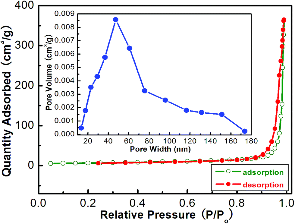 | ||
| Fig. 4 Typical N2 adsorption–desorption isotherms of flower-like In2O3. The inset is the corresponding pore size distribution curve. | ||
3.2. Gas-sensing properties for NO2
Gas sensing properties of the sensor using the In2O3 were investigated. It is well known that the response of a sensor is influenced by its operating temperature.27,28 In order to determine an optimum operating temperature, the response of the sensor towards 200 ppb NO2 was examined as a function of operating temperature. The correlations of the response and response time of the sensor based on the flower-like In2O3 nanostructures to 200 ppb NO2 with the operating temperature were measured and shown in Fig. 5. It revealed that the response time decreases with increasing operating temperature. This tendency indicates that fast response can be obtained through increasing the operating temperature. For the sensor using the flower-like In2O3 nanostructures, the response to 200 ppb NO2 slightly decreases when the operating temperatures varies from 80 °C to 140 °C. However, when the operating temperature is higher than 140 °C, the response sharply decreases. Accordingly, considering two aspects including the larger gas response and faster response speed of the sensor to 200 ppb NO2, the optimum operating temperature for the sensor using the as-obtained In2O3 is believed to be 140 °C, which is applied in all the investigations hereinafter. The response transients curve of the flower-like In2O3 nanostructures sensor to 200 ppb NO2 was measured at 140 °C (Fig. 6), and the response time and recovery time were about 100 s and 60 s, respectively. The six reversible cycles of the response transients curves indicated a stable and repeatable response characteristic, as shown in the inset of Fig. 6. It can be observed that the average response was ∼41.1 to 200 ppb NO2.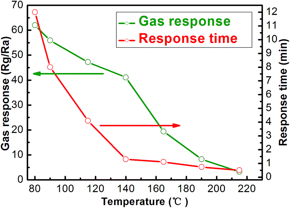 | ||
| Fig. 5 Correlations between the gas response and response time to 200 ppb NO2 with the operating temperature for the sensor using the as-obtained flower-like In2O3. | ||
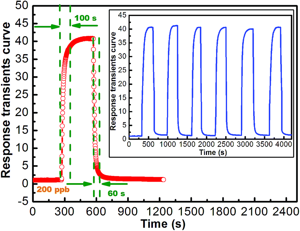 | ||
| Fig. 6 Response transients curve and the inset is the repeated response transients curves to 200 ppb for the sensor NO2 at 140 °C. | ||
The dynamic transient response curve of the sensors based on flower-like In2O3 nanostructures (Fig. 7) to different NO2 concentration were investigated at 140 °C. The resistance of the sensor increases upon exposure NO2, whereas it decreases upon the removal of NO2. Furthermore, the response of the sensor to NO2 increased with the increasing of the NO2 concentration. The gas response vs. concentration, as shown in the inset of Fig. 7. The flower-like In2O3 nanostructures sensor shows an acceptable response from the view of the practical application. A comparison between the sensing performances of the sensor and the literature reports17,29–33 is summarized in Table 1. From the table, it can be observed that the sensor based on the flower-like In2O3 nanostructures has a correspondingly higher gas response and lower working temperature. It manifests that the flower-like In2O3 nanostructures can enhance the sensing performance and as-synthesized samples might be useful to fabricate highly sensitive and low power consumption NO2 gas sensor device.
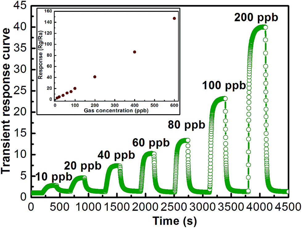 | ||
| Fig. 7 The dynamic transient response curve of the sensors and the gas responses to different concentrations of NO2 for the sensor using the flower-like In2O3 at 140 °C. | ||
| Sensing materials | NO2 concentration (ppm) | Working temperature (°C) | Sensor response | Reference |
|---|---|---|---|---|
| In2O3 nanofibers | 100 | 300 | 1.8 | 29 |
| In2O3 nanocrystals | 1 | 83 | ∼52.1 | 30 |
| In2O3 nanowires | 10 | 150 | ∼56 | 31 |
| WO3 thin films | 10 | 150 | 57 | 32 |
| WO3 nanosheets | 0.1 | 150 | ∼7 | 33 |
| In2O3 nanoplates | 1 | 150 | ∼73 | 17 |
| In2O3 flower-like | 0.2 | 140 | 41.1 | Present work |
Selectivity is an important parameter for gas sensor. Fig. 8 showed the cross-sensitivities of the sensor using the flower-like In2O3 nanostructures to various different gases, including O3, NH3, CO, H2S, SO2, Cl2, and C2H5OH. It is clear that the flower-like In2O3 sensor exhibits the largest response to NO2 relative to other gases. Such result indicates that the sensor using the In2O3 nanostructure exhibits an excellent selectivity to NO2 against the other tested gases at the working temperature of 140 °C.
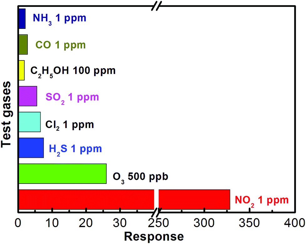 | ||
| Fig. 8 Cross-responses of the sensor to various test gases at 140 °C. | ||
For most semiconducting oxide type gas sensors, the change in resistance is primarily caused by the chemical adsorption and reaction of the gas molecules on the surface of the sensing materials. When In2O3 sensor is exposed to air, oxygen molecules adsorb on the surface of the materials to form O2−, O−, O2− ions by capturing electrons from the conduction band which results in increase in resistance. When the In2O3 is exposed to the atmosphere of NO2, it captures the electrons due to its higher electrophilic property which leads to the formation of adsorbed NO2(ads)−, and results in the further increase in resistance. However, desorption of NO2 can take place in several ways. The adsorbed NO2(ads)− reacts with adsorbed oxygen and gives following product.34–37
| NO2(gas) + e− → NO2(ads)− | (1) |
| NO2(gas) + O2(ads)− + 2e− → NO2(ads)− + 2O(ads)− | (2) |
The sharply decrease of the response at higher than 140 °C may be attributed to the decrease in number of active sites for the adsorption of NO2. Since at high temperature larger amount of oxygen molecules dissociate and adsorb on the active sites, the free active sites for the adsorption of NO2 molecules can be sharply reduced the response to NO2 becomes smaller. Another possibility may be that at such higher temperature the rate of adsorption is lower as compared to desorption. Accordingly, considering two aspects including the larger gas response and faster response speed of the sensor to NO2, the optimum operating temperature for the sensor using the as-obtained In2O3 is believed to be 140 °C. The efforts to enhance the gas response by decreasing the particle sizes down to a scale of several nanometres were counteracted by the formation of aggregates due to van der Waals attraction.38,39 This was the main reason for the low gas response in the aggregated nanoparticles. In contrast, the hierarchical structures provided well-defined and well-aligned micro-, and nano-porosity for effective gas diffusion.40 Therefore, a high gas response could be achieved using hierarchical nanostructures. In this work, the nanosheet-based In2O3 nanostructures offered abundant active sites for chemisorptions and reactions of NO2. As for the response and recovery characteristics, the flower-like In2O3 hierarchical nanostructures plays an important role in increasing the diffusion speed of NO2 and faster response and recovery speed can be expected. The more detailed reason and qualitative explanation need further investigation.
4. Conclusion
In summary, flower-like In2O3 had been successfully synthesized through a simple solution route combined with a subsequent calcining process. Field emission scanning electron microscopic and transmission electron microscopic results demonstrate that the flower-like hierarchical architectures were composed of porous nanosheets. In addition, the gas sensing properties of sensors based on as-synthesized In2O3 towards NO2 were investigated. The sensor fabricated from these hierarchical structures exhibits excellent NO2 sensing properties at relatively low operating temperature. The sensor response is about 2.7 to 10 ppb NO2 at 140 °C. These results suggest that our sensor might have potential application to fabricate highly sensitive and low power consumption NO2 gas sensor devices.Acknowledgements
This work is supported by the National Nature Science Foundation of China (no. 61134010, 61104203, 61327804, 61473132, 61304242 and 61474057), Application and Basic Research of Jilin Province (20130102010JC), The Henan Joint Funds of the National Natural Science Foundation of China (no. U1304612, U1404608, U1404216), Program for Chang Jiang Scholars and Innovative Research Team in University (no. IRT1017) and “863” High Technology Project (2013AA030902).References
- J. Y. Lao, J. Y. Huang, D. Z. Wang and Z. F. Ren, Nano Lett., 2003, 3, 235–238 CrossRef CAS.
- G. R. Li, C. Z. Yao, X. H. Lu, F. L. Zheng, Z. P. Feng, X. L. Yu, C. Y. Su and Y. X. Tong, Chem. Mater., 2008, 20, 3306–3314 CrossRef CAS.
- P. Sun, W. Zhao, Y. Cao, Y. Guan, Y. F. Sun and G. Y. Lu, CrystEngComm, 2011, 13, 3718–3724 RSC.
- J. Chen, L. N. Xu and W. Y. Li, Adv. Mater., 2005, 17, 582–586 CrossRef CAS.
- B. Sun, J. Horvat, H. S. Kim, W. S. Kim, J. Ahn and G. X. Wang, J. Phys. Chem. C, 2010, 114, 18753–18761 CAS.
- K. M. Li, Y. J. Li, M. Y. Lu, C. I. Kuo and L. J. Chen, Adv. Funct. Mater., 2009, 19, 2453–2456 CrossRef CAS.
- G. Korotcenkova, A. Cerneavschia, V. Brinzaria, A. Vasilieva, M. Ivanova, A. Cornetb, J. Moranteb, A. Cabotb and J. Arbiolb, Sens. Actuators, B, 2004, 99, 297–303 CrossRef PubMed.
- J. Tamaki, C. Naruo, Y. Yamamoto and M. Matsuoka, Sens. Actuators, B, 2002, 83, 190–194 CrossRef CAS.
- K. Obata, S. Kumazawa, K. Shimanoe, N. Miura and N. Yamazoe, Sens. Actuators, B, 2001, 76, 639–643 CrossRef CAS.
- T. Hyodo, H. Inoue, H. Motomur, K. Matsuo, T. Hashishin, J. Tamaki, Y. Shimizu and M. Egashira, Sens. Actuators, B, 2010, 151, 265–273 CrossRef CAS PubMed.
- D. H. Zhang, C. Li, S. Han, X. L. Liu, T. Tang, W. Jin and C. W. Zhou, Electronic transport studies of single-crystalline In2O3 nanowires, Appl. Phys. Lett., 2003, 82, 112–114 CrossRef CAS PubMed.
- C. G. Granqvist, Appl. Phys. A: Solids Surf., 1993, 57, 19–24 CrossRef.
- Y. Shigesato, S. Takaki and T. Haranoh, J. Appl. Phys., 1992, 71, 3356–3364 CrossRef CAS PubMed.
- A. Gurlo, M. Ivanovskaya, N. Bârsan, M. Schweizer-Berberich, U. Weimar, W. Göpel and A. Diéguez, Sens. Actuators, B, 1997, 44, 327–333 CrossRef.
- M. Liess, Thin Solid Films, 2002, 410, 183–187 CrossRef CAS.
- N. Singh, C. Y. Yan and P. S. Lee, Sens. Actuators, B, 2010, 150, 19–24 CrossRef CAS PubMed.
- X. M. Xu, D. W. Wang, W. B. Wang, B. Wang, P. Sun, Y. F. Sun and G. Y. Lu, RSC Adv., 2014, 4, 4831–4835 RSC.
- P. Guha, S. Kar and S. Chaudhuri, Appl. Phys. Lett., 2004, 85, 3851–3853 CrossRef CAS PubMed.
- Y. G. Yan, Y. Zhang, H. B. Zeng and L. D. Zhang, Cryst. Growth Des., 2007, 7, 940–943 CAS.
- P. C. Xu, Z. X. Cheng, Q. Y. Pan, J. Q. Xu, Q. Xiang, W. J. Yu and Y. L. Chu, Sens. Actuators, B, 2008, 130, 802–808 CrossRef CAS PubMed.
- C. H. Liang, G. W. Meng, Y. Lei, F. Phillipp and L. D. Zhang, Adv. Mater., 2001, 13, 1330–1333 CrossRef CAS.
- C. Li, D. H. Zhang, S. Han, X. L. Liu, T. Tang and C. W. Zhou, Adv. Mater., 2003, 15, 143–146 CrossRef CAS.
- Z. X. Cheng, X. B. Dong, Q. Y. Pan, J. C. Zhang and X. W. Dong, Mater. Lett., 2006, 60, 3137–3140 CrossRef CAS PubMed.
- X. P. Shen, H. J. Liu, X. Fan, Y. Jiang and J. M. Hong, J. Cryst. Growth, 2005, 276, 471–477 CrossRef CAS PubMed.
- Y. F. Hao, G. W. Meng, C. H. Ye and L. D. Zhang, Cryst. Growth Des., 2005, 5, 1617–1621 CAS.
- C. Q. Wang, D. Chen, X. L. Jiao and C. L. Chen, J. Phys. Chem. C, 2007, 111, 13398–13403 CAS.
- N. Yamazoe and K. Shimanoe, J. Electrochem. Soc., 2008, 155, 93–98 CrossRef PubMed.
- A. Kolmakov and M. Moskovits, Annu. Rev. Mater. Res., 2004, 34, 151–180 CrossRef CAS.
- W. Zheng, X. F. Lu, W. Wang, Z. Y. Li, H. N. Zhang, Y. Wang, Z. J. Wang and C. Wang, Sens. Actuators, B, 2009, 142, 61–65 CrossRef CAS PubMed.
- Ch. L. Chen, Y. L. Wei, D. R. Chen and X. L. Jiao, Mater. Chem. Phys., 2011, 125, 299–304 CrossRef CAS PubMed.
- C. S. Rout, K. Ganesh, A. Govindaraj and C. N. R. Rao, Appl. Phys. A, 2006, 85, 241–246 CrossRef CAS PubMed.
- Z. F. Liu, T. Yamazaki, Y. B. Shen, T. Kikuta and N. Nakatani, Sens. Actuators, B, 2007, 128, 173–178 CrossRef CAS PubMed.
- L. You, Y. F. Sun, J. Ma, Y. Guan, J. M. Sun, Y. Du and G. Y. Lu, Sens. Actuators, B, 2011, 157, 401–407 CrossRef CAS PubMed.
- N. Barsan, D. Koziej and U. Weimar, Sens. Actuators, B, 2007, 121, 18–35 CrossRef CAS PubMed.
- L. Francioso, A. Forleo, S. Capone, M. Epifani, A. M. Taurino and P. Siciliano, Sens. Actuators, B, 2006, 114, 646–655 CrossRef CAS PubMed.
- H. Steffes, C. Imawan, F. Solzbacher and E. Obermeier, in Proceedings of the International Conference Eurosensors XIII, The Hague, The Netherlands, 12–15 September, 1999, pp. 871–874 Search PubMed.
- M. Epifani, J. D. Prades, E. Comini, E. Pellicer, M. Avella, P. Siciliano, G. Faglia, A. Cirera, R. Scotti, F. Morazzoni and J. R. Morante, J. Phys. Chem. C, 2008, 112, 19540–19546 CAS.
- A. Gurlo, N. Bârsan, M. Ivanovskaya, U. Weimar and W. Göpel, Sens. Actuators, B, 1998, 47, 92–99 CrossRef CAS.
- G. Korotcenkov, V. Brinzari, A. Cerneavschi, M. Ivanov, V. Golovanov, A. Cornet, J. Morante, A. Cabot and J. Arbiol, Thin Solid Films, 2004, 460, 308–316 CrossRef PubMed.
- E. Li, Z. X. Cheng, J. Q. Xu, Q. Y. Pan, W. J. Yu and Y. L. Chu, Cryst. Growth Des., 2009, 9, 2146–2151 CAS.
| This journal is © The Royal Society of Chemistry 2015 |