
Si doped highly crystalline mesoporous In2O3 nanowires: synthesis, characterization and ultra-high response to NOx at room temperature†
Liyuan Yaoa,
Kan Kanac,
Yufei Lina,
Jiabao Songa,
Jingchao Wanga,
Jun Gaoa,
Peikang Shend,
Li Li*ab and
Keying Shi*a
aKey Laboratory of Functional Inorganic Material Chemistry, Ministry of Education, School of Chemistry and Materials Science, Heilongjiang University, Harbin, 150080, P. R. China. E-mail: shikeying2008@163.com; llwjjhlju@sina.cn; Fax: +86 4518667 3647; Tel: +86 451 8660 9141
bKey Laboratory of Chemical Engineering Process & Technology for High-efficiency Conversion, School of Chemistry and Materials Science, Heilongjiang University, Harbin, 150080, P. R. China
cInstitute of Advanced Technology, Heilongjiang Academy of Sciences, Harbin, 150000, P. R. China
dDepartment of Physics and Engineering, Sun Yat-sen University, Guangzhou, 510275, P. R. China
First published on 15th January 2015
Abstract
1D highly crystalline mesoporous In2O3 nanowires (INWs) coated by an amorphous silica (HCMIAS) ultrathin surface layer were successfully fabricated using SBA-16 as a hard template. Various techniques, including XRD, SEM, TEM and X-ray photoelectron spectroscopy (XPS), were employed for material characterization. All the results demonstrated that the obtained INW-2 sample, which contained 15 at% SiO2 and 85 at% In2O3 in 0.2 M In(NO3)3 solution, displayed high crystallinity with a rough surface coating layer of SiO2 in the atomic scale. The domain diameter of INW-2 was approximately 4–8 nm with the pore size of 3–5 nm. The NOx sensing properties of the INW-2 sensor exhibited an ultra-high response and selectivity with the low detection limit of 0.97 ppm and high response of 115.6 to 97.0 ppm NOx at RT. The excellent gas sensing property of the 1D morphology with amorphous silica was associated with its higher surface area and space-charge layer, which induced highly effective surface interactions between the target gas molecules and the surface active sites. Moreover, the synergetic and electronic effect on INW-2 favored the effective adsorption of NOx on the surface. All the factors considered had evident beneficial effects on enhancing the gas sensing performance of the sensor.
1 Introduction
As an important n-type semiconductor, the In2O3 porous structure has attracted particular attention to detect various gases1–4 such as oxidizing gases O3,5 O2,6 and NOx,7 as well as reducing gases for example NH3,8 CO or H2.9 In2O3 has been widely applied in thin-film-based sensing devices for decades. However, thin-film-based gas sensing devices possess critical limitations, such as relatively low maximum response, limited detection concentration, and higher operating temperatures (200–600 °C),10–12 and these bring substantial inconvenience for practical applications.As we know, gas sensing behavior is mainly depended on surface area, and surface-to-volume ratio of the materials significantly influences sensing performance.13,14 With ultra-high surface-to-volume ratios, 1D nanomaterials are believed to be able to deliver better performance than nanoparticles. Many efforts have been devoted to synthesize 1D In2O3 nanostructures, such as nanowires, nanobelts, and nanotubes, to meet the requirements of high performance chemical sensors.15–19 For example, Shen et al.2 synthesized high-aspect-ratio single-crystalline porous In2O3 nanobelts. The as-fabricated sensors can detect different chemicals (methanol, ethanol and acetone) down to the ppb level. Zou et al.20 synthesized Zn-doped flower-like In2O3 structures, which exhibited the highest response of 27.4 + 2.5 for 5 ppm NO2. The addition of a secondary component such as surface additives or dopants was a good method to synthesize these materials.21,22
Herein, we report 1D highly crystalline mesoporous In2O3 nanowires coated by amorphous silica (HCMIAS), which was fabricated with a rough surface in the atomic scale effectively using the inexpensive SiO2 as an additive, and the orderly mesoporous, SBA-16, as a template.23 The cross-linked In2O3 nanowires (INW) networks were obtained by structure replication with the amount of SiO2 incorporated into the In2O3 nanowires. The obtained materials were analysed by X-ray diffraction (XRD), transmission electron microscopy (TEM), Fourier transform infrared (FTIR) spectroscopy, X-ray photoelectron spectroscopy (XPS), electrochemical impedance spectroscopy (EIS) and Mott–Schottky (MS) plot measurements. The gas sensing properties were also investigated. The as-prepared INW-2 sensor fabricated by HCMIAS achieved super response and selectivity to NOx at room temperature (RT), which is expected for applications in automotive-exhaust gas sensors.
2 Experimental
2.1 Synthesis of highly crystalline mesoporous In2O3 nanowires
Mesoporous SBA-16 was synthesized as described in our previous work.24 HCMIAS controlled the growth of the mesoporous SBA-16 template. That is, SBA-16 was impregnated by the incipient wetness technique with different In(NO3)3 concentration solutions. During the impregnation process, a vacuum pump was used to reduce the air bound in the 3D SBA-16 in order to make sure that the In(NO3)3 solution could be impregnated completely. Then the samples were dried at ambient temperature, calcined in air to 550 °C, and maintained at that temperature for 4 h. The silica matrix was finally removed by leaching with a sodium hydroxide solution for 72 h. The obtained In2O3 NWs template with different In(NO3)3 concentrations of 0.1 M, 0.2 M, 0.3 M and 0.4 M In(NO3)3 were labeled as INW-1, INW-2, INW-3 and INW-4, respectively.2.2 Characterizations
The crystal phase of the samples was characterized by X-ray powder diffraction (XRD, D/max-IIIB-40 kV, Japan, Cu Kα radiation, λ = 1.5406 Å). The morphologies and structures of the In2O3 nanorods were observed by transmission electron microscopy (TEM, JEOL-2100, operated at 200 kV). The nitrogen adsorption–desorption isotherms were measured at 77 K using a Micromeritics Tristar II. The specific surface area of the materials was calculated using the Brunauer–Emmett–Teller (BET) method. Continuous wave photoluminescence spectra were obtained by a fluorescence spectrometer (LS55). Fourier transform infrared (FTIR) spectra were obtained with an FTIR spectrometer (Perkin Elmer Spectrum). X-Ray photoelectron spectra (XPS) were recorded with an AXIS ULPRA DLD (Shimadzu Corporation) system equipped to analyze the adsorbed oxygen species of samples. Electrochemical impedance spectroscopy (EIS) and Mott–Schottky (MS) plot measurements were carried out using an electrochemical working station (CHI660C, Shanghai, China) in a half-cell configuration at RT. In the EIS measurement, the range of frequency was 0.05 Hz to 100 kHz and the excitation amplitude was 5 mV.2.3 Gas sensing tests
99.6% alumina (7 mm × 5 mm × 0.38 mm) with two interdigitated Au electrodes on its top surface was used as the substrate. Each Au electrode contained 100 fingers, which interleaved with each other. The distance between the two fingers was 20 μm, and the Au electrodes on the Al2O3 substrates were cleaned by diluted HCl, distilled water and acetone. A certain amount of In2O3 NWs was dispersed in ethanol to form a suspension. The sensors were fabricated by a simple drop-casting method and dried at 70 °C for 5 h. The sensor was installed into a test chamber with an inlet and outlet. The electrical resistance measurements of the sensor were carried out at RT and relative humidity (RH) around 42%. The NOx gas concentration was controlled by injecting a certain amount of gas and the chamber was purged with air to recover the sensor resistance. The gas response was defined as the ratio (Rg − Ra)/Ra, where Ra and Rg were the resistances measured in air and the test at gas atmosphere, respectively. The applied voltage was 5 V. We used a pump to replace the air in the chamber. The sensing device is shown in Fig. S6.† The response of the synthesized INW-2 sensor to NOx gases was detected in the RH range of 42–80% at room temperature.3 Results and discussion
3.1 Composition and morphology
The XRD patterns of HCMIAS are shown in Fig. 1A. The diffraction peaks of the In2O3 NWs around 21.60°, 30.66°, 35.54°, 45.77°, 51.01° and 60.66° correspond to the (211), (222), (400), (134), (440) and (622) planes with the d spacing of 4.13 Å, 2.92 Å, 2.53 Å, 1.98 Å, 1.79 Å and 1.53 Å, respectively. This indicates the formation of a highly crystalline cubic structure (JCPDS card no. 89-4595). As shown in Fig. 1A, the samples displayed a broader full width at the half of the In2O3 peaks when the In(NO3)3 solution decreased from INW-4 to INW-1. The crystallinity of the In2O3 nanowires increased in line with the In(NO3)3 solution concentration. In addition, no evident characteristic peaks (such as SiO2) were present in the samples. | ||
| Fig. 1 (A) XRD diffraction patterns of the mesoporous In2O3 nanowires (a) INW-1; (b) INW-2; (c) INW-3; (d) INW-4. (B) Nitrogen adsorption–desorption isotherms of (a) INW-1; (b) INW-2; (c) INW-3; (d) INW-4, and the insert shows the pore-size distribution curves of the four samples. | ||
The N2 adsorption–desorption results are displayed in Fig. 1B. It indicates that all of the HCMIAS exhibited type IV isotherms. The pore size distributions of the HCMIAS are shown in the inset of Fig. 1B. For INW-1, INW-2, INW-3 and INW-4, the BET specific surface were 37.45 m2 g−1, 57.23 m2 g−1, 19.84 m2 g−1 and 14.74 m2 g−1, respectively. Among them, the INW-2 sample had the highest specific surface area. The pore size was mostly concentrated at 3.64 nm and 33.8 nm. For the other samples, the pore size was in the range of 10–80 nm. Generally, the pore size distribution was attributed to the interspaces of the nanowires and mesoporous. This was beneficial for the process of gas adsorption on the material surface in this case. The BET specific surface areas of the In2O3 samples were substantially lower than that of the SBA-16 template (as shown in Fig. S1†).
TEM images of the HCMIAS mesoporous structure are shown in Fig. 2, in which we could see that HCMIAS have a regular fibre like morphology with a uniform diameter of 4–8 nm. This was due to the confined growth of the material in the channels of SBA-16 template. The average mesoporous size on the surface of the nanowires was 3–5 nm, which contained the cross-linked In2O3 nanowires networks. That is, the HCMIAS were connected with each other to build the hierarchical architectures. The connectivities of the HCMIAS might provide the channels of electron transmission for gas absorption.
 | ||
| Fig. 2 TEM images of the mesoporous highly crystalline In2O3 NWs doped by amorphous silica (a) and (a1) INW-1; (b) and (b1) INW-2, the inset of (b1) is the size distribution of INW-2; (c) and (c1) INW-3 and (d) and (d1) INW-4. | ||
The high-resolution TEM (HRTEM) images (Fig. 2a1–d1) of HCMIAS were further confirmed to be highly crystalline. The interplanar spacing of the In2O3 nanowires measured 5.06 Å, 4.13 Å, 2.92 Å and 2.52 Å, which correspond to the d spacing of the (200), (211), (222), and (400) planes in cubic In2O3. Fig. 2b and b1 display the detailed information of the INW-2 sample. There were many mesopores on the surface of the INW-2 nanowires in the HRTEM images.
Fig. 2d and d1 indicate that the sample of INW-4 was a mixture of mesoporous In2O3 nanoparticles and nanowires. The sizes of some mesoporous In2O3 nanoparticles changed from 20 to 100 nm. The excess In(NO3)3 covered the SBA-16 template, and this made it difficult to form nanowires when SBA-16 was dissolved by sodium hydroxide solution. Thus, it could be found that the INW-1, INW-2 and INW-3 samples are irregularly distributed in wire-like structures. They are highly crystalline mesoporous nanowires (particularly INW-1 and INW-2). Fig. 2 and S2† further reveal that the In2O3 nanowires were well-crystallized with a narrow size distribution of 4–8 nm.
STEM image and EDS mapping of INW-2 are displayed in Fig. 3. Fig. 3a and e are bright field images of INW-2. Fig. 3b–d revealed the existence of O, In and Si elements accordingly. It is clearly observed that the distribution of these elements is uniform. Fig. 3f shows an EDS line scan across four nanowires lying ∼22 nm from the INW-2 interface with the associated STEM image (Fig. 3e and S2f†). The EDS line scan reveals the presence of In2O3 and SiO2. The dashed line in the Fig. 3f indicates that the position of the interface is between the In2O3 and SiO2. Small isolated SiO2 on In2O3 NWs boundaries were away from the In2O3 interface. They are believed to form core–shell like In2O3 NWs after they were doped by little amount of SiO2.
 | ||
| Fig. 3 STEM image/EDS mapping of the INW-2 (a) bright field image; (b), (c) and (d) corresponding to O, In and Si elemental mapping, respectively; (e) STEM image of INW-2 and (f) EDS of the INW-2 alonged with the line scan analysis (the scanning direction is shown as the red arrow). | ||
Furthermore, the photoluminescence (PL) emission with 325 nm excitation and UV-vis absorption of the samples were studied at RT. Fig. 4a shows very strong violet emission bands in the range of 385–415 nm. The maximum intensity centered at 400 nm could be attributed to the oxygen vacancies of pure In2O3 NWs. This result was similar to In2O3 nanofibers with PL emission peaks at 378–420 nm.25 The PL depended on the disorder of the system. The disorder in amorphous silica could lead to a broad peak (Fig. S3A†).
 | ||
| Fig. 4 Curve fitting results in the PL spectra of samples with 325 nm excitation at RT (a) In2O3, (b) INW-1, (c) INW-2, and (d) INW-4. | ||
As shown in Fig. 4b–d, the emissions presented in 399 or 400 nm (maximum) were attributed to the oxygen vacancies defects in In2O3.24 The emission at 431 nm (428 or 439 nm) corresponds to intrinsic diamagnetic centers (O–Si–O, violet emission). The emission at 460 or 466 nm is attributed to oxygen-related defect sites or (![[triple bond, length as m-dash]](https://www.rsc.org/images/entities/char_e002.gif) Si–O˙),26 and the 507 nm emission belongs to Si+ ion implantation.27 This was confirmed by the XPS analysis (Fig. 6). It could be seen that, O–Si–O at the 428 (or 431) nm (violet emission) increased from pure In2O3, INW-4, INW-1 to INW-2. For INW-2, the abrupt increase of the PL intensity around 428 nm indicated that the oxygen deficiency emissions were enhanced when a thin-layer of SiO2 was coated on the surface of In2O3 NWs. This might be related to the amount of SiO2 in the samples. In addition, HCMIAS with a high ratio and peculiar morphologies could be in favor of the existence of oxygen vacancies. A large quantity of oxygen vacancies would induce the formation of new energy levels in the band gap.28
Si–O˙),26 and the 507 nm emission belongs to Si+ ion implantation.27 This was confirmed by the XPS analysis (Fig. 6). It could be seen that, O–Si–O at the 428 (or 431) nm (violet emission) increased from pure In2O3, INW-4, INW-1 to INW-2. For INW-2, the abrupt increase of the PL intensity around 428 nm indicated that the oxygen deficiency emissions were enhanced when a thin-layer of SiO2 was coated on the surface of In2O3 NWs. This might be related to the amount of SiO2 in the samples. In addition, HCMIAS with a high ratio and peculiar morphologies could be in favor of the existence of oxygen vacancies. A large quantity of oxygen vacancies would induce the formation of new energy levels in the band gap.28
As illustrated in Fig. S3B,† the strong UV absorption of In2O3 which occurs at 300–310 nm could be attributed to the electronic transition from the valence band to the conduction band.29 Moreover, a strong UV absorption of In2O3 NWs occurred at 300–310 nm, which indicated the existence of a weak quantum confinement effect30 as the obtained In2O3 NWs diameters concentrated at 4–8 nm (the critical Bohr radius of In2O3 is about 2.14 nm).27
Fig. 5 shows the TEM/HRTEM images of INW-2. The easily found defects are shown in Fig. 5a–e at the irregular edges of a single In2O3 NW, and the narrowest width of the In2O3 NWs is about 4 nm (Fig. 5c and S2†). The contrast of the HRTEM images displaying the mesopores of the crystal In2O3 NWs are shown in Fig. 5a and f. The size of mesopores was about 3–5 nm. Fig. 5b–f show the defects at the branching locations. The red arrows point out the linear and planar defects, which might be formed by the oxygen vacancies. The irregular edges and pores that exist on the crystal In2O3 NWs might enlarge the specific surface area (Fig. 1B) and increase the surface defects.
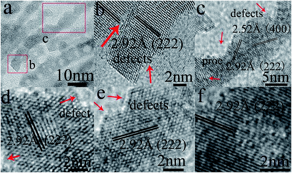 | ||
| Fig. 5 TEM/HRTEM images of the INW-2, (a) low magnification TEM image of INW-2; (b–e) HRTEM images of the highly crystal In2O3 NWs of INW-2; (f) pores in INW-2. | ||
In this work, the HCMIAS were synthesized by the hard template, SBA-16. When SiO2 was dissolved by sodium hydroxide solution at a different time, the obtained In2O3 NWs surface might be firmly coated by an ultrathin layer of amorphous silica (Fig. 3f). The amorphous edges were observed on the surface of some In2O3 NWs (Fig. 2a1 and b1). Fig. 2 shows that the homogeneous coverage occurred between the amorphous silica and In2O3. However, in Fig. 2 and particularly in Fig. 5, there are only crystal lattices defects on the sides and mesopores of the In2O3 NWs, and no evident shell–core structure was observed between the mesoporous crystalline In2O3 NWs and amorphous silica. Therefore, it was deduced that the average thickness of the SiO2 coating layer might be less than 1 nm. The obtained In2O3 NWs was highly crystalline with a rough surface coating layer of SiO2 in the atomic scale.
XPS is an effective surface test technique for characterizing elemental composition and chemical states. The electron density of an element influences its binding energy. An increase in binding energy could imply the lowering of the electron density. To explore the effect of Si additives in the In2O3 NWs, the XPS spectra of O 1s are displayed in Fig. 6 and S4A.† The O 1s peaks of INW-1, INW-2, INW-3 and INW-4 were fitted by Gaussian simulation peaks. The peak located at 529.3 ± 0.2 eV, which was marked as Oa, could be attributed to the oxide lattice (O2− ions) in In2O3. The peak named Ob at 530.9 eV corresponds to the oxygen deficiencies, which are called oxygen vacancies. The peak at 532.2 eV, named Oc, is usually assigned to the loosely bound oxygen in amorphous SiO2 or the partial weakly adsorbed oxygen species of O2−.31
 | ||
| Fig. 6 XPS spectra of O 1s (A) INW-1, (B) INW-2, (C) INW-3, (D) INW-4; and (E) Si 2p; (F) In 3d. | ||
XPS results of Fig. 6 further confirmed the abovementioned speculation and revealed the existing In, O and Si elements in all of the samples. According to the results, the calculated oxygen vacancy defect (Ob peak area) of INW-1, INW-2, INW-3 and INW-4 are about 33.2%, 47.2%, 43.76% and 29.9%, respectively. The calculated chemisorbed oxygen (Oc) is 32.4%, 33.2%, 19.2% and 31.8%. Therefore, the peak area of oxygen vacancy defects and the chemisorbed oxygen of INW-2 were the biggest among the four samples. Because the oxygen vacancy defects were taken as shallow donors,32 more donors would exist as more oxygen vacancies became available. Moreover, chemisorbed oxygen was suggested to act as an electron donor, and could be defined as an n-type semiconductor.33 Oxygen vacancies and chemisorbed oxygen are known for their excellent catalytic activity in gas sensors, and they improved the performance of NOx sensors.
In the region of Si 2p (Fig. 6E), the peak of pure SiO2 (SBA-16) at 103.7 eV was assigned to Si4+ (Si–O).34 However, for the INW-1, INW-2 and INW-4 samples, the binding energy decreased to 102 (or 101.4) eV, which was assigned to In–O–Si.35 This indicated that the electrons on the Si atoms had increased compared with pure SiO2. The values of Si contents were roughly 7.78 at%, 14.2 at%, and 9.3 at% for INW-1, INW-2 and INW-4, respectively. This further indicated that the electrons on the Si atoms had increased in comparison with pure SiO2. A little peak at 104.1 eV existed in all three samples. This demonstrated the existence of the SiOx phase (x = 1.94).36 When the ratio of O![[thin space (1/6-em)]](https://www.rsc.org/images/entities/char_2009.gif) :Si was lower than 2.0, oxygen vacancies existed, where such oxygen vacancies would give rise to the formation of a defect level. The defect level would then act as hole-traps, and thus promote charge transfer.37
:Si was lower than 2.0, oxygen vacancies existed, where such oxygen vacancies would give rise to the formation of a defect level. The defect level would then act as hole-traps, and thus promote charge transfer.37
In the region of In 3d (Fig. 6F), the binding energy of pure In2O3 was 443.8 eV (In–O–In). Nevertheless, for the INW-1, INW-2 and INW-4 samples, the binding energy increased to 443.9 eV, 444 eV and 444.1 eV correspondingly. This indicated that the electron densities on the In atoms had decreased compared with pure In2O3. Similarly with the In 4d (Fig. S4B†), there were also subtle changes in the In 4d peak shape and a shift to a high binding energy after it was doped by SiO2. In this region, the position of the In 4d peak displayed a chemical shift of about 0.1 or 0.2 eV from the peak of pure In2O3. This was possibly attributed to the formation of the In–O–Si bond.34 Due to the higher electronegativity of oxygen, the electrons could be transferred from In and Si to O, and Si could supply less electrons than In in the In–O–Si bond. Consequently, in comparison with the In–O–In bond, more electrons would be transferred from In to O in the In–O–Si bond. This would result in the decrease of the electron densities on the In atoms. FT-IR results (Fig. 5S†) also confirmed the existence of the In–O–Si bond.
In general, the resistance of materials in air played an important role in their gas responses. The change of the carrier concentration was caused by the adsorption of the target gas molecules onto the surfaces of the semiconductor. The better electron transportation in air may induce a faster response. Therefore, in order to further verify the electron densities of the HCMIAS, MS curves were investigated.
As illustrated in Fig. 7a, the MS curves of the INW-1 and INW-2 samples were approximately linear. The two samples exhibited a positive slope in the MS plots and the linear slope changed from 0.45 to 0.7 V, which was consistent with the shape of an n-type semiconductor.
 | ||
| Fig. 7 (a) Mott–Schottky plots of the INW-1, INW-2 and INW-4 electrodes in 0.05 M H2SO4 electrolyte were measured at a frequency of 1000 Hz; (b) Nyquist plots of different samples and equivalent circuit model (the upper left inset) of INW-1, INW-2 and INW-4 were measured in the frequency range from 0.05 Hz to 100 kHz with 0.4 V; the bottom left inset shows the Nyquist plots of INW-2 and the logarithmic plot of the imaginary part of the impedance. | ||
Moreover, the slope of the MS curves could calculate the carrier concentration using (eqn (1)) as follows.
| Nd = (2/e0εε0)[d(1/C2)/dV]−1 | (1) |
Generally, particle size effects could positively influence the catalytic activity and sensing performance. The sensing performance was in particularly related to the Debye length, which could be calculated from eqn (2):
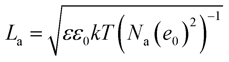 | (2) |
In addition, EIS measurements were carried out and the results are shown in Fig. 7b. The Nyquist plots of the INW-1, INW-2 and INW-4 electrodes were almost identical. The Nyquist plots were fitted by an appropriate electric equivalent circuit (the upper left inset in Fig. 7b) and the obtained impedance parameters are given in Table 1. Here, the RΩ indicated the uncompensated bulk resistance of the electrolyte, separator and electrode; the (Q1R1) parallel element corresponds to the electrode film interface capacitance (Q1) and surface pore resistance (R1);39 the (Q2R2) parallel element might attribute to the possible breakdown of the electrolyte and electrode material internal microstructures; Rct is attributed to the charge-transfer resistance at the active material interface; C is the constant phase angle element, involving double layer capacitance.
| Samples | RΩ (Ω) | R1 (Ω) | R2 (Ω) | Rct (Ω) | Na (cm−3) |
|---|---|---|---|---|---|
| INW-1 | 252 | 9.64 × 10⁴ | 2592 | 1563 | 1.34 × 10¹⁸ |
| INW-2 | 100 | 1215 | 3.38 × 10⁴ | 1332 | 2.03 × 10¹⁸ |
| INW-4 | 6314 | 635.8 | 2.53 × 10⁴ | 9.09 × 10⁴ | 6.15 × 10¹⁸ |
Furthermore, the values of INW-2 resistance, RΩ, and charge-transfer resistance, Rct, were lower than that of INW-1 and INW-4, respectively. Both RΩ and Rct were related to the conductivity of the electrode. Thus, it could be confirmed that INW-2 modified electrode exhibited considerably higher conductivity and improved the electron transportation. Furthermore, the slope of the logarithmic plot of the ImZ (the imaginary part of the INW-2 impedance) and ω (angular frequency) was −0.49, and the approach −1/2 (−0.49) indicated a porous structure in the INW-2 electrode.40
3.2 Sensor performance
The gas response results for 97–0.97 ppm NOx of HCMIAS were investigated at RT in air (humidity 42%) (as shown in Fig. 8 and Table S1†). Fig. 8 also depicts the representative dynamic gas response of the HCMIAS gas sensor for different concentrations of NOx at RT. | ||
| Fig. 8 The results of the gas response of the HCMIAs synthesized by In(NO3)3 sensors to 97–0.97 ppm NOx at RT in air (humidity 42%) (A) the representative response–recovery cyclic curves of INW-2; (B) the gas sensitivities of the samples INW-1, INW-2, INW-3 and INW-4; (C) the response time curves of INW-1, INW-2, INW-3 and INW-4; (D) the dynamic response of different In2O3 samples: (a) INW-1, (b) INW-2, (c) INW-3 and (d) INW-4 corresponding to 97 ppm NOx at RT. The inset is the response of INW-3 and INW-4 to 97 ppm NOx; (E) the response of INW-3 compared with INW-2 to 97 ppm NOx; (F) bar chart shows the response value of the INW-2 sensor for four different gases. | ||
Fig. 8A shows the gas response results of the typical sample INW-2 sensor during cyclic exposure to NOx. When NOx gas was injected into the sensing chamber from 97 to 0.97 ppm at RT, the resistance of the INW-2 sensor rose rapidly and reached a maximum resistance value in a shorter time. Apparently, the thin-film sensor based on INW-2 exhibited rapid and reversible response signals to NOx gas even at the lowest exposure level (0.97 ppm) both in the adsorption and desorption process. When the concentration of NOx was 97 ppm, the response time was 118 s, whereas the highest response could reach 115.6. This was considerably higher than others at RT (shown in Table S3†). In most cases, the response of the HCMIAS sensor declined as the response time increased. However, when NOx was 0.97 ppm, the response was only 1.68, and the response time was 194.7 s, which was faster than the response time of NOx with a concentration at 4.85 (or 2.91) ppm. This was associated with the gas concentration, gas diffusion and absorbance on the surface of the nanowires. It should be noted that the INW-2 sensor exhibited the lowest detection limit of 0.97 ppm at RT.
The bar graphs of the four In2O3 NWs sensors to NOx at RT in air are shown in Fig. 8B. Fig. 8C shows the response time of the samples at RT. It could be seen that only the INW-2 sensor could reach the lowest detectable concentration, and have the highest responsiveness and fast responsive time in the whole range of NOx concentrations. Fig. 8B and C show the typical response curves of the four In2O3 NWs sensors to NOx (97–0.97 ppm) at RT. The responses of the four sensors to 97 ppm NOx were 39.5, 115, 17.4, and 1.43. Compared with INW-1, INW-3 and INW-4, the INW-2 sensor showed the highest responsiveness to 97 ppm NOx, and the response of the INW-2 sensor was 2.91, 6.64, and 80.4 times higher than INW-1, INW-3 and INW-4 correspondingly. INW-3 sensor had the fastest shortest response time to NOx (Table. S1†).
Table S1† lists the gas response of each sample in the concentration of NOx ranging from 97 to 0.97 ppm. The resistance of all samples underwent a drastic increase upon the injection of NOx and a decline to its initial value after the sensor was exposed to air for a period of time. The response of the different sensors changed with the changing NOx gas concentration. These all show that the four HCMIAS sensors displayed the behavior of n-type semiconductors. In comparison with INW-1, INW-3 and INW-4 (Fig. 8B, C and Table. S1†), the INW-2 gas sensor showed high gas sensing response behavior at RT, and the lowest detection limit for 0.97 ppm NOx. The maximum response to 97 ppm NOx was 115.6. Simultaneously, it was also higher than the meso-20 AI NTs sensor to 97 ppm NOx of 100, as described in our previous work.41
In this work, the response time of the sensor is defined as the required time to reach 85% of the maximum sensor resistance in the case of target gas. Compared with the INW-3 sensor, the change amplitude of the INW-2 sensor resistance was equal to the INW-3 sensor for 97 ppm NOx at RT. As shown in Fig. 8E, when the response was 17.4, the required time of INW-2 was about 17 s, which was faster than that of INW-3 i.e. about 18 s. The abovementioned results indicated that the INW-2 sensor had a better sensing performance than the others.
In order to further study the gas sensing properties of the In2O3 NWs sensor, the selectivity of the INW-2 sensor was tested at different concentrations of various gases such as NOx, NH3, CO and H2S. The results are displayed in Fig. 8F. The INW-2 sensor showed the highest response to NOx with a value of up to 115.6 for 97 ppm at RT. For 970 ppm NH3 gas, the response was not higher than 0.8, whereas the response was 0.01 for 48500 ppm CO. The results also indicated that the In2O3 NWs sensor had no response to H2S. Therefore, it might be concluded that the INW-2 sensor showed evident selectivity. It also had the highest gas response to NOx, indicating that it would be an excellent NOx sensor for automotive-gas detection.
It is well known that humidity is one of the significant factors in the gas sensing process, in which the degree of humidity influences the sensing performance of oxide semiconductors. In order to verify the influence of humidity on the response of the INW-2 sensor to NOx, we recorded the response of the INW-2 sensor in the RH range of 42–80% to 97–0.97 ppm NOx at RT in air. Detailed results of the gas response are shown in Fig. S7 and Table S2.† It could be seen that the response of the sensor to NOx gases slightly decreased as the RH increased. The humidity has little effect on the NOx gas sensing response in our experience.
3.3 Discussion of sensing mechanism
The response in a gas sensor is a complex phenomenon, which is determined by factors such as (I) the surface reactions/adsorption processes; (II) the resulting charge transfer processes with the underlying semiconducting material, and the transportation of charge carriers within the sensing layer. Considering the abovementioned factors, the discussion on the sensing mechanism could be summarized as follows:(I) The synergetic effect on the gas sensing characteristic between the 1D mesoporous crystalline In2O3 NWs and amorphous silica, including chemical interaction between SiO2 and In2O3 at the interfaces and gas sensing reaction.
The cross-linked In2O3 NWs networks which were formed by structure replication of SBA-16 in the INW-2 sensor were connected with each other to build hierarchical pores (Fig. 2 and 3). Moreover, the single INW-2 possessed the unique transportation of charge carriers with the sensing layer and interface structure Si–O–In bonds being formed42 (Fig. 6F, S5† and 9b).26 INW-2 with an ultrathin coating layer of SiO2 in the atomic scale had high crystal quality nanostructures. In addition, the amorphous silica was dispersed on the surface of the In2O3 NWs uniformly as shown in Fig. 3. The electron density of the O–Si side was higher than that of the In atoms in the In–O–Si bond (Fig. 6 and S4†). These were all beneficial to the sensing performance of the oxidizing gases, NOx. On one hand, the large amount of mesopores of 3.64 and 33.8 nm in size, which existed in the INW-2 nanowires, was advantageous for gas adsorption–desorption and diffusion. The construction of electron conduction paths through the connected crystal mesoporous In2O3 NWs became easier. Abundant hydroxyls and chemisorbed oxygen on the surface of the amorphous silica caused more extended surface interactions with gas molecules.
 | ||
| Fig. 9 Structural and band models of the conductive mechanism of the INW-2 sensor exposed to air and NOx (a) the INW-2 NW; (b) the interface model of In2O3–SiO2 in INW-2; (c) the illustration of the space-charge layer distribution on INW-2 (including regions 1 and 2); (d) HRTEM images showing defects at the branching locations. | ||
Most importantly, the response of the sensor may depend on its Debye length (La). As calculated above, the La of the In2O3 NWs (INW-2) was approximately 2.5 nm. Here, the single INW-2 NWs could be divided into two regions: 1 and 2 (Fig. 9c). First, region 1 corresponds to the INW-2 NWs, which contained 3 nm pores. The width of the left or/and right pore was about 2.5 nm, which was close to the La of 2.5 nm. In this case, the space-charge layer had an effect on the electron density in the nanowires only, and could be regarded as fully depleted cylinders. The fully depleted cylinders occurred when the Fermi level was totally controlled by surface states under nearly flat energy bands if the potential barrier was neglected.43 Second, region 2 corresponds to the INW-2 NWs without pores. The domain diameter of the single nanowires was 5–7 nm, which is between 2La and 3La (Fig. 2). And the depletion layer had an effect on both the electron density and potential barrier in the nanowires. Thus, the surface depletion layer and potential barrier were used to control the sensor resistance. As shown in Fig. 1b, 2b and S2a,† there were a lot of mesopores of 3–5 nm on INW-2. Hence, region 1 without a potential barrier in the INW-2 sensor was abundant. Therefore, the INW-2 sensor exhibited an ultrahigh response performance to NOx ranging from 97 to 0.97 ppm.
(II) Electronic effect on gas sensing performance, which involved electronic interactions between In2O3 and the SiO2 additive (electron density variation), electronic transmission in the cross-linked In2O3 NWs networks, and the effects of chemisorbed oxygen (O2−) and oxygen vacancies (defects).
As well known, the In2O3 nanowires doped by SiO2 core–shell like structure could be classified as a semiconductor heterostructure. Both the conduction and the valence band edges of the narrow bandgap core of In2O3 were located within the energy gap of the wide-band gap shell semiconductor (SiO2). Consequently, the electron–hole (e–h) pair exited near the interface tended to localize in the core semiconductor.44
The suitable resistance and better electron transportation (high carrier density) of the INW-2 NWs exhibited higher conductivity and carrier density (Fig. 8D and Table 1). The abundant crystal oxygen defects and chemisorbed oxygen (Fig. 4–6) of the In2O3 NWs doped by SiO2 with irregular edges and pores could also favour the existence of large quantities of oxygen vacancies. This structure did not only provide highly energetic sites to further enhance the interaction between NOx molecules and the metal oxide, but also induced the formation of new energy levels in the band gap, which served as donors. Furthermore, INW-2 contained chemisorbed oxygen, which is suggested to act as an electron donor. This demonstrated that the addition of 14.2 at% SiO2 additive to the In2O3 NWs (INW-2) could increase both the donors and impurity bands. These would hence benefit the electron transmission to the absorption gas (such as O2 and NOx), which enhanced the performance of the NOx sensors and they exhibited excellent response characteristics.
Fig. 9a displays the conductive mechanism of the INW-2 NWs and presents the bonding configuration models of In2O3–SiO2 at the interfaces. The electronic transportation and the NOx gas response in INW-2 are described as follows:
When the sensor was exposed to air, oxygen molecules could easily trap the electrons from the conductance band of In2O3 to form chemisorbed oxygen (O2−) (reaction 1 (R1)). Then, NOx gas was injected to the INW-2 sensor. The target gas molecules, NOx, were directly adsorbed onto INW-2 because of the high electron affinity of the NOx molecules. This made electrons transfer easily from the INW-2 sensor to the surface NOx adsorbates and led to a decrease in electron density. As a result, the resistance of the INW-2 sensor increased. The response time of the gas sensor was extremely sensitive to electron density and electron diffusion/transportation. The adsorption of NOx on INW-2 led to the formation of NOx− (R2).
In addition, the adsorbed NO2 reacted with O2−/O− and later generated bidentate NO3− (s) and NO2− (R3).45
| O2 + e− ↔ O2−(2O−) | (R1) |
| NOx + e → NOx− | (R2) |
| NOx + O2− + 2e → NOx+1− + O− | (R3) |
For reducing gases such as CO, in open air, the formation of oxygen adsorbates (O2− or O−) on the surface of In2O3 resulted in an electron-depleted surface layer due to electron transfer from In2O3 to oxygen. The reduction process resulted in an increase in film conductivity, and the reoxidation process contributed to a decrease in this parameter. Thus, in such approach, film conductivity is determined by the concentration of the charge carrier which changed its valence state, and chemisorption is only an intermediate step in these chemical reactions. The mechanism of CO gas sensing was based on the (R4) and (R5):46
| 2CO + O2− → 2CO2 + e− | (R4) |
| CO + O− → CO2 + e− | (R5) |
4 Conclusions
HCMIAS with sizes of 4–8 nm and pore sizes of 3–5 nm were synthesized by the hard template, SBA-16. INW-2 was obtained from a 0.2 M In(NO3)3 solution and exhibited the smallest diameter, the largest specific surface area and abundant mesopores. INW-2 contained 15 at% SiO2 and 85 at% In2O3, which were crystalline with a rough surface coating layer of SiO2 in the atomic scale, featuring a high density of defects. This special structure provided a greater number of available active centers for gas/surface reactions. The INW-2 sensor possessed an ultrahigh response and selectivity to NOx with the low detection limit of 0.97 ppm and high response of 115.6 to 97.0 ppm NOx at RT. The HCMIAS served as an excellent sensitive material, allowing for further enhancement in gas adsorption–desorption and chemical/electronic synergistic effects. The as-obtained HCMIAS is promising for applications in gas sensors, optical and electric devices because of the novel shape of their building blocks and controllable thickness (of the surface layer SiO2).Acknowledgements
This work was supported by the Union Funds of the National Natural Science Foundation of China (no. U1034003), the Key Projects of the Natural Science Foundation of Heilongjiang Province (no. B201105), and the Special Funds for Investment of Sci-tech Innovation of Harbin (2012RFXXG102).References
- X. L. Hu, X. Zhou, B. Wang, P. Sun, X. W. Li, C. Wang, J. Y. Liu and G. Y. Lu, RSC Adv., 2015, 5, 4609 RSC.
- Y. S. Li, J. F. Chao, D. Chen, S. X. Ouyang, J. H. Ye and G. Z. Shen, J. Mater. Chem., 2011, 21, 12852 RSC.
- L. P. Gao, Z. X. Cheng, Q. Xiang, Y. Zhang and J. Q. Xu, Sens. Actuators, B, 2015, 208, 436 CrossRef CAS PubMed.
- B. J. Kim, I. G. Song and J. S. Kim, Electron. Mater. Lett., 2014, 2, 509 CrossRef.
- G. Korotcenkov, A. Cerneavschi, V. Brinzari, A. Vasiliev, M. Ivanov, A. Cornet, J. Morante, A. Cabot and J. Arbiol, Sens. Actuators, B, 2004, 99, 297 CrossRef CAS PubMed.
- G. Neri, A. Bonavita, G. Micali, G. Rizzo, N. Pinna and M. Niederberger, Sens. Actuators, B, 2007, 127, 455 CrossRef CAS PubMed.
- M. Ali, C. Y. Wang, C. C. Röhlig, V. Cimalla, T. Stauden and O. Ambacher, Sens. Actuators, B, 2008, 129, 467 CrossRef CAS PubMed.
- S. Cui, H. Pu, G. Lu, Z. Wen, E. C. Mattson, C. Hirschmugl, M. Gajdardziska-Josifovska, M. Weinert and J. Chen, ACS Appl. Mater. Interfaces, 2012, 4, 4898 CAS.
- G. Korotcenkov, V. Brinzari, A. Cerneavschi, M. Ivanov, A. Cornet, J. Morante, A. Cabot and J. Arbiol, Sens. Actuators, B, 2004, 98, 122 CrossRef CAS PubMed.
- L. G. Bloor, J. Manzi, R. Binions, I. P. Parkin, D. Pugh, A. Afonja, C. S. Blackman, S. Sathasivam and C. J. Carmalt, Chem. Mater., 2012, 24, 2864 CrossRef CAS.
- S. Kannan, L. Rieth and F. Solzbacher, Sens. Actuators, B, 2010, 149, 8 CrossRef CAS PubMed.
- N. Singh, A. Ponzoni, E. Comini and P. S. Lee, Sens. Actuators, B, 2012, 171, 244 CrossRef PubMed.
- M. Mashock, K. Yu, S. Cui, S. Mao, G. Lu and J. Chen, ACS Appl. Mater. Interfaces, 2012, 4, 4192 CAS.
- M. Arafat, B. Dinan, S. A. Akbar and A. Haseeb, Sensors, 2012, 12, 7207 CrossRef CAS PubMed.
- C. Y. Ma, Z. Mu, J. J. Li, Y. G. Jin, J. Cheng, G. Q. Lu, Z. P. Hao and S. Z. Qiao, J. Am. Chem. Soc., 2010, 132, 2608 CrossRef CAS PubMed.
- J. M. Kisler, A. Dähler, G. W. Stevens and A. J. O'Connor, Microporous Mesoporous Mater., 2001, 44, 769 CrossRef.
- X. He and D. Antonelli, Angew. Chem., Int. Ed., 2002, 41, 214 CrossRef CAS.
- W. S. Chae, Y. R. Kim and J. S. Jung, J. Phys. Chem. B, 2003, 107, 1585 CrossRef CAS.
- Kenry and C. T. Lim, Prog. Mater. Sci., 2013, 58, 705 CrossRef CAS PubMed.
- P. Li, H. Q. Fan, Y. Cai, M. M. Xu, C. B. Long, M. M. Li, S. H. Lei and X. W. Zou, RSC Adv., 2014, 4, 15161 RSC.
- J. Zhao, T. L. Yang, Y. P. Liu, Z. Y. Wang, X. W. Li, Y. F. Sun, Y. Du, Y. C. Li and G. Y. Lu, Sens. Actuators, B, 2014, 191, 806 CrossRef CAS PubMed.
- L. G. Bloor, J. Manzi, R. Binions, I. P. Parkin, D. Pugh, A. Afonja, C. S. Blackman, S. Sanjayan and C. J. Carmalt, Chem. Mater., 2012, 24, 2864 CrossRef CAS.
- H. Liu, X. Du, X. Xing, G. Wang and S. Z. Qiao, Chem. Commun., 2012, 48, 865 RSC.
- K. Shi, L. M. Peng, Q. Chen, R. Wang and W. Zhou, Microporous Mesoporous Mater., 2005, 83, 219 CrossRef CAS PubMed.
- C. Zhang and J. Lin, Chem. Soc. Rev., 2012, 41, 7938 RSC.
- Y. R. Lyu and T. E. Hsieh, J. Appl. Phys., 2013, 113, 184303 CrossRef PubMed.
- D. Tetelbaum, O. Gorshkov, A. Ershov, A. Kasatkin, V. Kamin, A. Mikhaylov, A. Belov, D. Gaponova, L. Pavesi and L. Ferraioli, Thin Solid Films, 2006, 515, 333 CrossRef CAS PubMed.
- P. Guha, S. Kar and S. Chaudhuri, Appl. Phys. Lett., 2004, 85, 3851 CrossRef CAS PubMed.
- J. Gan, X. Lu, J. Wu, S. Xie, T. Zhai, M. Yu, Z. Zhang, Y. Mao, S. C. I. Wang and Y. Shen, Sci. Rep., 2013, 3, 1021 Search PubMed.
- G. Liu, Synthesis, Int. J. Electrochem. Sci., 2011, 6, 2162 CAS.
- Y. R. Lyu and T. E. Hsieh, Surf. Coat. Technol., 2013, 231, 219 CrossRef CAS PubMed.
- N. M. Vuong, H. Jung, D. Kim, H. Kim and S. K. Hong, J. Mater. Chem., 2012, 22, 6716 RSC.
- D. Flak, A. Braun, B. S. Mun, J. B. Park, M. Parlinska-Wojtan, T. Graule and M. Rekas, Phys. Chem. Chem. Phys., 2013, 15, 1417 RSC.
- F. Himpsel, F. McFeely, A. Taleb-Ibrahimi, J. Yarmoff and G. Hollinger, Phys. Rev. B: Condens. Matter Mater. Phys., 1988, 38, 6084 CrossRef CAS.
- C. Tsukada, S. Ogawa, H. Niwa, T. Nomoto, G. Kutluk, H. Namatame, M. Taniguchi and S. Yagi, Appl. Surf. Sci., 2013, 267, 48 CrossRef CAS PubMed.
- I. F. Husein, C. Chan, S. Qin and P. K. Chu, J. Phys. D: Appl. Phys., 2000, 33, 2869 CrossRef CAS.
- S. Hu, F. Li and Z. Fan, Bull. Korean Chem. Soc., 2012, 33, 1895 CrossRef CAS.
- I. Hamberg and C. G. Granqvist, J. Appl. Phys., 1986, 60, R123 CrossRef CAS PubMed.
- D. H. Xia, S. Z. Song, J. H. Wang, H. C. Bi, Y. X. Jiang and Z. W. Han, Trans. Nonferrous Met. Soc. China, 2012, 22, 717 CrossRef.
- A. Lasia, in Modeling and Numerical Simulations, Springer: 2009, pp. 67–137 Search PubMed.
- J. Gao, L. L. Wang, K. Kan, S. Xu, S. Y. Liu, P. K. Shen, L. Li and K. Y. Shi, J. Mater. Chem. A, 2014, 2, 949 CAS.
- X. Hou, H. Ding, Y. Zheng and M. Wang, Mater. Res. Innovations, 2013, 17, S234 CrossRef CAS PubMed.
- X. Peng, Nanowires-Recent Advances, InTech, 2012 Search PubMed.
- Y. Fang, W. S. Loc, W. Lu and J. Fang, Langmuir, 2011, 27, 14091 CrossRef CAS PubMed.
- N. Shaalan, T. Yamazaki and T. Kikuta, Sens. Actuators, B, 2011, 153, 11 CrossRef CAS PubMed.
- G. H. Lu, L. E. Ocola and J. H. Chen, Adv. Mater., 2009, 21, 2487 CrossRef CAS.
Footnote |
| † Electronic supplementary information (ESI) available. See DOI: 10.1039/c4ra14354j |
| This journal is © The Royal Society of Chemistry 2015 |