
A new single/few-layered graphene oxide with a high dielectric constant of 106: contribution of defects and functional groups†
K. Santhosh Kumara,
Suresh Pittalac,
Srinath Sanyadanamc and
Pradip Paik*ab
aSchool of Engineering Sciences and Technology, University of Hyderabad, 500046, Telangana, India
bAdvanced Centre of Reseach in High Energy Materials, University of Hyderabad, 500046, Telangana, India. E-mail: pradip.paik@gmail.com; ppse@uohyd.ernet.in; paik@uohyd.ac.in; Tel: +91 040 2313 4457
cSchool of Physics, University of Hyderabad, 500046, Telangana, India
First published on 9th January 2015
Abstract
In this study, we introduce a single/few-layered graphene oxide (GO) synthesized with ultrasonication, and demonstrate its high dielectric permittivity in the frequency range of 20 Hz to 2 MHz and temperature range of 30 °C to 180 °C. A high dielectric constant of GO (∼106) with low loss was observed at 1 kHz and at 30 °C, which is even very high compared to conventional dielectric materials such as CaCu3Ti4O12. The conductivity of our GO was calculated and found to be 3.980 × 10⁻⁵ to 1.943 × 10⁻⁵ (DC) and 2.0 × 10⁻³ to 1.7 × 10⁻² (AC). The various conducting mechanisms governing the conductivity (AC and DC) of GO with varying frequency and temperature are assessed using impedance spectroscopy. The mechanistic approach and the role of functional groups, defects, temperature and frequency are elucidated and discussed with regard to the high dielectric constant. The variation of activation energy from 1.15 (1 kHz) to 0.58 (2.0 MHz) is related to the frequency dependent conductivity of the π–π conjugated electrons and their hopping has also been discussed. The present dielectric results are superior to those of GOL (with fewer defects/less sonication time). Moreover, the present findings suggest that the new GO can be used for scaling advances high performance electronic devices and high dielectric-based electronic and energy storage devices.
1. Introduction
Dielectrics are the materials which have a wide range of applications such as fabricating microelectronic components for large scale power applications and energy storage devices.1 Dielectric materials with high permittivity and low losses are used in capacitors to store more electrical energy.2 For metals, the relative permittivity is negative and hence charge placed on the surface dissipates faster, whereas, for dielectrics, it is positive and hence charge placed on the surface dissipates slowly. The materials with colossal permittivity for use in capacitors have achieved limited success. However, because of the evolution of high dielectric constant materials, such as ATiO3-type perovskite titanates (where, A = Ca, Sr, Ba, Pb or their solid solution),3 a large amount of electrical charge storage is possible through capacitors. The very recent discovery of a giant dielectric constant of 105 in CaCu3Ti4O12 (or equivalently Ca1/4Cu3/4TiO3) is very high compared with ferroelectric materials (1000–50![[thin space (1/6-em)]](https://www.rsc.org/images/entities/char_2009.gif) 000).4–6 In addition to this, CaCu3Ti4O12 without any dopants show a very strong nonlinear current–voltage (I–V) characteristics.7 In principle, the substantial lattice vibrations displace the intrinsic dipole moment and yield a very high dielectric permittivity, which could be explained by the Lyddane–Sachs–Teller model.8 However, many other theoretical studies9,10 and experimental studies11–14 have been carried out to explain such a high dielectric constant. Nevertheless, several factors such as morphology, the contribution of grain boundaries, internal material layers are the reasons for the high dielectric properties. Another reason for the high dielectric phenomenon is the extrinsic effects such as the interfacial polarization of highly delocalized electrons at the grain boundaries.1 Hu and co-workers15 showed that the doping of electron acceptors such as In3+ with the addition of co-dopant Nb5+ into rutile lowers the dielectric losses, due to the stoichiometric local lattice defects (the defects cluster due to the conversion of Ti+4 to Ti+3) and are responsible for the extraordinarily high value of the intrinsic value of permittivity over most radio frequency ranges.
000).4–6 In addition to this, CaCu3Ti4O12 without any dopants show a very strong nonlinear current–voltage (I–V) characteristics.7 In principle, the substantial lattice vibrations displace the intrinsic dipole moment and yield a very high dielectric permittivity, which could be explained by the Lyddane–Sachs–Teller model.8 However, many other theoretical studies9,10 and experimental studies11–14 have been carried out to explain such a high dielectric constant. Nevertheless, several factors such as morphology, the contribution of grain boundaries, internal material layers are the reasons for the high dielectric properties. Another reason for the high dielectric phenomenon is the extrinsic effects such as the interfacial polarization of highly delocalized electrons at the grain boundaries.1 Hu and co-workers15 showed that the doping of electron acceptors such as In3+ with the addition of co-dopant Nb5+ into rutile lowers the dielectric losses, due to the stoichiometric local lattice defects (the defects cluster due to the conversion of Ti+4 to Ti+3) and are responsible for the extraordinarily high value of the intrinsic value of permittivity over most radio frequency ranges.
Graphene oxide (GO) is a monolayer of graphite oxide, consisting of hydroxyl and epoxide functional groups on the basal plane and carbonyl and carboxyl groups attached at the edges of the sheet.16,17 In recent years, GO has been synthesized by a variety of methods and it is less conducting in nature.18 It can be used as a dielectric material in various applications. Reduced graphene oxide (r-GO) films have been used to grow cells and have shown enormous biocompatibility.19 Films formed of r-GO have shown potential even in solar cells.20 Few reports on the dielectric study of GO/graphene-based material composites exist in literature related to increasing the dielectric properties of host materials21 and on graphene-based materials.22 Recently, MnO2-decorated graphene nanoribbons showed superior permittivity and excellent microwave shielding properties.23 Ruoffet et al. showed that chlorinated r-GO can enhance the dielectric constant of r-GO/polymer composites.24 The low dielectric constant and ultrahigh strength graphene oxide/polyimide composite films were also reported.25 Verdejo et al. showed that an homogeneous dispersion of GO throughout a polymer matrix can effectively increase the dielectric permittivity.26 Graphene-poly(vinylidene fluoride) composites with a multi-layered structure prepared by solution-cast and hot-pressing showed a dielectric constant that was as high as 7940 after the percolation threshold.27 In the present work, we have synthesized GO through sonochemical approaches and studied the dielectric dispersion of pellets of single/few layers GO without adding any dopants, and we show that it presents a high dielectric value for its use in various applications. Our synthesis approach of GO makes it as a new competing material and allows its use as a colossal permittivity materials in advancing electronic devices. Finally, we demonstrate the mechanisms for the high dielectric phenomena and relaxation of GO in detail and compare the results with less defective GO and rGO.
2. Experimental section
2.1 Synthesis of graphene oxide (GO)
GO was synthesized following a modified Hummers method from natural graphite powder with a high power ultrasonication. In brief, 3 g of graphite powder was added into a solution at 80 °C consisting of conc. H2SO4 (97 wt%, 12 ml), K2S2O8 (2.5 g), and P2O5 (2.5 g). The temperature of the mixture was maintained at 80 °C for 6 h. Then, the mixture was diluted at RT with 0.5 L of DI water and then left for 12 h. To remove the residual acid, the mixture was filtered and washed with de-ionized water. The product was dried at ambient conditions for 12 h. Further oxidation of the pre-oxidized graphite was performed as follows. 1 g of partially oxidized graphite was taken and to it, NaNO3 (0.5 g) was added in a flask. Then, conc. H2SO4 (97 wt%, 25 ml) was added under stirring in ice-cold conditions. Then, KMnO4 (3 g) was added to this mixture for 1 h over many steps. Stirring and the ice-cold conditions were maintained for another 2 h. Afterward, it was stirred for 2 days. Then, dil. H2SO4 (aqueous solution, 5 wt%, 100 ml) was added slowly while maintaining the bath temperature at 98 °C. The stirring was continued for another 2 h at 98 °C. The resultant mixture was cooled to 60 °C. Then, H2O2 (30 wt% in water, 3 ml) was added dropwise under ultrasonication for another 2 h at 35 °C. Then, the oxidized product was purified by rinsing with dil. HCl solution (10 wt% to H2O), repeatedly. The purification process was performed by repeated washing, centrifugation and redispersion using DI water. Finally, the product was dried by freeze drying.2.2 Fabrication of GO pellets for the dielectric measurements
100 mg GO powder was taken and pressed into a pellet using 8 mm stainless steel dye and a carver Wabash hydraulic press. The load (3 tonnes for 1 minute) was optimized to get the maximum density of pellet (1.42 g cm−3) and in order to measure its dielectric behavior. After making the pellet, it was kept in the vacuum desiccator and later in a glove box, so that no moisture was absorbed. Before taking the dielectric measurements, proper electroding was assured using a silver conducting paste (Cat. no. 735825, SIGMA-ALDRICH) on both sides of the pellet in a glove box and dried at 45 °C for 24 h in a vacuum chamber to remove all the volatile material from the conducting paste; the dielectric measurements were conducted within the electromagnetic frequency range of 20 Hz to 2 MHz. The dimension of the resultant palette was measured to be 8.0 mm in diameter and 3.0 mm in thickness at the maximum density.2.3 Characterizations
High resolution scanning electron microscopy (HRSEM) (Model: HITACHI S-3400 N), field emission SEM (Model: ULTRATM 55 UK ZEISS) and high resolution transmission electron microscopy (HRTEM) (Model: FEI TECHNAI G2 200 kV S-twin) were performed to find out the shape, size and morphology of the GO. The 3D topography surface properties and layer structure were confirmed by the noncontact mode of AFM (SII Oo Seiko Instruments Inc.). Elemental analysis was performed with an energy dispersive X-ray spectroscopy (EDS) (HORIBA 7021H). FTIR-active characteristics were found by Fourier transform infra-red (FT-IR) (Nicolet model Impact-410) studies. The GO powder was mixed with dry KBr by grinding in an agate mortar, followed by making pellets using the hydraulic press with a load of 9 tonnes, which is the melting load of KBr. A pellet with a 10 mm diameter was made and kept in the FTIR instrument, and its spectrum collected after performing the required background elimination. UV-Vis-NIR experiments were conducted with a LAMDA 750 spectrometer (PerkinElmer). XPS were conducted with an Omicron Nanotechnology XPS system, (X-ray source: Al Kα, 1486.6 eV). Thermogravimetry analysis (TGA) measurements were performed with a Thermo ONIX Gaslab 300 TGA instrument from 30 °C to 1000 °C in an N2 atmosphere, at a heating rate of 10 °C min−1. Raman spectra for GO and graphite powder were recorded with a Witech Alpha 200 Confocal Raman spectrophotometer. [Excitation source: Nd YAG Laser (532 nm), 2nd harmonic and spot size: 2 μm].3. Results and discussion
Fig. 1(a) shows the high resolution FESEM image of the GO taken at 80000× magnification and a 5.5 mm working distance, and an operating voltage of 5 kV. The GO sheets present in this image are transparent in nature, which indicates a very low thickness. Mono-layer graphene/GO is electron transparent.28 The energy dispersive spectra (EDS) of the GO sample were taken at 15 kV accelerating voltage and the corresponding spectra are shown in Fig. S1(a) and (b) (ESI†). Fig. S1 (ESI†) clearly refers to the existence of the carbon and oxygen in the GO sheets. No other peaks are present, which means our sample is pure GO. At the same time, even though a hydrogen atom is present, it cannot be detected by the SEM detector.
 | ||
| Fig. 1 (a) FESEM micrograph, (b) TEM micrograph, (c) AFM topography image, (d) surface line profile of GO obtained from AFM. (e) and (f) show the 2D and 3D images of GO, respectively, with defects (black spots). | ||
From the TEM, in Fig. 1(b) it can be noted that GO is electron transparent.28 The transparency of GO depends on the number of layers associated with it. As the number of layers increases, the transparency decreases.28 In Fig. 1(b), there are few areas observed that are not electron transparent, which may be due to the folded edge of more GO sheets associated together. Moreover, uniformity in the electron transparency indicates that most of the image area consists of mono-layer GO sheets. The continuation of these sheets indicates that their lateral size is more than a few micrometers. AFM is the best technique to find out the thickness/height profile of the graphene or GO layers. For this work, twenty AFM topography images of the GO sample were taken to find out the thickness of the GO sheet and the number of layers present. Fig. 1(c) shows the AFM semi-contact mode topography image of GO. The line marked across the flake is for obtaining the surface height profile of the GO sheet through the inbuilt software of the AFM instrument. The corresponding height profile is shown in Fig. 1(d). From the height profile, the maximum height (z-height) along that line is found to be around 1.33 nm, which indicates that it is a bi- or at most a tri-layered GO sheet. Moreover, if we carefully observe the height profile, it is not uniform; i.e., it is flat across almost the entire region, and only at the end of the sheet, there is a sudden increase in the height profile. From this, we can say that at the edge of the monolayer GO, there is a part of another layer corrugated or folded. Furthermore, to scrutinize the defects on the GO surface, more AFM experiments were performed, and the representative 2D and 3D images are shown in Fig. 1(e) and (f), respectively. The black spots on the surface of Fig. 1(e) and (f) are the defects. The surface height profile with respect to Fig. 1(e) and (f) are provided in the ESI (Fig. S1(c)).†
To know the chemical functionality of the synthesized GO, FTIR was performed. Fig. 2(a) shows the FTIR spectrum of the GO powder sample, which consists of peaks as follows. The peak appearing at 1236 cm−1 is due to the C–O (epoxy) bond, 1397 cm−1 is due to C–O (carboxyl), 1586 cm−1 is for the C![[double bond, length as m-dash]](https://www.rsc.org/images/entities/char_e001.gif) C peak, 1718 cm−1 is for the CO peak, and the 2357 cm−1 peak is attributed to the stretching of O–CO. The peak at 2929 cm−1 is for C–H stretching and 3420 cm−1 is for the O–H peak. No other peaks appear in the spectrum. Hence, our sample is a pure GO powder.
C peak, 1718 cm−1 is for the CO peak, and the 2357 cm−1 peak is attributed to the stretching of O–CO. The peak at 2929 cm−1 is for C–H stretching and 3420 cm−1 is for the O–H peak. No other peaks appear in the spectrum. Hence, our sample is a pure GO powder.
 | ||
| Fig. 2 (a) FTIR spectrum of GO (b) Raman spectrum of GO and pristine natural graphite. | ||
Raman spectroscopy is a powerful non-destructive tool to characterize carbonaceous materials, particularly for distinguishing ordered and disordered crystal structures of carbon. The typical features for carbon in Raman spectra are a G line around 1582 cm−1 and a D line around 1350 cm−1. The G line is usually assigned to the E2g phonon bands of C sp2 atoms, while the D line is a breathing mode of κ-point phonon bands of A1g symmetry.29,30 The overtone of the D line, the D′ line, is located at 2700 cm−1, while the G′ line (the overtone of the G line) is around 3248 cm−1. Fig. 2(b) shows the Raman spectra of pristine graphite and GO nanosheets. The Raman spectrum of the pristine natural graphite displays a strong G band at 1582 cm−1, a weak D band at 1350 cm−1, a broad D′ line at 2690 cm−1, and a very weak G′ line at 3245 cm−1. In the Raman spectrum of GO nanosheets, the G band is broadened and shifted right to 1595 cm−1. At the same time, the intensity of the D band at 1350 cm−1 increases substantially. These phenomena could be attributed to the significant decrease of the size of the in-plane sp2 hybridized domains, due to oxidation and ultrasonic exfoliation, and the partially ordered graphite crystal structure of the graphene nanosheets.31 To check the purity and water content in the sample, we performed TGA (see Fig. 3) and observed a slight variation of weight at 100 °C, which was attributed to the loss of free moisture. The abrupt weight loss around 200 °C was due to the pyrolysis of the oxygen-containing functional groups, generating CO, CO2 and water vapour.32 Moreover, the weight loss after 200 °C was due to the continuous degradation of the remaining –COOH and –OH groups.
 | ||
| Fig. 3 TGA thermogram of graphite and GO at a heating rate of 5 °C per minute in a N2 atmosphere. | ||
XPS is a surface sensitive technique which gives the atomic content and also local chemical environment of the elements present in up to a few nanometers of the GO surface. The XPS survey scan and high resolution spectra of the corresponding elements of GO are shown in Fig. 4. The survey scan (Fig. 4(a)) shows the existence of two sharp peaks, which correspond to the carbon and oxygen elements. The high resolution XPS spectrum of C 1s shown in Fig. 4(b), which is deconvoluted and peaks at 284.9 eV, 287 eV and 288.8 eV confirms the presence of C–C, CO and OC–OH functional groups, respectively.33 Fig. 4(c) shows the O 1s high resolution XPS spectrum, which has two prominent peaks at 531.1 eV and 532.7 eV. These peaks are attributed to the presence of OC–OH and CO oxygen containing groups in the GO, respectively.33
 | ||
| Fig. 4 XPS survey spectrum of GO (a), High resolution XPS spectra of (b) C 1s and (C) O 1s. | ||
Dielectric measurements were conducted for the sample under study to know its relaxation behavior. The measurements were conducted with varying frequency and temperatures. The frequency dependence of the real part of the dielectric constant (ε′) and the imaginary part of the dielectric constant (ε′′) is depicted in Fig. 5. The inset of Fig. 5 shows a magnified plot of the lower values of ε′ and ε′′. It is observed that ε′ and ε′′ show similar behavior with the frequency. A sudden fall in the values of ε′ and ε′′ are observed at low frequencies, whereas ε′ and ε′′ decrease slowly at the higher frequency region. At lower frequency ranges, let say at 1 kHz, the value of the dielectric constant is very high and in the order of 1.05 × 10⁶. From Fig. 5, it is also evident that the dielectric constant ranges from 3.0 × 10⁵ to 1 × 10⁶ in the frequency range of 1 kHz to 5 kHz. As the frequency increases, the dielectric constant reaches a value of 648, even at 1 MHz. In general, for all the materials, the dielectric constant continuously decreases with frequency, because, as the frequency increases, some of the contributions to the dielectric constant, such as ionic, orientation and space-charge die out at different frequency ranges and hence reduce the ε′ value. Moreover, dipoles cannot orient with the high applied alternating field, and this also results in dielectric loss. In the present case, a very high ε′ value at low frequency is observed, and the ε′ value at high frequency might be due to the change in orientational polarization of the functional groups (e.g., –OH, and –COOH) present on the surface of the GO basal plane. The relaxation behavior is also shown in Fig. 5. This relaxation shows a similar nature to that which ε′ shows with the frequency.
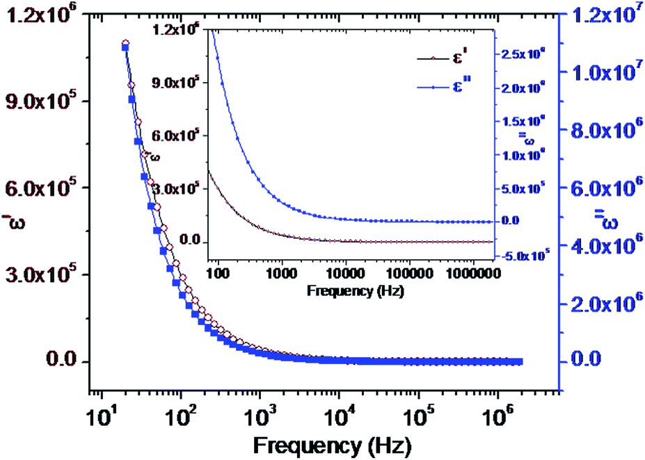 | ||
| Fig. 5 The real and imaginary parts of the dielectric constant of GO with frequency (shown from 20 Hz) at room temperature. | ||
Furthermore, the dielectric behavior of GO was also studied with varying temperature (30–180 °C) at a particular frequency, since it starts to lose weight beyond 200 °C. Fig. 6 shows a comparison of the dielectric behavior of a GO sample at various constant frequencies with the increase in temperature. We observe that the value of ε′ decreases with the increase in frequency. At 30 °C, the dielectric constant for 1 kHz is ∼35000, and with an increase in temperature it initially increases to ∼40000 (100 °C), and then decreases to ∼20000 (180 °C) due to the thermal vibration of chemical bonds, as well as due to the change in the dipole moment and orientation polarization of the functional groups (–OH and –COOH). A similar trend is also observed for all the other frequencies in the same temperature domain. However, with an increase in frequency, the dipoles cannot orient in a high applied alternating field and at higher temperatures and, subsequently, this results in the dielectric losses (see Fig. 6(a) and (b)). At higher temperature, GO loses its thermal stability, due to the degradation and loss of moisture CO, and CO2 due to the thermal degradation of the functional groups (–OH and –COOH) (see the TGA results, Fig. 3, S11 and S12†) and this is an expected common frequency-dependent dielectric phenomenon of almost all insulating thermally low stable dielectric materials.
 | ||
| Fig. 6 The dielectric dispersion of GO (a) for 1, 5, 50 and 100 KHz (b) for 0.5, 1.0, 1.5 and 2 MHz with increase in temperature. Inset of (a) shows enlarged view for 50 KHz and 100 KHz. | ||
There may be an obvious reason why the dielectric constant of GO initially increases with temperature for a particular frequency. The reason could be that, at a constant frequency, as the temperature increases a sudden increase in the dielectric constant is observed due to the reorientation/rearrangement of polarization of the functional groups present in the GO and thus a transition is observed due to the loss of absorbed moisture (TGA, see Fig. 3). Furthermore, the orientation/rearrangement of the attached functional groups (–OH and –COOH) present in the basal plan of GO result in a low dielectric constant at higher temperatures and frequencies.
The dispersion of the dielectric constant as a function of frequency was studied34,35 at various temperatures (30–180 °C) and results are shown in Fig. 7. From Fig. 7, it is apparent that the dielectric constant is very high at the low frequency range and it decreases as the frequency increases. This is due to the ceasing of the contributions from different polarizations with the increase in the frequency. As shown in Fig. 7, the high value at low frequencies is not due to the interfacial polarization and the consequent decrease is due to non-cooperation of the molecular dipoles with alternating fields. The effects of temperature on the dielectric constant of GO are also clearly seen in Fig. 7. As the temperature increases, the initial dielectric constant value also decreases at lower frequencies. The higher temperature causes the thermal fluctuations/change of mode of the bond vibrations at the intermolecular distance, as well as at the dipoles, which restrict them to orient in the direction of the applied electric field.
 | ||
| Fig. 7 The dielectric dispersion of GO with frequency (shown from 103 Hz) at different temperatures. | ||
The dispersion of the dielectric constant with temperature was studied and also the temperature dependence of ionic conductivity was investigated by plotting ln(σ) vs. (1/T) at different frequencies, and is shown in Fig. 8. All the plots demonstrate an Arrhenius type of behavior. By calculating the slope of respective plots, the values of the activation energy (Ea) were calculated, and are presented in Table 1.
 | ||
| Fig. 8 Log(σ) versus 1/T plots and fitted curves of the GO sample at (A) 1 kHz, 5 kHz and 50 kHz; (B) 0.5 MHz, 1.0 MHz, 1.5 MHz and 2 MHz frequencies. | ||
| Sl. no. | Frequency (kHz) | Activation energy (Ea), eV |
|---|---|---|
| 1 | 1 | 1.15 |
| 2 | 5 | 0.78 |
| 3 | 50 | 0.88 |
| 4 | 500 | 0.64 |
| 5 | 1000 | 0.64 |
| 6 | 1500 | 0.59 |
| 7 | 2000 | 0.58 |
As the temperature increases the conductivity also increases for all the plots, irrespective of the frequency. This is due to the hopping of ions/π-electrons through the conjugated basal plane along the –CC– bonds of GO. There might also be some atomic (carbon) vacancies/defects existing on the basal plane of GO sheet like graphene,36,37 which can lead to the transportation of charges/ions, which in general happens in many ionic solid conductors, e.g., NaCl. The effect of frequency on ionic conductivity is also prominent for GO (see Fig. 8(b)), which reveals that the ionic conductivity is less at higher frequencies and follows a similar trend as the temperature increases. At lower temperatures, the molecular dipoles of GO due to the presence of the polar groups –OH and –COOH can easily be re-oriented according to the alternating field mechanism and, hence, the ionic conduction values are lower.
From Fig. 9(A), it is manifested that the dielectric loss (tanδ) decreases with the frequency. The reason for this is, as the frequency increases the dipoles cannot orient along the direction of the applied electric field, and thus the loss due to the moment of the charges is decreased. If we compare all the plots at different temperatures, the loss is highest at high temperature. This is due to the high thermal agitation/vibration of the dipoles on the GO basal plane. However, for all the frequencies, the loss is between 2 and 5 up to 80 °C. As the temperature decreases, the thermal agitation/vibration decreases and the loss is less. From Fig. 9(B), it is clear that as the temperature increases, the loss also increases, irrespective of the frequency.
 | ||
| Fig. 9 Plots of frequency versus tanδ at various temperatures (A), and temperature versus tanδ at various frequencies (B) of the GO sample. | ||
Impedance measurements were taken of the GO sample after making it into pellet, as mentioned in the experimental section. The impedance was recorded at different temperatures by varying the frequency.
The corresponding plot between the real part (Z′) and imaginary parts of the impedance (Z′′) is shown in Fig. 10 as a representative plot obtained at RT. Plots for the other temperatures are shown in the ESI (Fig. S3 to S11†). The plots showing combination of two semicircles, indicating the contribution from the basal planes and the attached functional groups of GO. Since it is not a poly-crystalline material, the grain and grain boundary contributions are not applicable here.
 | ||
| Fig. 10 The Cole–Cole plot of the GO sample at RT and the fitted curves (solid blue lines). | ||
The data is fitted to obtain various parameters using the following Cole–Cole eqn (1):
 | (1) |
| Sl. no. | Temperature (°C) | Ro value from Cole–Cole analysis in Ω | DC conductivity σDC (Ωm) |
|---|---|---|---|
| 1 | 20 | 25091 |
3.980 × 10⁻⁵ |
| 2 | 40 | 24665 |
4.05 × 10⁻⁵ |
| 3 | 60 | 22628 |
4.419 × 10⁻⁵ |
| 4 | 80 | 21506 |
4.640 × 10⁻⁵ |
| 5 | 100 | 22661 |
4.412 × 10⁻⁵ |
| 6 | 120 | 26514 |
3.771 × 10⁻⁵ |
| 7 | 140 | 30768 |
3.250 × 10⁻⁵ |
| 8 | 160 | 39279 |
2.245 × 10⁻⁵ |
| 9 | 180 | 51465 |
1.943 × 10⁻⁵ |
The Cole–Cole plots and corresponding fittings at each temperature are shown in the ESI (Fig. S3 to S11†). The obtained d.c. conductivity values are plotted against the temperature values and are shown in Fig. 11(a). From Fig. 11(a), it can be seen that the d.c. conductivity initially increases up to 80 °C, and then decreases until 180 °C.
 | ||
| Fig. 11 DC conductivity with varying temperature (a), and AC conductivity with varying frequency at particular temperatures (b) of the GO sample. | ||
The A.C. conductivity σac as a function of frequency was calculated using the following equation, and the plots are shown in Fig. 11(b).
 | (2) |
Z′ and Z′′ are the real and the imaginary parts of impedance, t is the thickness and A is the area of the sample. There is not much variation observed in the A.C. conductivity in the low frequency region, but at higher frequencies, there is one order of magnitude change in the conductivity for every 10 °C increase in temperature observed. At 2 MHz, for all the measurements, the A.C. conductivity is observed to be 1.8 × 10⁻² S m−1, while it is 2 × 10⁻³ S m−1 at 20 Hz. There is also a minor variation in the conductivity with temperature. As the temperature increases, an increase in the A.C. conductivity is observed. At 180 °C, as mentioned earlier, pyrolysis of GO occurs and GO is converted partially into rGO/graphene sheet as the result of degradation of the functional groups.39 So, a number of the sp3 hybridized basal functionalized carbon atoms are converted into the sp2 hybridized carbons and therefore the π-electron system is ultimately changed. This conversion of sp3 → sp2 predominantly occurs at the defective sites of the GO, because numerous simulations indicate that –OH, –COOH or other functional groups can easily be attached to the vacancy-type defect sites of a graphene/graphite sheet (see Schematic 1–3),40,41 along with the oxidation at the defect free sites (see Schematic 1(a) → (d) conversion for defect-free site oxidation), since, at the vacancy site, the π-electron density, as well as the reactivity, are more energetically favourable for oxidation.40,42,43 Now a question arises as to whether there is any contribution of defects for the colossal dielectric value of GO or not? The answer is yes and to determine the defect status of the GO sheet, we performed HRTEM. The HRTEM micrograph (see Fig. 12) shows that the nature of the defects of GO is similar to the graphene/surface of graphite,44 which are mostly of a non-hexagonal ring type bonding geometry (the white spots in Fig. 12 are the functional groups).28
 | ||
| Fig. 12 (a) and (b) HRTEM images of GO at low and high magnification, respectively. The white spots are the oxidized region of the sheet. | ||
We oxidized the micron-sized graphite sheet into 1–2 layered GO in the presence of the required chemicals using high energy ultrasound (20 kHz). However, there is a possibility of the formation of non-hexagonal ring type defects by the reconstruction of graphitic lattice/graphene, such as Stone–Wales (SW)45–47 types of defect (55-77 type), which can be further converted into the oxide form (GO), since the required defect formation energy is a few eV only (see the schematic representation, Fig. 13(b)–(e) conversion), and is the energetically favourable state.47 Moreover, we can assume that the single vacancy (SV) defects forming in GO are due to the removal of atoms from the lattice position by high energy ultrasound, which we used during the synthesis of GO and are energetically favourable for the oxidation (see Fig. 13(c)–(f) conversion), because the SV formation requires very less energy (Ef ∼ 1.3 eV).48,49 At the vacancy site there will be a change in the polarization on application of an electric field, which contributes to the high dielectric properties. Furthermore, in the honeycomb lattice system of the graphitic sheet, when we apply the ultrasound there is a possibility of the formation of SV defects, which will undergo a Jahn–Teller type of distortion, in which the system goes into a lower energy state and forms a non-degenerate energy state50,51 and this leads to the saturation of two dangling bonds out of the three from the missing atom. Under this condition, another dangling bond contributes to the high dielectric permittivity of GO, along with the contribution of the functional groups attached at the defect sites. Moreover, we cannot expect the existence of 3d defects in GO, since it is only one-two layers of carbon sheets (only 0.7 nm thick). Apart from this, there is a possibility for defects like one-dimensional line defects, as well as the presence of defects at the edge of the GO layer where the carbon atoms and the free hydrogen atoms are dangling, as shown in Fig. 14 (see Fig. 14(a)). Furthermore, different types of reconstructions of graphite layers at the edges are possible, as shown in Fig. 14(b) and (c)). All these defects are very prone to chemical oxidation. These oxide forms of GO are shown in Fig. 14(d)–(f), and these also contribute to the change in the polarization, as well as to the dielectric permittivity. Furthermore, we cannot avoid the formation of defects in the bilayer GO. Bilayer GO consists of stacked two monolayers (as shown from the thickness of the AFM results, see Fig. 1(c)). Similar to with graphite, the inter-layer distance between adjacent bilayer GOs is approximately 3.35 Å, and is determined by the weak van der Waals forces of interactions between the adjacent GO layers and the defects present in both the layers. Again, we cannot avoid the formation of covalent inter-layer bonds during the formation of GO when the adatoms are located between the bi-layers/adjacent layers.52 These covalent inter-layer bonds lead to the creation of Frenkel-pairs (adatom–vacancy complexes) in one layer and change the hybridization of the adjacent layer, so that opposite carbon atoms from the two layers get connected (i.e., bridging of bonds) via one extra carbon atom.52 Such defects are also important for changes in the polarization of the GO and add to the high dielectric constant. Many other different types of defects can also be present in GO-like graphene shown in Fig. 15, and which can cause disturbance of the electron transport/delocalization and are also responsible for the colossal dielectric permittivity of the GO.36 Due to the defective GO basal plane and due to the Sp2–Sp3 conversion after functionalization with –OH, –COOH etc., π → π transitions of electrons are restricted, which hence decreases the conductivity of GO compared to the graphene/or few-layered graphene, and, as a result, increases the dielectric constant. In conclusion, the obtained dielectric constant value is superior compared to the reported results for rGO/Cl-rGO/r-GO-polymer composites in the same frequency range.24,53 Reduced graphene oxide have fewer oxygen containing functional groups and thus has a very much lower dielectric constant value, since it is conducting in nature and cannot be anticipated to be a good insulator/dielectric material according to literature.54,55 Furthermore, to study the role of the defects on the dielectric constant of GO, we performed a series of experiments, and the results are shown in the ESI (see Fig. S14†), which revealed that GO that was not sonicated during oxidation (GOL) had a lower value for the dielectric constant in the same frequency range. Fig. S15† provides evidence of the lower oxidation of GO (GOL).
 | ||
| Fig. 13 Schematic showing single-layered graphene, (a) defect free, (b) with 55-77 types of defect, and (c) with defect single vacancy 5-9 type; (d), (e) and (f) are their oxidized forms, respectively. | ||
 | ||
| Fig. 14 Schematic showing the single-layered graphene, (a) with a line defect, (b) with armchair reconstructed form, and (c) with defect 67 and 667 type; (d), (e) and (f) are their oxidized forms, respectively. | ||
 | ||
| Fig. 15 Schematic showing the single-layered graphene, (a) defect type 5-8-5, (b) defect type 555-777, and (c) defect type 5555-7777; (d), (e) and (f) are their oxidized forms, respectively. | ||
4. Conclusions
In summary, a new single/few-layered GO was synthesized by a modified Hammer's method and by using a sonochemical approach. Systematic investigations were performed to study the dielectric behavior of GO. Novel GO contains mainly –OH and –COOH functional groups, which are responsible for the change in polarization of GO sheets under the applied electric fields at the various frequency and temperature ranges. The present study strongly concluded that the novel GO exhibits a very high dielectric constant, which is in the order of 106 in magnitude. This value is very high, and is even very high compared to the conventional high dielectric materials such as CaCu3Ti4O12. It is hypothesized that the reorientation/rearrangement of the attached functional groups (–OH and –COOH) in the GO resulted in a change in the dipole moment and in the polarization, which lead to the high dielectric constant at low temperature and in a low frequency range. The contribution of the defects to the high dielectric value of GO were also addressed. All the defects are very prone to chemical oxidation of the single-layered graphite/graphene. These defects cause a restriction of the π → π transition of electrons and give rise to a strong dipole at the defect sides, resulting in an extraordinarily high value of dielectric constant with relatively low dielectric losses. This newly synthesized GO with a colossal dielectric constant is likely to enable us to further scale up advances in the performance of electronic and energy storage devices.References
- C. C. Homes and T. Vogt, Nat. Mater., 2013, 12, 782–783 CrossRef CAS PubMed.
- X. Hao, J. Adv. Dielectr., 2013, 03, 1330001 CrossRef.
- H. Xu and L. Gao, J. Am. Ceram. Soc., 2003, 86, 203–205 CrossRef CAS PubMed.
- M. A. Subramanian, D. Li, N. Duan, B. A. Reisner and A. W. Sleight, J. Solid State Chem., 2000, 151, 323–325 CrossRef CAS.
- A. P. Ramirez, M. A. Subramanian, M. Gardel, G. Blumberg, D. Li, T. Vogt and S. M. Shapiro, Solid State Commun., 2000, 115, 217–220 CrossRef CAS.
- C. C. Homes, T. Vogt, S. M. Shapiro, S. Wakimoto and A. P. Ramirez, Science, 2001, 293, 673–676 CrossRef CAS PubMed.
- S.-Y. Chung, I.-D. Kim and S.-J. L. Kang, Nat. Mater., 2004, 3, 774–778 CrossRef CAS PubMed.
- L. He, J. B. Neaton, M. H. Cohen, D. Vanderbilt and C. C. Homes, Phys. Rev. B: Condens. Matter Mater. Phys., 2002, 65, 214112 CrossRef.
- L. He, J. B. Neaton, D. Vanderbilt and M. H. Cohen, Phys. Rev. B: Condens. Matter Mater. Phys., 2003, 67, 12103 CrossRef.
- C. C. Homes, T. Vogt, S. M. Shapiro, S. Wakimoto, M. A. Subramanian and A. P. Ramirez, Phys. Rev. B: Condens. Matter Mater. Phys., 2003, 67, 92106 CrossRef.
- D. C. Sinclair, T. B. Adams, F. D. Morrison and A. R. West, Appl. Phys. Lett., 2002, 80, 2153–2155 CrossRef CAS PubMed.
- T. B. Adams, D. C. Sinclair and A. R. West, Adv. Mater., 2002, 14, 1321–1323 CrossRef CAS.
- W. Si, E. M. Cruz, P. D. Johnson, P. W. Barnes, P. Woodward and A. P. Ramirez, Appl. Phys. Lett., 2002, 81, 2056–2058 CrossRef CAS PubMed.
- L. Chen, C. L. Chen, Y. Lin, Y. B. Chen, X. H. Chen, R. P. Bontchev, C. Y. Park and A. J. Jacobson, Appl. Phys. Lett., 2003, 82, 2317–2319 CrossRef CAS PubMed.
- W. Hu, Y. Liu, R. L. Withers, T. J. Frankcombe, L. Norén, A. Snashall, M. Kitchin, P. Smith, B. Gong, H. Chen, J. Schiemer, F. Brink and J. Wong-Leung, Nat. Mater., 2013, 12, 821–826 CrossRef CAS PubMed.
- D. R. Dreyer, S. Park, C. W. Bielawski and R. S. Ruoff, Chem. Soc. Rev., 2010, 39, 228–240 RSC.
- H. He, J. Klinowski, M. Forster and A. Lerf, Chem. Phys. Lett., 1998, 287, 53–56 CrossRef CAS.
- C. Gómez-Navarro, R. T. Weitz, A. M. Bittner, M. Scolari, A. Mews, M. Burghard and K. Kern, Nano Lett., 2007, 7, 3499–3503 CrossRef PubMed.
- H. Chen, M. B. Müller, K. J. Gilmore, G. G. Wallace and D. Li, Adv. Mater., 2008, 20, 3557–3561 CrossRef CAS.
- Y. Bai, Y. Cao, J. Zhang, M. Wang, R. Li, P. Wang, S. M. Zakeeruddin and M. Gratzel, Nat. Mater., 2008, 7, 626–630 CrossRef CAS PubMed.
- T. Ramanathan, A. A. Abdala, S. Stankovich, D. A. Dikin, M. H. Alonso, R. D. Piner, D. H. Adamson, H. C. Schniepp, X. Chen, R. S. Ruoff, S. T. Nguyen, I. A. Aksay, R. K. Prud'Homme and L. C. Brinson, Nat. Nanotechnol., 2008, 3, 327–331 CrossRef CAS PubMed.
- S. Stankovich, D. A. Dikin, G. H. B. Dommett, K. M. Kohlhaas, E. J. Zimney, E. A. Stach, R. D. Piner, S. T. Nguyen and R. S. Ruoff, Nature, 2006, 442, 282–286 CrossRef CAS PubMed.
- T. K. Gupta, B. P. Singh, V. N. Singh, S. Teotia, A. P. Singh, I. Elizabeth, S. R. Dhakate, S. K. Dhawan and R. B. Mathur, J. Mater. Chem. A, 2014, 2, 4256–4263 CAS.
- J.-Y. Kim, W. H. Lee, J. W. Suk, J. R. Potts, H. Chou, I. N. Kholmanov, R. D. Piner, J. Lee, D. Akinwande and R. S. Ruoff, Adv. Mater., 2013, 25, 2308–2313 CrossRef CAS PubMed.
- J.-Y. Wang, S.-Y. Yang, Y.-L. Huang, H.-W. Tien, W.-K. Chin and C.-C. M. Ma, J. Mater. Chem., 2011, 21, 13569–13575 RSC.
- L. J. Romasanta, M. Hernández, M. a. López-Manchado and R. Verdejo, Nanoscale Res. Lett., 2011, 6, 508 CrossRef PubMed.
- P. Fan, L. Wang, J. Yang, F. Chen and M. Zhong, Nanotechnology, 2012, 23, 365702 CrossRef PubMed.
- N. R. Wilson, P. A. Pandey, R. Beanland, R. J. Young, I. A. Kinloch, L. Gong, Z. Liu, K. Suenaga, J. P. Rourke, S. J. York and J. Sloan, ACS Nano, 2009, 3, 2547–2556 CrossRef CAS PubMed.
- F. Tuinstra, J. Chem. Phys., 1970, 53, 1126 CrossRef CAS PubMed.
- a. Ferrari and J. Robertson, Phys. Rev. B: Condens. Matter Mater. Phys., 2000, 61, 14095–14107 CrossRef CAS.
- S. Stankovich, D. A. Dikin, R. D. Piner, K. A. Kohlhaas, A. Kleinhammes, Y. Jia, Y. Wu, S. T. Nguyen and R. S. Ruoff, Carbon, 2007, 45, 1558–1565 CrossRef CAS PubMed.
- S. Some, Y. Kim, E. Hwang, H. Yoo and H. Lee, Chem. Commun., 2012, 48, 7732–7734 RSC.
- D. Yang, A. Velamakanni, G. Bozoklu, S. Park, M. Stoller, R. D. Piner, S. Stankovich, I. Jung, D. A. Field, C. A. Ventrice Jr and R. S. Ruoff, Carbon, 2009, 47, 145–152 CrossRef CAS PubMed.
- J. Gass, P. Poddar, J. Almand, S. Srinath and H. Srikanth, Adv. Funct. Mater., 2006, 16, 71–75 CrossRef CAS.
- P. Suresh and S. Srinath, J. Alloys Compd., 2013, 554, 271–276 CrossRef CAS PubMed.
- F. Banhart, J. Kotakoski and A. V. Krasheninnikov, ACS Nano, 2011, 5, 26–41 CrossRef CAS PubMed.
- A. Lherbier, S. M.-M. Dubois, X. Declerck, Y.-M. Niquet, S. Roche and J.-C. Charlier, Phys. Rev. B: Condens. Matter Mater. Phys., 2012, 86, 75402 CrossRef.
- A. Sendilkumar, K. C. J. Raju, P. D. Babu and S. Srinath, J. Alloys Compd., 2013, 561, 174–179 CrossRef CAS PubMed.
- A. Lerf, H. He, M. Forster and J. Klinowski, J. Phys. Chem. B, 1998, 102, 4477–4482 CrossRef CAS.
- D. W. Boukhvalov and M. I. Katsnelson, Nano Lett., 2008, 8, 4373–4379 CrossRef CAS.
- G. Cantele, Y.-S. Lee, D. Ninno and N. Marzari, Nano Lett., 2009, 9, 3425–3429 CrossRef CAS PubMed.
- X. Peng and R. Ahuja, Nano Lett., 2008, 8, 4464–4468 CrossRef CAS PubMed.
- E. J. Duplock, M. Scheffler and P. J. D. Lindan, Phys. Rev. Lett., 2004, 92, 225502 CrossRef.
- F. Banhart, J. Kotakoski and A. V. Krasheninnikov, ACS Nano, 2011, 5, 26–41 CrossRef CAS PubMed.
- A. J. Stone and D. J. Wales, Chem. Phys. Lett., 1986, 128, 501–503 CrossRef CAS.
- L. Li, S. Reich and J. Robertson, Phys. Rev. B: Condens. Matter Mater. Phys., 2005, 72, 184109 CrossRef.
- J. Ma, D. Alfè, A. Michaelides and E. Wang, Phys. Rev. B: Condens. Matter Mater. Phys., 2009, 80, 33407 CrossRef.
- A. V. Krasheninnikov, P. O. Lehtinen, A. S. Foster and R. M. Nieminen, Chem. Phys. Lett., 2006, 418, 132–136 CrossRef CAS PubMed.
- A. A. El-Barbary, R. H. Telling, C. P. Ewels, M. I. Heggie and P. R. Briddon, Phys. Rev. B: Condens. Matter Mater. Phys., 2003, 68, 144107 CrossRef.
- M. H. Gass, U. Bangert, A. L. Bleloch, P. Wang, R. R. Nair and A. K. Geim, Nat. Nanotechnol., 2008, 3, 676–681 CrossRef CAS PubMed.
- J. C. Meyer, C. Kisielowski, R. Erni, M. D. Rossell, M. F. Crommie and A. Zettl, Nano Lett., 2008, 8, 3582–3586 CrossRef CAS PubMed.
- R. H. Telling, C. P. Ewels, A. A. El-Barbary and M. I. Heggie, Nat. Mater., 2003, 2, 333–337 CrossRef CAS PubMed.
- D. Wang, X. Zhang, J.-W. Zha, J. Zhao, Z.-M. Dang and G.-H. Hu, Polymer, 2013, 54, 1916–1922 CrossRef CAS PubMed.
- I. Jung, D. A. Dikin, R. D. Piner and R. S. Ruoff, Nano Lett., 2008, 8, 4283–4287 CrossRef CAS PubMed.
- H. Liu, L. Zhang, Y. Guo, C. Cheng, L. Yang, L. Jiang, G. Yu, W. Hu, Y. Liu and D. Zhu, J. Mater. Chem. C, 2013, 1, 3104–3109 RSC.
Footnote |
| † Electronic supplementary information (ESI) available: Table S1(a) Elemental analysis for GO, Fig. S1: EDX spectra of Graphene oxide, Fig. S2: Photographic image of GO pellet, Fig. S3–S11: Cole–Cole plots of GO at various temperatures with fitted curves, Fig. S12: TGA plot with derivative of graphite and Fig. S13: TGA plot with derivative of GO, Table S2: Elemental analysis for GOL, Fig. S14 for dielectric results for GOL, Fig. S15 EDX of GOL. See DOI: 10.1039/c4ra10800k |
| This journal is © The Royal Society of Chemistry 2015 |