Ni/Au hybrid nanoparticle arrays as a highly efficient, cost-effective and stable SERS substrate

Qun Fua, Kin Mun Wongb, Yi Zhoua, Minghong Wu*a and Yong Lei*ab
aInstitute of Nanochemistry and Nanobiology, School of Environmental and Chemical Engineering, Shanghai University, Shanghai, 200444, P. R. China.. E-mail: mhwu@shu.edu.cn; Fax: +86-21-66136898; Tel: +86-21-66137801
bInstitute for Physics and IMN MacroNano® (ZIK), Technical University of Ilmenau, Prof. Schmidt Str. 26, 98693 Ilmenau, Germany. E-mail: yong.lei@ilmenau.de; Fax: +49-0367769-3746; Tel: +49-0367769-3748

Received 26th August 2014 , Accepted 15th December 2014

First published on 15th December 2014


Abstract

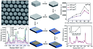
A large-area cost-effective Ni/Au hybrid nanoparticle array is synthesized with a proposed versatile and simple process by depositing Au on the pre-prepared arrays of Ni particles with ultra-thin alumina membranes as shadow mask during the deposition. A highly efficient and stable surface enhancement Raman scattering (SERS) substrate could be obtained from utilizing the resulting regular pattern of Ni/Au NP arrays. As compared with the single Au NP arrays, a largely decreased Au evaporation thickness and much lesser Au is needed for achieving the same Raman enhancement factor for the Ni/Au NP arrays. Subsequent SERS spectra measurement of the crystal violet (CV) molecule detection indicate a good SERS-active sensitivity with a detection limit of 10−10 M concentration, a large Raman enhancement factor at 108 was obtained, excellent SERS signal reproducibility with a relative standard deviation (RSD) as low as 6–7% as well as a great long term stability at 10 months.


1. Introduction

Large-scale surface nanoparticle (NP) patterns of noble metals (mainly Ag and Au) are good SERS substrates for bio-detection or bio-sensing due to their unique properties such as the high controllability of particle size, shape and interparticle spacing, high structure uniformity and hence the excellent reproducibility of SERS signal as well as the ideal repeatability of sample batches.1–6 Among the common fabrication methods of ordered NP arrays such as electron beam lithography (EBL),5,7–9 nanosphere lithography (NSL)10–13 and template-assisted nanopatterning technology,1,2,14–20 the UTAM (ultra-thin alumina membranes) surface fabrication technique21–25 provides an efficient nano-patterning process to prepare large-scale ordered arrays of NPs, and has been used recently to prepare Au and Ag NP arrays for SERS substrates. Normally the UTAM-assisted Au and Ag NP arrays are realized using the thermal evaporation process. At the beginning of the evaporation process, the particles are discrete particles that consist of a few very small metallic crystallites. With the progress of the evaporation process, the tiny crystallites cohere together and finally the discrete particle changes to a continuous particle where the evaporation thickness is one of the key factors for metal NP morphology. Hence the Raman enhancement effect of metal NP array SERS substrates largely depends on the thickness of the metallic particles when the size, interparticle distance, probing molecule and excitation wavelength are certain; especially the largest enhancement factor (EF) is obtained with a certain thickness (i.e., characteristic thickness ‘CT’) of particles. For the expensive metals in SERS substrate, it is crucial to make the CT as small as possible under the premise of achieving an ideal high SERS enhancement. To largely decrease the CT, we propose an innovative process by depositing Au on the pre-prepared Ni particles, so that the curved top surface of Ni particle shall slow down the cohering process, and hence largely enhance the SERS effect of the NPs array and thus effectively decrease the CT.

With our UTAM approach, the synthesized regular array of 25 nm Ni/20 nm Au hybrid NPs exhibit high uniformity and reproducibility. Convincing evidence was obtained from a Raman map which shows relatively uniform intensities of the SERS substrate on area of 10 × 10 μm2. Similarly, SERS signals taken at 15 randomly chosen locations across the sample demonstrated minimal variations in the characteristics peak intensities of the spectra with a period of 10 months between the measurements, hence verifying the long term stability of the Ni/Au composite arrays of NPs which is suitable for the detection of molecules. Importantly, our SERS substrate which was tested at molecule concentration ranging from 1 × 10⁻⁶ to 1 × 10⁻¹⁰ M also reveal evident SERS characteristics of the CV molecule at extremely low concentration at 10−10 M. Hence, this permits our synthesized hybrid metallic nanostructures for very sensitive and accurate detection of molecules at the low detection limit of 10−10 M. Furthermore, the 20 nm-thick Au layer on 25 nm-thick Ni particle arrays show a strong SERS effect comparable to the 45 nm-thick Au particle arrays, which means that the CT had been largely decreased. For achieving the same Raman enhancement, much lesser Au is needed and confirms the high cost-effectiveness of our innovative process.

It is well known that multicomponent nanoparticles can not only combine properties of the individual constituents but also show unique and superior properties which are different from ordinary materials, such as optical, catalytic, and photocatalytic properties.26–29 For instance, coating magnetic metals such as Fe, Co and Ni with Au not only provides advantages in surface protection and biocompatibility, but also exhibit unique optical properties such as surface plasmon resonance (SPR) and surface enhanced Raman scattering (SERS).30,31 Our SERS measurement results of CV adsorbed on the as-prepared 25 nm Ni/20 nm Au hybrid NP array SERS substrates show large SERS enhancement, great long-term stability and excellent reproducibility of the SERS signal, which indicates that the hybrid structure is a good candidate for analytical applications such as a biosensor.

2. Experimental

Fabrication of UTAMs

The UTAMs were prepared using a two-step anodization process.21,22 In brief, after a series of pretreatments, the high-purity (99.999%) aluminum foil with 0.2 mm thickness was first anodized in 0.3 M oxalic acid aqueous solution at 2 °C and under 40 V DC for 12 h. Then the anodic oxide layer was removed in a mixture of H3PO4 (6 wt%) and H2CrO4 (1.8 wt%) at 60 °C for about 10 h. The secondary anodization was carried out using the same solution and anodization voltage as the first step for 5 min, and then the Al back layer was removed in a CuCl2–HCl solution for about 10–20 minutes. The UTAMs with ordered channel arrays were obtained after a pore-widening process was carried out in phosphoric acid solution (5 wt%) at 30 °C for 65 min, and finally, the prepared UTAMs were attached on the Si substrate for subsequent usage.

Preparation of Ni/Au hybrid nanoparticle arrays

Ni was deposited on the UTAM/Si substrate by electron beam evaporation under the vacuum of 8 × 10⁻⁴ Pa with the electron gun voltage of 6 kV and current of 100–120 A. Subsequently, Au coating layer was thermally evaporated on the surface of Ni deposition in the UTAM channels with an evaporation voltage of 85 V and deposition rate of 0.3–0.5 nm s−1. After deposition of Au, the UTAM was stripped away using a tape, thus leaving behind the ordered Ni/Au hybrid nanoparticle arrays on the surface of the Si substrate. For fabrication of single Au nanoparticle array, Au was thermally evaporated on the UTAM/Si substrate under the same condition.

Preparation of samples for SERS measurement

All the Ni/Au hybrid NP arrays substrates for SERS measurements were prepared by immersion of the substrates in identical 1 × 10⁻⁶, 1 × 10⁻⁷, 1 × 10⁻⁸ and 1 × 10⁻¹⁰ M CV aqueous solution (30 ml) for 3 h to make sure that the surface were absorbed with a layer of CV molecules. For comparison, a bare Si substrate without metal deposition was directly immersed in the 1 × 10⁻³ M CV aqueous solution for 3 h to measure its normal Raman signal; pure Au NP arrays substrates with different Au thickness (10, 20, 30 and 45 nm) were immersed in 10−6 M CV aqueous solution for 3 h to measure their SERS signal. Subsequently, all the samples were rinsed with deionized water and dried by nitrogen gas flow. The sample stored for 10 months with 10−7 M CV molecules adsorbed was eluted by immersing the sample in absolute ethyl alcohol for a certain time period. Then the sample was immersed in the 10−7 M CV aqueous solution for 3 h to absorb the molecules again. According to the results of the pre-experiment, the immerse-dry sample has better SERS signal reproducibility comparing the drop-dry32 sample for our prepared nanostructure substrates. So here all the samples for SERS measurement were prepared by immersing-dry.

Characterization and SERS measurement

Scanning electron microscopy (SEM) images were obtained using a FE-SEM (JSM-6700 F, JEOL). The SERS spectra were collected by a 100× objective Renishaw System 1000 Raman spectrometer with a 633 nm wavelength He/Ne laser excitation in an exposure time of 10 s and the laser power was adjusted to 10%. All the SERS spectra were acquired from 5–6 different locations on the same sample and the ideal spectrum was reported. The baseline correction of the measured spectra was performed to remove the broad background and fluorescence band. SERS spectrum of the 10 month sample was measured directly. Subsequently, spectrum of the sample after elution desorption and after resorption treatment were carried out with the same route as mentioned above. Raman mapping was obtained by scanning the sample using step motors mounted on the microscope, with an area of 10 μm × 10 μm and a step length of 1 μm. All the experiments were performed in double or triplicate to check the reproducibility of the whole process.

3. Results and discussion

Fig. 1 schematically depicts the procedure for fabricating Ni/Au ordered hybrid NP arrays as SERS-active substrate using the UTAM as a template. Firstly, the UTAM was prepared using a two-step anodization process (I–II–III), and the prepared UTAM was transferred onto a silicon substrate (IV). Subsequently, Ni and Au were deposited on the Si substrate by electron beam and thermal evaporation successively in the vacuum condition using the UTAM as a shadow mask (V–VI). The nanostructure arrays are arranged by self-organized, hexagonally close packed nanochannels of the UTAM. After removing the UTAM, the regular Ni/Au hybrid NP arrays are obtained on the surface of the Si substrate (VII). Precise control over the sizes of the Ni/Au particles and the interparticle spacing between two adjacent particles is easily achieved by adjusting the structure parameters of the UTAM used as well as controlling the deposition condition (for example, the thickness of the Ni and Au layer and the deposition rate).
image file: c4ra09312g-f1.tif
Fig. 1 Schematic illustration of the process for fabricating the Ni/Au ordered hybrid nanoparticle arrays as SERS-active substrate with the UTAM as template. (I) First anodization of aluminum foil; (II) removal of the oxidized layer; (III) second anodization of aluminum foil; (IV) UTAM is transferred to the Si substrate after the aluminum back layer was removed and the pore-widening process; (V) deposition of Ni by electron beam evaporation with the UTAM as the shadow mask; (VI) thermal deposition of Au on the surface of Ni in the UTAM channels; (VII) Ni/Au ordered hybrid NP arrays after removing the UTAM.

Using the as-prepared UTAM (under a voltage of 40 V and with a pore-widening process of 65 min) as the shadow mask, three different evaporating thicknesses of Ni NP arrays were obtained, which were 10 nm, 15 nm and 25 nm respectively. As shown in the SEM images (shown in the ESI Fig. S1) of the Ni NP arrays, only at the 25 nm thickness, where the size of the Ni NP accords with the pore diameter (about 77 nm) of the UTAM. Conversely, at the thickness of 10 nm and 15 nm, the sizes of the Ni NPs (48 nm for 10 nm thickness and 60 nm for 20 nm thickness) are both far lesser than the UTAM pore size. Hence, 25 nm was used as the appropriate evaporating thickness of Ni in the Ni/Au ordered hybrid NP arrays during the sample preparation. On the surface of the Ni dot arrays in the UTAM channels, varying evaporation thickness of Au at 5 nm, 10 nm, 15 nm, 20 nm and 25 nm were deposited. Hence the ordered Ni/Au hybrid NP arrays were fabricated with various Au coating layer thickness, Ni/Au ratio and morphology. Fig. 2 shows the SEM images of six NP arrays of different evaporation thickness: 25 nm Ni (a), 25 nm Ni/5 nm Au (b), 25 nm Ni/10 nm Au (c), 25 nm Ni/15 nm Au (d), 25 nm Ni/20 nm Au (e) and 25 nm Ni/25 nm Au (f). From the figure, it was clearly observed that both Ni and Ni/Au NP arrays show high regularity and uniformity and are hexagonally close packed which is a replica of the UTAM nanopores. The 25 nm Ni nanoparticles (a) appear small and thin while the top surface is smooth. Accordingly, with the increasing Au layer thickness due to the deposition on the Ni particles, gradually the particles become plumper. A most important and interesting observation is that the top surface of the Ni particles is not smooth anymore, but becomes rougher [transiting from (b)–(c)–(d)–(e)] and then tends to be smooth again in (f). As shown in Fig. 2, when the Au deposition thickness increases to 10–20 nm [(c)–(d)–(e)], especially at 15 nm (d) and 20 nm (e), large amount of small crystallites (or discrete particles) assemble on the top surface of each particle and a spiny structure for the particle is clearly visible. However, as the Au coating layer thickness further increases to 25 nm (f), the discrete particles change to a continuous particle and the top surface turns out to be smooth and flat which is different from the thorn-like shape.


image file: c4ra09312g-f2.tif
Fig. 2 SEM images of 25 nm Ni NPs arrays (a), 25 nm Ni/5 nm Au (b), 25 nm Ni/10 nm Au (c), 25 nm Ni/15 nm Au (d), 25 nm Ni/20 nm Au (e) and 25 nm Ni/25 nm Au (f) hybrid NPs arrays.

In order to study how the SERS activity of the Ni/Au hybrid NPs depends on the thickness of the Au coating layer, SERS spectra of the CV molecules were measured on these prepared Ni/Au NP arrays with different Au layer thickness. Fig. 3A is the collection of the SERS spectra of 10−6 M CV absorbed on the NP arrays of 25 nm Ni, 25 nm Ni/5 nm Au, 25 nm Ni/10 nm Au, 25 nm Ni/15 nm Au, 25 nm Ni/20 nm Au and 25 nm Ni/25 nm Au. From the figure, it was clear that the spectrum (a) of the CV molecules obtained on the pure Ni nanoparticle arrays is so weak that almost no obvious CV vibration signal can be observed. However, as the Ni NP was coated with 5 nm Au (spectrum (b)), more vibrational modes can be obtained. With the further increase of the Au layer from 10 nm (c), 15 nm (d) to 20 nm (e), the SERS signal was enhanced remarkably. However, when the Au layer thickness was increased to 25 nm (f), the SERS signal does not continue to increase and was instead weaken. Therefore, the largest signal enhancement occurs when the thickness of the Au coating layer is 20 nm, i.e., the total hybrid particle thickness is 45 nm. Analogous SERS spectra measurement results of the 10−7 M CV in Fig. 3B also shows similar trend as the spectra of the 10−6 M CV. Fig. 3C clearly shows the dependence of the SERS peak intensity on the Au layer thickness of the Ni/Au hybrid NP for the 10−6 M CV molecule, which displays that the largest SERS enhancement occurs when the thickness of the Au layer is at 20 nm. Therefore, it can be seen that the Raman enhancement effect of the Ni/Au hybrid NP array as SERS substrates is largely dependent on the thickness of the Au deposition layer (or the thickness of the particle) when the size, shape, interparticle distance, probing molecule and excitation wavelength are experimentally determined. In particular, the largest enhancement factor is obtained with a certain thickness (i.e., characteristic thickness ‘CT’) of the particles. For the expensive metals in the SERS substrate, it is of great significance to make the CT as small as possible under the premise of achieving an ideal high SERS enhancement factor. We have demonstrated that depositing Au on the pre-prepared curved surface of the Ni NPs can largely enhance the SERS effect of the NPs array and thus effectively decrease the CT.


image file: c4ra09312g-f3.tif
Fig. 3 Collection of the SERS spectra of the 10−6 M (A) and the 10−7 M (B) CV molecules adsorbed on the NP arrays of 25 nm Ni (a), 25 nm Ni/5 nm Au (b), 25 nm Ni/10 nm Au (c), 25 nm Ni/15 nm Au (d), 25 nm Ni/20 nm Au (e) and 25 nm Ni/25 nm Au (f); (C) the dependence of SERS peak intensity on the Au layer thickness of the Ni/Au hybrid NP for 10−6 M CV molecule.

It was observed in Fig. 2 that the surface morphology of the Ni/Au NPs changes and the CT of the particles decrease. This can be explained by the deposition process of Au on the surface of the Ni nanoparticles. As shown in Fig. 4, on the curved top surface of the Ni NP that was pre-prepared with UTAM (Fig. 4a), Au was deposited with increasing thickness. When the Au evaporated thickness is very small (as shown in Fig. 4b), only a small amount of Au crystallites was sparsely deposited on the surface of the Ni NPs. Hence, the Au deposition layer is discrete which consist of a few very small metallic crystallites, and the surface roughness is higher as compared with the pure Ni particle surface. Due to the presence of the surface roughness and the strong coupling of surface plasmon between the adjacent Au crystallites, the Raman intensity of the CV molecules on the 25 nm Ni/5 nm Au hybrid NP arrays is evidently enhanced as compared with the pure Ni NP arrays. With the increase of the Au deposition thickness, more of the discrete particles will coalesce on the surface of the Ni NPs (Fig. 4c), thus resulting in large quantity of pinholes or gaps between the adjacent Au little particles on the hybrid NPs surface. As a result, the surface roughness will increase sharply, until the number of discrete particles and the pinholes or gaps becomes the largest (Fig. 4d) which result in the smallest size of the pinholes or gaps. Accordingly, due to the strong coupling between not only the tiny crystallites which have a lot of nanogaps but also between the neighboring Ni/Au NPs owing to an Au coating layer, the SERS intensity of the Ni/Au NPs will also subsequently enhance until the largest enhancement occurred at a certain thickness. However, when the Au coating layer thickness further increases, the pinholes or gaps on the surface will be gradually filled by more of the deposited Au crystallites and at the same time the tiny crystallites will cohere together. Finally, the Au discrete particles assemble into bigger and continuous Au particles, which results in the Ni NPs surface becoming densely covered with the Au layer and hence the surface tending to be smooth and flat (Fig. 4e). Therefore, the SERS signal enhancement does not continue to increase but will weaken instead. In other words, when the particle thickness is smaller than CT, although each particle consists of a few small crystallites (or discrete particle) which is favorable for Raman enhancement, however the small amount of evaporated metal limits the overall Raman enhancement. With further growth (in our case the thickness is increasing due to the pore confinement which limits their growth in the lateral direction) of the NPs, despite the increment of the SERS-active metal materials, the discrete particle will be transformed to a continuous particle and hence decreases the Raman enhancement.


image file: c4ra09312g-f4.tif
Fig. 4 Schematic illustration of the deposition process of Au small crystallite (SC) on the curved surface of the Ni nanoparticles [(a)–(b)–(c)–(d)–(e)] and the flat surface of the bare Si substrate [(a′)–(b′)–(c′)–(d′)] within the confinement of the UTAM pores, respectively.

For the UTAM technique in fabricating Au NPs, all the particles are usually grown on a flat place of the substrate (for example Si wafer, shown as Fig. 4a′). At the beginning of the deposition process, the particles are discrete (Fig. 4b′), and with the progress of the evaporation process, more of the Au particle tends to coalesce together (Fig. 4c′). On a flat surface, the small Au particles are more easily cohered and will assemble to be continuous with each other; hence the surface becomes continuous and smooth in a shorter time. But on the contrary, the curved top surface of the Ni particle will slow down the cohering process, hence the top surface of the Ni/Au hybrid particle will be inclined to sustain more discrete particles and result in a higher surface roughness after a certain period of time. Therefore, for the same Au deposition thickness on the curved and flat surface of the substrate, the SERS enhancement effect of the former will be much stronger than the latter. For the same level of enhancement of the SERS substrate, deposition on the curved surface shall largely decrease the CT, which is crucial for expensive metal (for example, Au) in fabricating cost-effective SERS substrate. To prove this point, pure Au NPs arrays with different thicknesses of 10, 20, 30 and 45 nm were fabricate by the same UTAM, and the SERS performances of being absorbed with 10−6 M CV molecule were compared with the 25 nm Ni/20 nm Au (the largest SERS enhancement substrate) hybrid NP arrays. Results are shown in Fig. 5 and as expected, for 10−6 M CV, the SERS signal enhancement of the 10 nm-thick pure Au NP arrays is extremely small, while the enhancement strengthens with the Au thickness increases from 10 nm to 45 nm. Moreover, when the Au thickness is less than 30 nm, the SERS enhancement is smaller than the 25 nm Ni/20 nm Au substrate. However, when the Au thickness increases to 45 nm, the SERS signal shows a strong SERS effect which is comparable to the 25 nm Ni/20 nm Au particle, especially for 1177 and 1619 cm−1 band (shown as Fig. 5). In other words, deposition of 25 nm Au on a curved surface of the Ni NP will result in the same level enhancement of the SERS signal as a 45 nm-thick Au particle, which means that the CT has been largely decreased. The calculated enhancement factors (EFs) (shown in ESI Table 1) for all the samples in Fig. 5 further prove quantitatively that the enhancement activity for 25 nm Ni/20 nm Au particle arrays and pure 45 nm-thick Au NP arrays are in the same level. Therefore, in achieving the same level of Raman enhancement, much lesser Au is needed which confirms the high cost-effectiveness of our proposed innovative process.


image file: c4ra09312g-f5.tif
Fig. 5 SERS spectra of the 10−6 M CV molecule on the 25 nm Ni/20 nm Au hybrid NP array substrate and pure Au particle array substrate with different thickness of 10, 20, 30 and 45 nm, and normal Raman spectroscopy.

In our results, the 25 nm Ni/20 nm Au hybrid NP array substrate shows remarkable SERS enhancement not only for 10−6 M CV, but also for 10−7, 10−8 M and even for very low concentration at 10−10 M. Fig. 6A displays the collection of spectra of the CV molecule with four different concentrations absorbed on the 25 nm Ni/20 nm Au hybrid NP array substrate [(a)–(d)] as well as the normal Raman spectrum of 10−3 M CV (e) on a bare Si substrate without metal deposition. As shown in Fig. 6A, nearly no Raman signal can be found for normal Raman measurement on the bare Si substrate, while for every other molecule concentration from 10−6, 10−7, 10−8 to 10−10 M, the SERS spectrum reveals the apparent characteristic signals of the CV molecule, even for the very low concentration at 10−10 M. Such successful detection for extremely low concentration indicates that the hybrid NP array substrate is a good trace probing substrate.


image file: c4ra09312g-f6.tif
Fig. 6 (A) Collection of spectra of the CV molecule with four different concentrations absorbed on the 25 nm Ni/20 nm Au hybrid NP array substrate [(a)–(d)] and the normal Raman spectrum of the 10−3 M CV molecule (e) on a bare Si substrate without metal deposition. (B) The dependence of the EFs on the thickness of the Au coating layer at 1177 cm−1 peak for the 10−10 M CV absorption. Inset shows the structure of the CV molecule.

For a qualitative evaluation of the SERS enhancement effect of the 25 nm Ni/20 nm Au hybrid NP array substrate, the enhancement factors, EFs, for 10−6, 10−7, 10−8 and 10−10 M CV molecules were estimated (details are in ESI Table 2). The dependence of EFs on the thickness of Au coating layer at 1177 cm−1 peak for the 10−10 M CV adsorption is shown in Fig. 6B. With the increase of the thickness of Au coating layer on the Ni/Au hybrid NPs, the EFs firstly increase and then decrease after reaching to the highest value of 4.5 × 10⁸ at 10−10 M concentration. As mentioned above, this great SERS enhancement can be mostly attributed to the strong coupling of the surface plasmon between the numerous Au discrete particles on the surface of Ni NPs as well as the large enhancement of the localized electromagnetic field in the nanogaps between adjacent Ni/Au NPs. Due to the close packing of the Ni/Au nanoparticles in a large area assembly by the UTAM (as shown in Fig. 2), this can lead to strong interparticle plasmon coupling. Additionally, in our fabricated Ni/Au hybrid NPs, the Au depositing particles are packed on the surface of the Ni NPs. The effect of the magnetic field of the Ni particles will lead to coupling between the top Au layer and the bottom Ni NPs and thus the Ni/Au hybrid NPs also exhibit ferromagnetic behavior. Therefore it is possible that the local electromagnetic field near the Au surface can be magnified because of the interaction between the magnetic Ni particles and the Au surface layer. This may be another component of the contribution to the strong SERS enhancement for the Ni/Au hybrid NP arrays which cannot be achieved in single Au NP arrays substrates. Magnetic effect of the Ni/Au composite NPs can make an impact on the surface electrons that influence the distribution of the adsorbed CV molecules. Therefore, the SERS effect of the adsorbed CV molecules is further enhanced and displays different vibrational modes from the Au NP as observed in Fig. 5.

Coating a certain thickness of Au layer on the surface of the Ni NPs can also prevent oxidization30 thus sustaining the long time stability of the Ni/Au hybrid NP arrays substrate especially in corrosive biological conditions. Fig. 7 shows the comparison of the SERS performance of the 10−7 M CV molecule adsorbed on three substrate samples: after 10 months storage (a), eluting desorption (b) and adsorption again after eluting desorption (c). Using the SERS intensity of the 1618 cm−1 peak as an example, for the sample after 10 months, the intensity still reaches 96.6% of that of the as-prepared sample [Fig. 3B(e)]. After eluting desorption, the SERS spectrum has almost no Raman signal of the CV molecule. When adsorbed in 10−7 M CV molecules again, the intensity of the 1618 cm−1 peak reaches 93% of the value obtained previously with eluting desorption. This small reduction of the SERS intensity demonstrated the long-term stability of the Ni/Au composite arrays due to the Au coating that prevents oxidization effectively, and thus the SERS substrate can be reused after 10 months or even a longer time.


image file: c4ra09312g-f7.tif
Fig. 7 SERS spectra of the 10−7 M CV molecule adsorbed on three substrate samples: after 10 months of storage (a), eluting desorption (b) and adsorption again after eluting desorption (c).

Many different SERS substrates have been reported in the literature but one of the problems that still remain unsolved is the reproducibility of the Raman enhancement spectra. One of the advantages of our method for SERS substrate fabrication by UTAM is that we can precisely control the structural parameters and uniformity of the NPs, hence the great reproducibility of the SERS signals can be obtained easily. To illustrate the surface homogeneity of the as-prepared NP arrays substrate and the reproducibility of the SERS activity, a Raman area map [Fig. 8A] was taken on an area of 10 × 10 μm2 and the SERS spectra [Fig. 8B] were taken from 15 different sites that are chosen randomly on the entire 1 cm2 area in the 25 nm Ni/20 nm Au substrate for the 10−6 M CV molecule. Fig. 8A displays two of the spot-to-spot SERS maps for different areas (10 × 10 μm2) in the substrate, which were recorded with a step of 1 μm using the integrated area of the baseline-corrected peaks at 1177 cm−1. The bright and dark colors distribution shows the SERS signal intensities tend to be uniform on the whole. As shown in Fig. 8B, for the spectra of 15 different locations that are chosen randomly in the sample, it can be observed that there are no changes in the characteristic peaks of the spectra except for very minimal variations in the intensity at various points. In order to prove the high reproducibility of the substrate, relative standard deviation (RSD) of the SERS intensity for 10−6 M CV on the 25 nm Ni/20 nm Au substrate at three prominent peaks at 1177, 1372, and 1618 cm−1 (7.0%, 6.9%, and 6.7%, respectively) was calculated and the standard deviation was shown in the inset of Fig. 8B. Base on these results, the 25 nm Ni/20 nm Au NP arrays substrates displayed excellent reproducibility of the SERS performance with low RSD values at 6–7%. The observed small intensity variation with high SERS enhancement in a large area (>1 cm2) is far below any of the previously reported substrates fabricated by other various techniques with RSD values in the range of 10–20%.33–36


image file: c4ra09312g-f8.tif
Fig. 8 (A) Selected SERS maps of the CV molecules (1177 cm−1, 10 × 10 μm2, step size 1 μm) on the 25 nm Ni/20 nm Au NPs substrate with the average intensities integrated. Scale bar: 2 μm; (B) spectra measured at 15 different regions on a 1 cm2 area of the 25 nm Ni/20 nm Au NP arrays. Variation in the SERS spectra was well below 7%. Inset shows the standard deviation and the average value of the three prominent peaks at 1177, 1372 and 1618 cm−1.

As mentioned above, coating of Au on the curved surface of the pre-prepared Ni NP not only can exhibit strong SERS enhancement but can also largely decrease the CT of the NP arrays. Therefore this reduces the amount of Au used and show the high cost-effectiveness of our proposed fabrication method. In fact, our method is not only applicable to Ni but can be readily extended to other metals such as Fe and Co. However, the different metal will have different CT and SERS effect.

4. Conclusions

In conclusion, a cost-effective Ni/Au hybrid nanoparticle arrays as highly efficient and stable SERS substrate was successfully fabricated by depositing Au on the pre-prepared Ni particles with the UTAM as the shadow mask. Our proposed method greatly decreased the needed Au thickness and much lesser Au is needed for achieving the same Raman enhancement. The as-prepared Ni/Au NP arrays substrate shows good sensitivity with a detection limit of 10−10 M of crystal violet molecule, excellent reproducibility with a low RSD at 6–7%, great long term stability for 10 months and large Raman enhancement factor as high as 108. The method was demonstrated to be effective for the development of cost-effective hybrid nanoparticle arrays to be used as highly efficient and stable SERS substrate for bio-sensing applications.

Acknowledgements

This work was supported by Program for Innovative Research Team in University (no. IRT13078), National Science Foundation of China (51301104), and European Research Council (ThreeDsurface: 240144), BMBF (ZIK-3DNanoDevice: 03Z1MN11) and BMBF (Meta-ZIK-BioLithoMorphie: 03Z1M511) in Germany.

References

  1. H. H. Wang, C. Y. Liu, S. B. Wu, N. W. Liu, C. Y. Peng, T. H. Chan, C. F. Hsu, J. K. Wang and Y. L. Wang, Highly Raman-Enhancing Substrates Based on Silver Nanoparticle Arrays with Tunable Sub-10 nm Gaps, Adv. Mater., 2006, 18, 491–495 CrossRef CAS.
  2. V. Liberman, C. Yilmaz, T. M. Bloomstein, S. Somu, Y. Echegoyen, A. Busnaina, S. G. Cann, K. E. Krohn, M. F. Marchant and M. A. Rothschild, Nanoparticle Convective Directed Assembly Process for the Fabrication of Periodic Surface Enhanced Raman Spectroscopy Substrates, Adv. Mater., 2010, 22, 4298–4302 CrossRef CAS PubMed.
  3. D. A. Genov, A. K. Sarychev, V. M. Shalaev and A. Wei, Resonant Field Enhancements from Metal Nanoparticle Arrays, Nano Lett., 2004, 4, 153–158 CrossRef CAS.
  4. Z. Zhu, H. Meng, W. Liu, X. Liu, J. Gong, X. Qiu, L. Jiang, D. Wang and Z. Tang, Superstructures and SERS Properties of Gold Nanocrystals with Different Shapes, Angew. Chem., Int. Ed., 2011, 50, 1593–1596 CrossRef CAS PubMed.
  5. H. Duan, H. Hu, K. Kumar, Z. Shen and J. K. W. Yang, Direct and Reliable Patterning of Plasmonic Nanostructures with Sub-10 nm Gaps, ACS Nano, 2011, 5, 7593–7600 CrossRef CAS PubMed.
  6. B. Yan, S. V. Boriskina and B. M. Reinhard, Design and Implementation of Noble Metal Nanoparticle Cluster Arrays for Plasmon Enhanced Biosensing, J. Phys. Chem. C, 2011, 115, 24437–24453 CAS.
  7. J. Theiss, P. Pavaskar, P. M. Echternach, R. E. Muller and S. B. Cronin, Plasmonic Nanoparticle Arrays with Nanometer Separation for High-Performance SERS Substrates, Nano Lett., 2010, 10, 2749–2754 CrossRef CAS PubMed.
  8. Y. Yokota, K. Ueno and H. Misawa, Essential Nanogap Effects on Surface-Enhanced Raman Scattering Signals from Closely Spaced Gold Nanoparticles, Chem. Commun., 2011, 47, 3505–3507 RSC.
  9. K. Ueno, S. Juodkazis, V. Mizeikis, K. Sasaki and H. Misawa, Clusters of Closely Spaced Gold Nanoparticles as a Source of Two-Photon Photoluminescence at Visible Wavelengths, Adv. Mater., 2008, 20, 26–30 CrossRef CAS.
  10. C. L. Haynes and R. P. Van Duyne, Nanosphere Lithography: A Versatile Nanofabrication Tool for Studies of Size-Dependent Nanoparticle Optics, J. Phys. Chem. B, 2001, 105, 5599–5611 CrossRef CAS.
  11. C. L. Hynes and R. P. Van Duyne, Plasmon-Sampled Surface-Enhanced Raman Excitation Spectroscopy, J. Phys. Chem. B, 2003, 107, 7426–7433 CrossRef.
  12. T. R. Jensen, G. C. Schatz and R. P. Van Duyne, Nanosphere Lithography: Surface Plasmon Resonance Spectrum of a Periodic Array of Silver Nanoparticles by Ultraviolet-Visible Extinction Spectroscopy and Electrodynamic Modeling, J. Phys. Chem. B, 1999, 103, 2394–2401 CrossRef CAS.
  13. X. Y. Zhang, C. R. Yonzon and R. P. Van Duyne, Nanosphere Lithography Fabricated Plasmonic Materials and Their Applications, J. Mater. Res., 2006, 21, 1083–1092 CrossRef CAS.
  14. H. Masuda and K. Fukuda, Ordered Metal Nanohole Arrays Made by a Two-Step Replication of Honeycomb Structures of Anodic Alumina, Science, 1995, 268, 1466–1468 CAS.
  15. Z. Luo, W. Yang, A. Peng, Y. Ma, H. Fu and J. Yao, Net-like Assembly of Au Nanoparticles as a Highly Active Substrate for Surface-Enhanced Raman and Infrared Spectroscopy, J. Phys. Chem. A, 2009, 113, 2467–2472 CrossRef CAS PubMed.
  16. M. Rycenga, P. H. C. Camargo and Y. Xia, Template-Assisted Self-Assembly: A Versatile Approach to Complex Micro- and Nanostructures, Soft Matter, 2009, 5, 1129–1136 RSC.
  17. B. Yan, A. Thubagere, W. R. Premasiri, L. D. Ziegler, L. D. Negro and B. M. Reinhard, Engineered SERS Substrates with Multiscale Signal Enhancement: Nanoparticle Cluster Arrays, ACS Nano, 2009, 3, 1190–1202 CrossRef CAS PubMed.
  18. A. Cerf, G. Molnar and C. Vieu, Novel Approach for the Assembly of Highly Efficient SERS Substrates, ACS Appl. Mater. Interfaces, 2009, 1, 2544–2550 CAS.
  19. S. J. Lee, Z. Guan, H. Xu and M. Moskovits, Surface-Enhanced Raman Spectroscopy and Nanogeometry: The Plasmonic Origin of SERS, J. Phys. Chem. C, 2007, 111, 17985–17988 CAS.
  20. M. Schierhorn, S. J. Lee, S. W. Boettcher, G. D. Stucky and M. Moskovits, Metal–Silica Hybrid Nanostructures for Surface-Enhanced Raman Spectroscopy, Adv. Mater., 2006, 18, 2829–2832 CrossRef CAS.
  21. M. H. Wu, L. Y. Wen, Y. Lei, S. Ostendorp, K. Chen and G. Wilde, Ultrathin Alumina Membranes for Surface Nanopatterning in Fabricating Quantum-Sized Nanodots, Small, 2010, 6, 695–699 CrossRef CAS PubMed.
  22. Y. Lei, W. P. Cai and G. Wilde, Highly ordered nanostructures with tunable size, shape and properties: a new way to surface nano-patterning using ultra-thin alumina masks, Prog. Mater. Sci., 2007, 52, 465–539 CrossRef CAS PubMed.
  23. Y. Lei, Z. Jiao, M. H. Wu and G. Wilde, Ordered Arrays of Nanostructures and Applications in High-Efficient Nano-Generators, Adv. Eng. Mater., 2007, 9, 343–348 CrossRef CAS.
  24. Z. Chen, Y. Lei, H. G. Chew, L. W. Teo, W. K. Choi and W. K. Chim, Synthesis of Germanium Nanodots on Silicon Using an Anodic Alumina Membrane Mask, J. Cryst. Growth, 2004, 268, 560–563 CrossRef CAS PubMed.
  25. Y. Lei, W. K. Chim, Z. P. Zhang, T. J. Zhou, L. D. Zhang, G. W. Meng and F. Phillipp, Ordered nanoporous nickel films and their magnetic properties, Chem. Phys. Lett., 2003, 380, 313–318 CrossRef CAS PubMed.
  26. X. Hou, X. Zhang, S. Chen, H. Kang and W. Tan, Facile Synthesis of Ni/Au, Ni/Ag Hybrid Magnetic Nanoparticles: New Active Substrates for Surface Enhanced Raman Scattering, Colloids Surf., A, 2012, 403, 148–154 CrossRef CAS PubMed.
  27. E. V. Shevchenko, M. I. Bodnarchitk, M. V. Kovalenko, D. V. Talapin, R. K. Smith, S. Aloni, W. Heiss and A. P. Alivisatos, Gold/Iron Oxide Core/Hollow-Shell Nanoparticles, Adv. Mater., 2008, 20, 4323–4329 CrossRef CAS.
  28. Y. Lee, M. A. Garcia, N. A. Frey Huls and S. Sun, Synthetic Tuning of the Catalytic Properties of Au–Fe3O4 Nanoparticles, Angew. Chem., Int. Ed., 2010, 49, 1271–1274 CrossRef CAS PubMed.
  29. D. Wang and Y. Li, One-Pot Protocol for Au-Based Hybrid Magnetic Nanostructures via a Noble-Metal-Induced Reduction Process, J. Am. Chem. Soc., 2010, 132, 6280–6281 CrossRef CAS PubMed.
  30. H. She, Y. Chen, X. Chen, K. Zhang, Z. Wang and D. L. Peng, Structure, Optical and Magnetic Properties of Ni@Au and Au@Ni Nanoparticles Synthesized via Non-aqueous Approaches, J. Mater. Chem., 2012, 22, 2757–2765 RSC.
  31. Z. Xu, Y. Hou and S. Sun, Magnetic Core/Shell Fe3O4/Au and Fe3O4/Au/Ag Nanoparticles with Tunable Plasmonic Properties, J. Am. Chem. Soc., 2007, 129, 8698–8699 CrossRef CAS PubMed.
  32. Y. Yang, Z.-Y. Li, K. Yamaguchi, M. Tanemura, Z. Huang, D. Jiang, Y. Chen, F. Zhou and M. Nogamic, Controlled fabrication of silver nanoneedles array for SERS and their application in rapid detection of narcotics, Nanoscale, 2012, 4, 2663–2669 RSC.
  33. J. D. Driskell, S. Shanmukh, Y. Liu, S. B. Chaney, X. J. Tang, Y. P. Zhao and R. A. Dluhy, The Use of Aligned Silver Nanorod Arrays Prepared by Oblique Angle Deposition as Surface Enhanced Raman Scattering Substrates, J. Phys. Chem. C, 2008, 112, 895–901 CAS.
  34. J. Zhou, S. Xu, W. Xu, B. Zhao and Y. Ozaki, In situ Nucleation and Growth of Silver Nanoparticles in Membrane Materials: A Controllable Roughened SERS Substrate with High Reproducibility, J. Raman Spectrosc., 2009, 40, 31–37 CrossRef CAS.
  35. M. A. Khan, T. P. Hogan and B. Shanker, Gold-coated zinc oxide nanowire-based substrate for surface-enhanced Raman spectroscopy, J. Raman Spectrosc., 2009, 40, 1539–1545 CrossRef CAS.
  36. X.-M. Lin, Y. Cui, Y.-H. Xu, B. Ren and Z.-Q. Tian, Surface-Enhanced Raman Spectroscopy: Substrate-Related Issues, Anal. Bioanal. Chem., 2009, 394, 1729–1745 CrossRef CAS PubMed.

Footnote

Electronic supplementary information (ESI) available. See DOI: 10.1039/c4ra09312g

This journal is © The Royal Society of Chemistry 2015