The optimization of electric properties of multilayered BNT–BT–ST/BCST thin films by configuration

Wei Liab, Peng Lia, Huarong Zengc, Jigong Haoab and Jiwei Zhai*a
aFunctional Materials Research Laboratory, School of Materials Science and Engineering, Tongji University, Shanghai 201804, China. E-mail: apzhai@tongji.edu.cn
bSchool of Materials Science and Engineering, Liaocheng University, Liaocheng 252059, China. E-mail: liwei_727@163.com
cKey Laboratory of Inorganic Functional Materials and Devices, Shanghai Institute of Ceramics, Chinese Academy of Sciences, Shanghai 200050, China. E-mail: huarongzeng@mail.sic.ac.cn

Received 29th October 2014 , Accepted 4th December 2014

First published on 4th December 2014


Abstract

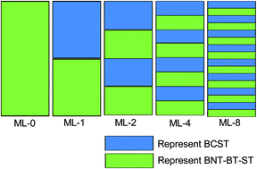
The 0.755Bi0.5Na0.5TiO3–0.065BaTiO3–0.18SrTiO3/Ba0.98Ca0.02Ti0.96Sn0.04O3 (BNT–BT–ST/BCST) multilayered thin films, consisting of BNT–BT–ST layers and BCST layers, were prepared by using the sol–gel processing technique. The structure, leakage current, dielectric and piezoelectric properties of the multilayered thin films were investigated. Compositionally graded elemental profiles between individual BNT–BT–ST and BCST layers were achieved. The electric properties of the BNT–BT–ST/BCST multilayered thin films could be affected by the periodic layers. As a result, with an increase in periodic layers of the BNT–BT–ST/BCST multilayered thin films, the leakage current and dielectric loss were significantly reduced; moreover, the piezoelectric responses could be maintained at a high level (d33 = 130–150 pm V−1). This demonstrated the possibility to improve certain properties of the leakage current and dielectric loss for multilayered thin films, which could be exploited for functional devices that demand high quality.


Introduction

Contemporary high-precision micropositioning systems and sensors rely on the outstanding electromechanical properties exhibited by lead zirconate titanate (PZT)-based solid solutions. Nevertheless, from a health perspective, the manipulation of toxic lead oxide during the fabrication of PZT-based components and their later disposal partially overshadows its technological merits. In consideration of the growing demand for green materials with minimized impacts on health and environment, researchers are making intensive efforts to replace lead-based materials with lead-free compositions.1,2

Among the lead-free materials, bismuth sodium titanate (BNT)-based materials have seen a flurry of research interest in recent years because of the existence of extended strain under applied electric fields. Recently, a large strain response of 0.2% (Smax/Emax = 490 pm V−1) at a driving field of 4 kV mm−1 was obtained in the Bi0.5Na0.5TiO3–BaTiO3–SrTiO3 (BNT–BT–ST) system.3–5 Many studies have reported that the large strain obtained in ABO3-modified BNT-based materials could be due to the composition induced ferroelectric-relaxor phase transition. The enhancement of the strain in these materials is accompanied by the disruption of ferroelectric order, and corresponded to the ferroelectric-to-relaxor transition point at nearly room temperature.6–8 The processing and properties of ternary BNT-based single crystals and ceramics have been innovatively developed. In contrast to the numerous studies on BNT-based bulk materials, BNT-based thin films have not been studied extensively. Piezoelectric thin films offer a number of advantages in micro-electromechanical systems (MEMS), and the preparation and characterization of piezoelectric thin films are hot topics in the present microelectronic industry.9,10 The lack of progress in BNT-based thin films may be attributed to the challenges associated with the deposition of high-quality thin films. The inherent properties are accompanied by some commonly encountered difficulties, such as high conductivity, large dielectric loss and coercive field in the poling process of NBT-based films. The increased conductivity could be related to the nonstoichiometry, arising from high volatility of Na and Bi cations during processing. Enormous efforts have been undertaken to innovate new piezoelectric films and improve their properties by varying the compositions and shapes.11,12 As a result, both composition and configuration have significant influences on the electric properties of the thin films.13 In terms of configuration, three basic models have been considered: (i) layered structure with layers of the two components alternatively connected in series (2–2 type), (ii) parallel columnar structure of one phase embedded within the matrix of the other phase (1–3 type), and (iii) random distribution with one phase as spheres embedded into another as matrix (3–0 type).14 Furthermore, reduced leakage currents and improved electrical fatigue characteristics were obtained in biphasic composition multilayered thin films of PbZrxTi1−xO3/PbZrO3 and PbZrxTi1−xO3/SrBi2Ta2O3, respectively.15,16

Considering the leakage current and dielectric behavior of piezoelectric materials, the BCST system appears as particularly intriguing due to its exclusive volatility and high piezoelectric properties (d33 = 300–600 pC/N). The high piezoelectric properties, in the BCST system, are rationalized with the existence of a polymorphic phase transition (PPT) between orthorhombic and tetragonal phases.17,18 The investigations on NBT-based films focus on improving the inherent piezoelectric behavior and reducing the conductivity during polarization progress. In this attempt, the BNT–BT–ST/BCST multilayered thin films, with 2–2 type configurations, were explored. The properties of the piezoelectric thin films are improved by forming a multilayered configuration with individual BNT–BT–ST and BCST layers. To date, the studies on multilayered and compositionally graded piezoelectric thin films have mainly addressed initial parameters and relatively few reports on the periods of layers are available in the literature. In this study, the structure, leakage current, dielectric and piezoelectric properties of the multilayered thin films with different periods of layers were investigated. The results are expected to provide a guideline for searching for new piezo-composites for MEMS, which require both high piezoelectric properties and low losses.

Experimental procedure

The BNT–BT–ST/BCST multilayered thin films were prepared by a sol–gel processing technique. Stoichiometric amounts of bismuth nitrate (Bi(NO3)3·5H2O) (98%, Alfa Aesar), sodium acetate (CH3COONa) (99%, Alfa Aesar), barium acetate Ba(CH3COO)2 (99%, Alfa Aesar), strontium acetate [Sr(CH3COO)2·0.5H2O] (98%, Alfa Aesar), calcium acetate [Ca(CH3COO)2], stannum(IV) isopropoxide [Sn(OC4H9)4] and titanate isopropoxide [Ti(OC4H9)4] (97%, Alfa Aesar) were used as starting materials. To compensate for the volatility of Bi and Na in the sintering process, bismuth nitrate and sodium acetate were used in a 10 mol% excess amount. 2-Methoxyethanol and acetylacetone were added to control the viscosity and cracking of films while ammonia solution was chosen as ligand. The concentration of the final solutions was adjusted to 0.2 M by adding acetic acid. All of the homogeneous and multilayered thin films were deposited on Pt/Ti/SiO2/Si substrates and the diagrammatic sketch is shown in Fig. 1. The multilayered structure consisted of the individual compositional layers of BNT–BT–ST and BCST, which were alternately deposited on the Pt/Ti/SiO2/Si substrates (total thickness ∼600 nm and each individual layers ∼300 nm, ∼150 nm, ∼75 nm and ∼37 nm, respectively). The homogeneous BNT–BT–ST thin film was named as ML-0. The multilayer structure was represented by a formula [(BNT–BT–ST)/(BCST)]n, where the subscript n indicates the number of layers (n = 1, 2, 4 and 8 as for the films named as ML-1, ML-2, ML-4 and ML-8). A multiannealing process was utilized during the preparing process. The process comprised of depositing two composition layers (BNT–BT–ST and BCST) onto the Pt/Ti/SiO2/Si substrates. Each individual spin-on film was pyrolyzed at 400 °C for 10 min, and subsequently annealed at 700 °C for 5 minutes. Therefore, each distinct layer composition was crystallized prior to the deposition of the next compositional layer. Finally, to fully crystallize the multilayered thin films, the anneal process was carried out at 700 °C for 30 minutes in air. The crystalline phase of the thin films was analyzed by an X-ray diffractometer (XRD) (D/max 2550 V, Rigaku, Japan) with Cu Kα radiation. Cross-sectional images of the multilayer thin films were obtained using a transmission electron microscope (TEM) and high-resolution transmission electron microscope (HRTEM) (CM20FEG, Philips, Holland), operating at 200 kV. Cross-section specimens were prepared by focused ion beam (FIB). Dielectric properties were measured using the precision LCR meter (E4980A Agilent Inc., USA). Current–voltage (IV) curves were obtained using a Keithley 6517A electrometer. Displacement induced by the converse piezoelectric effect was measured by piezoresponse force microscopy (PFM) (SPA 400, SPI 3800N, Seiko, Japan).
image file: c4ra13376e-f1.tif
Fig. 1 Schematic configuration of BNT–BT–ST/BCST multilayer thin films with sandwiched structure.

Results and discussion

The XRD patterns of the BNT–BT–ST, BCST and BNT–BT–ST/BCST multilayered thin films are shown in Fig. 2. It is observed that both samples of BNT–BT–ST and BCST thin films are polycrystalline and do not contain secondary phases. For the multilayered thin films, clear separated reflections, corresponding to the tetragonal BCST and pseudo-cubic BNT–BT–ST phases, are observed. This confirms that the two phase compositions are obtained in the multilayered thin films. Moreover, a slight shift of the BNT–BT–ST characteristic peaks (toward lower 2θ values) is noticed, denoting the difference in the corresponding lattice parameters of BNT–BT–ST and BCST, i.e., a larger unit cell of the BCST.15
image file: c4ra13376e-f2.tif
Fig. 2 XRD patterns of the BNT–BT–ST/BCST multilayered thin films.

Fig. 3(a) shows the TEM cross section of the multilayered thin film with two repeating periods (ML-2). The total thickness of 600 nm and individual layers thickness of 150 nm are estimated for the thin film. Contrast imaging indicates the individual BNT–BT–ST and BCST layers. BCST is normal ferroelectric and macroscopic domains are exhibited in the BCST layers; therefore, the TEM shows obvious contrast (Fig. 2(b)). The BNT–BT–ST layer is close to relaxor pseudocubic phase and the domain size is decreased to the nano scale, and thus the TEM shows gray contrast (Fig. 2(c)). The thicknesses of the individual layers are estimated as 150 nm, yielding an approximate 50[thin space (1/6-em)]:[thin space (1/6-em)]50 ratio of the BNT–BT–ST and BCST phases. The heterogeneous interface regions are marked by soft transitions in the corresponding cross section TEM images, indicating that limited interdiffusion occurred, and thus no discrete boundary existed between the BNT–BT–ST and BCST layers.


image file: c4ra13376e-f3.tif
Fig. 3 (a): TEM cross section of the ML-2 thin film, (b): detailed view of the BCST layer (c): detailed view of the BNT–BT–ST layer.

Fig. 4 shows the room temperature dielectric constant and dielectric loss as a function of the applied electric field for the multilayered thin films. All curves are butterfly-shaped, providing evidence of weak ferroelectricity of the multilayered thin films. The dielectric constants of the ML-0, ML-1, ML-2, ML-4 and ML-8 thin films under zero electric field are 840, 580, 450, 420 and 360, respectively. The dielectric constants obviously decrease with the increase of the periodic number, and the same trend is also observed for the dielectric losses (0.062, 0.050, 0.030, 0.028 and 0.025 for ML-0, ML-1, ML-2, ML-4 and ML-8). For the series connectivity, the average dielectric constant can be expressed as follows:

 
image file: c4ra13376e-t1.tif(1)
where dmult, dBNT–BT–ST and dBCST are the thicknesses of the multilayered thin films, BNT–BT–ST and BCST layers, respectively. The εmult, εBNT–BT–ST and εBCST are the dielectric constants of the multilayered thin films, BNT–BT–ST thin films and BCST thin films, respectively. Because the BCST thin films have low dielectric constant (350), the decreased dielectric constants of multilayered thin films can be partially understood by eqn (1).19 Moreover, one can estimate that increasing interfaces are exhibited with the increase in periodic layers and the increase in the thickness of the diffusing layers. Therefore, the dielectric constants of the multilayered thin films decrease with the increase in periodic layers. In the case of multilayered thin films, significantly reduced dielectric loss values compared with the homogeneous BNT–BT–ST thin film are achieved. The improved dielectric response can be attributed to the integration of factors such as free energies due to spontaneous and induced polarization of individual layers, electrostatic coupling due to the polarization gradient and the elastic interaction between layers.15,20,21


image file: c4ra13376e-f4.tif
Fig. 4 Dielectric constant and dielectric loss as a function of the applied electric field for the BNT–BT–ST/BCST multilayered thin films.

One of the most important characteristics of the piezoelectric thin films is the leakage current behavior because it provides information regarding the charge transport mechanisms and directly affects the applications of piezoelectric thin films.22 Leakage current density of the multilayered thin films was measured under applied DC electric field at room temperature. Leakage current properties of the multilayered thin films are shown in Fig. 5. The leakage current densities are 1.16 × 10⁻⁴, 1.56 × 10⁻⁶, 1.33 × 10⁻⁶, 2.76 × 10⁻⁶ and 4.73 × 10⁻⁷ A cm−2, for the ML-0, ML-1, ML-2, ML-4 and ML-8 thin films, respectively, at the electric field of 200 kV cm−1. It can be seen that the leakage current densities are obviously reduced for the multilayered thin films compared with that of the BNT–BT–ST thin films. Due to the easy volatility of Na/Bi when annealed at high temperature in the BNT system, charge carriers bismuth image file: c4ra13376e-t2.tif, sodium image file: c4ra13376e-t3.tif and oxygen image file: c4ra13376e-t4.tif may exist in the thin films. The image file: c4ra13376e-t5.tif, image file: c4ra13376e-t6.tif and image file: c4ra13376e-t7.tif vacancies can lead to a space-charge effect, enhancing the electrical conductivity.11 As multiannealing method was utilized during the multilayered thin films preparation process, limited volatility of the Na and Bi during the high-temperature annealing process may create a definite compositional gradient between BNT–BT–ST and BCST layers. This prevents the space charge accumulation at the interfaces and results in reduced leakage current at room temperature.


image file: c4ra13376e-f5.tif
Fig. 5 Leakage current density of the BNT–BT–ST/BCST multilayered thin films.

The typical displacement–voltage (DV) loops of the multilayered thin films are plotted in Fig. 6. The displacements of the multilayered thin films locate in the range of 0.8–0.9 nm calculated from the DV curves and the strain values of the corresponding multilayered (ML-0, ML-1, ML-2, ML-4 and ML-8) thin films are 0.176%, 0.172%, 0.168%, 0.162% and 0.164%, respectively. The d33 values of the thin films are at the level of 130–150 pm V−1, which are considerably higher than those of the most BNT-based lead-free piezoelectric thin films (d33 < 100 pm V−1).9,23–25 High piezoelectric response is obtained for the homogeneous BNT–BT–ST thin films. The BNT–BT–ST thin films is known to have a ferroelectric-to-relaxor phase coexistence at near room temperature, which makes the large achievable strain possible at relatively low field.4,5 The piezoelectric properties slightly decrease with the increase in the repeating periods; nevertheless, all the multilayered thin films remain at high level. The piezoelectric coefficient is not sensitive to the repeating periods as does the relative dielectric constant. For the multilayered structures the magnitude of the polarization vector changes from one composition to the other. At external electric fields, the random polarization vectors start to align and the local internal built-in field is induced by the polarization gradient for the multilayered thin film. A straightforward application of Maxwell's equations relates a spatial variation in polarization to an internal field through ∇E(z) = −1/(εε0)∇P(z) in a ferroelectric with no free charges and with polarization variations along a z axis, where ε0 is the permittivity of free space and P(z) is the position dependent dielectric polarization induced and spontaneous.20 On the other hand, this also follows the basic theory of elasticity that there exists a nonlinear position-dependent strain associated with the polarization gradient given by uT(z) = um(z) − Q12(z)P(z)2, where uT is the total in-plane strain, um is the misfit of each layer, and the last term is the eigenstrain of the ferroelectric phase transformation (Q12, electrostrictive coefficient). The built-in stress field gradient is induced with the increase of repeating periods, which is due to the lattice mismatch and the difference of thermal expansion coefficients between layers.26 The piezoelectricity of individual layers can be enhanced by applying in-plane compression stress during increasing repeating periods.1 Therefore, high piezoelectric responses are obtained in the multilayered thin films. These results suggest that the internal electrostatic, electromechanical potential and in-plane stress contribute to piezoelectric response.


image file: c4ra13376e-f6.tif
Fig. 6 (a): Electric field induced displacement and (b): strain and d33 of the BNT–BT–ST/BCST multilayered thin films.

Conclusions

The BNT–BT–ST/BCST multilayered thin films with a variation of periodic layers were prepared. Significantly reduced dielectric loss and leakage current were obtained with the increase in periodic layers. The free energies, electrostatic coupling and the elastic interaction between individual layers decreased the dielectric loss. The limited volatility of the Na and Bi during the high-temperature annealing process resulted in reduced leakage current. Although the dielectric constant decreased with the increase of periodic layers, the piezoelectric response maintained high level. The high piezoelectric properties of the multilayered thin films were attributed to internal potential and in-plain stress in the multilayered structure. The results indicated that certain properties of devices could be further improved by the configuration of multilayered thin films.

Acknowledgements

This work was supported by the Specialized Research Fund for the Doctoral Program of Higher Education of China (no. 20120072130001), the Nanotechnology Project of Shanghai Science and Technology Committee (no. 11nm0502800), the Project of Shandong Province Higher Educational Science and Technology Program (no. J14LA10) and the Innovative Research Groups of the National Natural Science Foundation of China (no. 51121064).

References

  1. K. Yao and W. Zhu, Sens. Actuators, A, 1998, 71, 139–143 CrossRef CAS.
  2. X. J. Zheng, J. Y. Liu, J. F. Peng, X. Liu, Y. Q. Gong, K. S. Zhou and D. H. Huang, Thin Solid Films, 2013, 548, 118–124 CrossRef CAS PubMed.
  3. W. Jo, T. Granzow, E. Aulbach, J. Rödel and D. Damjanovic, J. Appl. Phys., 2009, 105, 094102 CrossRef PubMed.
  4. F. Wang, M. Xu, Y. Tang, T. Wang, W. Shi and C. M. Leung, J. Am. Ceram. Soc., 2012, 95, 1955–1959 CrossRef CAS PubMed.
  5. K. Wang, A. Hussain, W. Jo and J. Rödel, J. Am. Ceram. Soc., 2012, 95, 2241–2247 CrossRef CAS PubMed.
  6. W. Jo, J. E. Daniels, J. L. Jones, X. Tan, P. A. Thomas, D. Damjanovic and J. Rödel, J. Appl. Phys., 2011, 109, 014110 CrossRef PubMed.
  7. J. Hao, B. Shen, J. Zhai and H. Chen, J. Appl. Phys., 2014, 115, 034101 CrossRef PubMed.
  8. W. Ge, C. Luo, Q. Zhang, C. P. Devreugd, Y. Ren, J. Li and H. Luo, J. Appl. Phys., 2012, 111, 093508 CrossRef PubMed.
  9. Y. Gong, H. Dong, X. Zheng, J. Peng, X. Li and R. Huang, J. Phys. D: Appl. Phys., 2012, 45, 305301 CrossRef.
  10. J. Chen, H. Fan, X. Chen, P. Fang, C. Yang and S. Qiu, J. Alloys Compd., 2009, 471, L51–L53 CrossRef CAS PubMed.
  11. Y. Wu, X. Wang, C. Zhong and L. Li, J. Am. Ceram. Soc., 2011, 94, 1843–1849 CrossRef CAS PubMed.
  12. B. C. Luo, D. Y. Wang, M. M. Duan and S. Li, Appl. Phys. Lett., 2013, 103, 122903 CrossRef PubMed.
  13. L. Shaohui, Z. Jiwei, W. Jinwen, X. Shuangxi and Z. Wenqin, ACS Appl. Mater. Interfaces, 2014, 6, 1533–1540 Search PubMed.
  14. L. Tang, J. Wang, J. Zhai, L. Bing Kong and X. Yao, Appl. Phys. Lett., 2013, 102, 142907 CrossRef PubMed.
  15. T. Šetinc, M. Spreitzer, Š. Kunej, J. Kovač and D. Suvorov, J. Am. Ceram. Soc., 2013, 96, 3511–3517 CrossRef PubMed.
  16. S. Zhong, S. P. Alpay, M. W. Cole, E. Ngo, S. Hirsch and J. D. Demaree, Appl. Phys. Lett., 2007, 90, 092901 CrossRef PubMed.
  17. W. Li, Z. Xu, R. Chu, P. Fu and G. Zang, J. Am. Ceram. Soc., 2010, 93, 2942–2944 CrossRef CAS PubMed.
  18. W. Li, Z. Xu, R. Chu, P. Fu and G. Zang, J. Am. Ceram. Soc., 2011, 94, 4131–4133 CrossRef CAS PubMed.
  19. Y. Bian and J. Zhai, J. Sol–Gel Sci. Technol., 2014, 69, 40–46 CrossRef CAS PubMed.
  20. R. Nath, S. Zhong, S. P. Alpay and B. D. Huey, Appl. Phys. Lett., 2008, 92, 012916 CrossRef PubMed.
  21. R. Nath, S. Zhong, S. P. Alpay, B. D. Huey and M. W. Cole, Appl. Phys. Lett., 2008, 92, 012916 CrossRef PubMed.
  22. Y. Guo, M. Li, W. Zhao, D. Akai, K. Sawada, M. Ishida and M. Gu, Thin Solid Films, 2009, 517, 2974–2978 CrossRef CAS PubMed.
  23. M. Cernea, A. C. Galca, M. C. Cioangher, C. Dragoi and G. Ioncea, J. Mater. Sci., 2011, 46, 5621–5627 CrossRef CAS.
  24. D. Y. Wang, N. Y. Chan, S. Li, S. H. Choy, H. Y. Tian and H. L. W. Chan, Appl. Phys. Lett., 2010, 97, 212901 CrossRef PubMed.
  25. C. W. Ahn, S. S. Won, A. Ullah, S. Y. Lee, S. D. Lee, J. H. Lee, W. Jo and I. W. Kim, Curr. Appl. Phys., 2012, 12, 903–907 CrossRef PubMed.
  26. T. Harigai and T. Tsurumi, Ferroelectrics, 2007, 346, 56–63 CrossRef CAS.

This journal is © The Royal Society of Chemistry 2015