
Poly(pentacyclic lactam-alt-diketopyrrolopyrrole) for field-effect transistors and polymer solar cells processed from non-chlorinated solvents†
Guitao
Feng
ab,
Yunhua
Xu
a,
Chengyi
Xiao
b,
Jianqi
Zhang
c,
Xiaotao
Zhang
*bd,
Cheng
Li
*b,
Zhixiang
Wei
c,
Wenping
Hu
bd,
Zhaohui
Wang
b and
Weiwei
Li
*b
aDepartment of Chemistry, School of Science, Beijing Jiaotong University, Beijing 100044, China
bBeijing National Laboratory for Molecular Sciences, CAS Key Laboratory of Organic Solids, Institute of Chemistry, Chinese Academy of Sciences, Beijing 100190, China. E-mail: zhangxt@iccas.ac.cn; licheng1987@iccas.ac.cn; liweiwei@iccas.ac.cn
cNational Center for Nanoscience and Technology, Chinese Academy of Sciences, Beijing 100190, China
dDepartment of Chemistry, School of Science, Tianjing University, Tianjin 300072, China
First published on 20th October 2015
Abstract
A semi-crystalline conjugated polymer based on two electron-deficient units, pentacyclic lactam (PCL) and diketopyrrolopyrrole (DPP), was designed and synthesized for application in field-effect transistors (FETs) and polymer solar cells (PSCs). The polymer has a high molecular weight, near-infrared absorption up to 900 nm and good solubility in toluene. When the polymer thin films were solution-processed from toluene with diphenyl ether as an additive, the FET devices achieved a high hole mobility of 0.81 cm2 V−1 s−1. With the same solution-processing solvents, bulk-heterojunction solar cells based on this polymer as an electron donor provided a power conversion efficiency of 4.7% with an optimal energy loss of 0.65 eV due to its deep lowest unoccupied molecular orbital level. Further study on the morphology of the pure polymer or blend thin films by atomic force microscopy, transmission electron microscopy and 2D grazing-incidence wide-angle X-ray scattering reveals that the new polymer has good crystalline property, which is mainly due to the coplanar nature of the conjugated backbone. This work demonstrates that conjugated polymers incorporating several electron-deficient units can be potentially used in high performance FETs and PSCs.
Introduction
In recent years, there has been considerable interest in designing conjugated polymers incorporating multiple electron-deficient units into the main chain for application in organic field-effect transistors (FETs)1–10 and polymer solar cells (PSCs).11–16 These polymers have regularly alternated structures of electron-deficient moieties that allow for tuning of the optical band gap and frontier energy levels. Transistors based on these polymers show ambipolar1–4 or n-type properties.5–10 Meanwhile, these polymers as electron donors11,12 or electron acceptors13,14–16 have been successfully applied in bulk-heterojunction solar cells.Conjugated polymers that comprise electron-rich and electron-deficient units in the conjugated backbone represent the most successful materials for high performance thin film transistors and photovoltaics.17–20 The electron-rich units mainly determine the highest occupied molecular orbital (HOMO) levels and the electron-deficient units relate to the lowest unoccupied molecular orbital (LUMO) levels, which together lower the band gap of conjugated polymers by intra-molecular charge transfer in the main chain. When introducing two kinds of electron-deficient units into one polymer, the corresponding polymer prefers a low-lying LUMO level, which is beneficial for n-type FET devices. Conjugated polymers with deep LUMO levels can also be applied as non-fullerene acceptors for polymer–polymer solar cells.21 In addition, the electron-withdrawing main chains tend to stabilize the quinoid resonance structure along the conjugated backbone, resulting in good charge generation and transportation in organic electronics.
Herein, two electron-deficient units, pentacyclic lactam (PCL)22–25 and diketopyrrolopyrrole (DPP),26–28 are incorporated into one conjugated polymer for FETs and PSCs. Both PCL and DPP units have imide groups that generate hydrogen bonds or other electrostatic interactions, resulting in ordered and crystalline polymers. PCL-based conjugated polymers exhibit high power conversion efficiencies (PCEs) of over 9% with a photoresponse to 700 nm in PSCs.25 The DPP unit has a strong electron-withdrawing ability so DPP-based polymers show near-infrared absorption up to 1000 nm.29 DPP polymers have shown high hole,30–35 ambipolar1,2,36,37 and electron mobilities38–41 >1 cm2 V−1 s−1 in FET devices. PSCs with DPP polymers as electron donors have shown PCEs of over 8%.42–45 Therefore, it will be interesting to explore conjugated polymers that incorporate PCL and DPP units.
The new polymer, PDPP2TPCL (Scheme 1), exhibits a high molecular weight, narrow band gap and good planarity. Interestingly, PDPP2TPCL shows good solubility in toluene, indicating that organic electronic devices can be fabricated from non-chlorinated solvents. PDPP2TPCL-based bottom gate–bottom contact (BGBC) configuration FETs present a hole mobility of 0.81 cm2 V−1 s−1 when solution-processed from toluene with diphenyl ether (DPE) as an additive. With the same solvent, PSCs based on PDPP2TPCL as the electron donor provide PCEs of 4.7% with a photoresponse up to 900 nm. Atomic force microscopy (AFM), transmission electron microscopy (TEM) and 2D grazing-incidence wide-angle X-ray scattering (2D-GIWAXS) reveal that PDPP2TPCL has a strong tendency to form crystalline structures in thin films, which is responsible for its good performance in FETs and PSCs. Our results demonstrate that conjugated polymers with electron-deficient PCL and DPP units can show a narrow band gap and strong crystallinity, and can therefore be potentially used as an electron donor in high performance organic electronic devices.
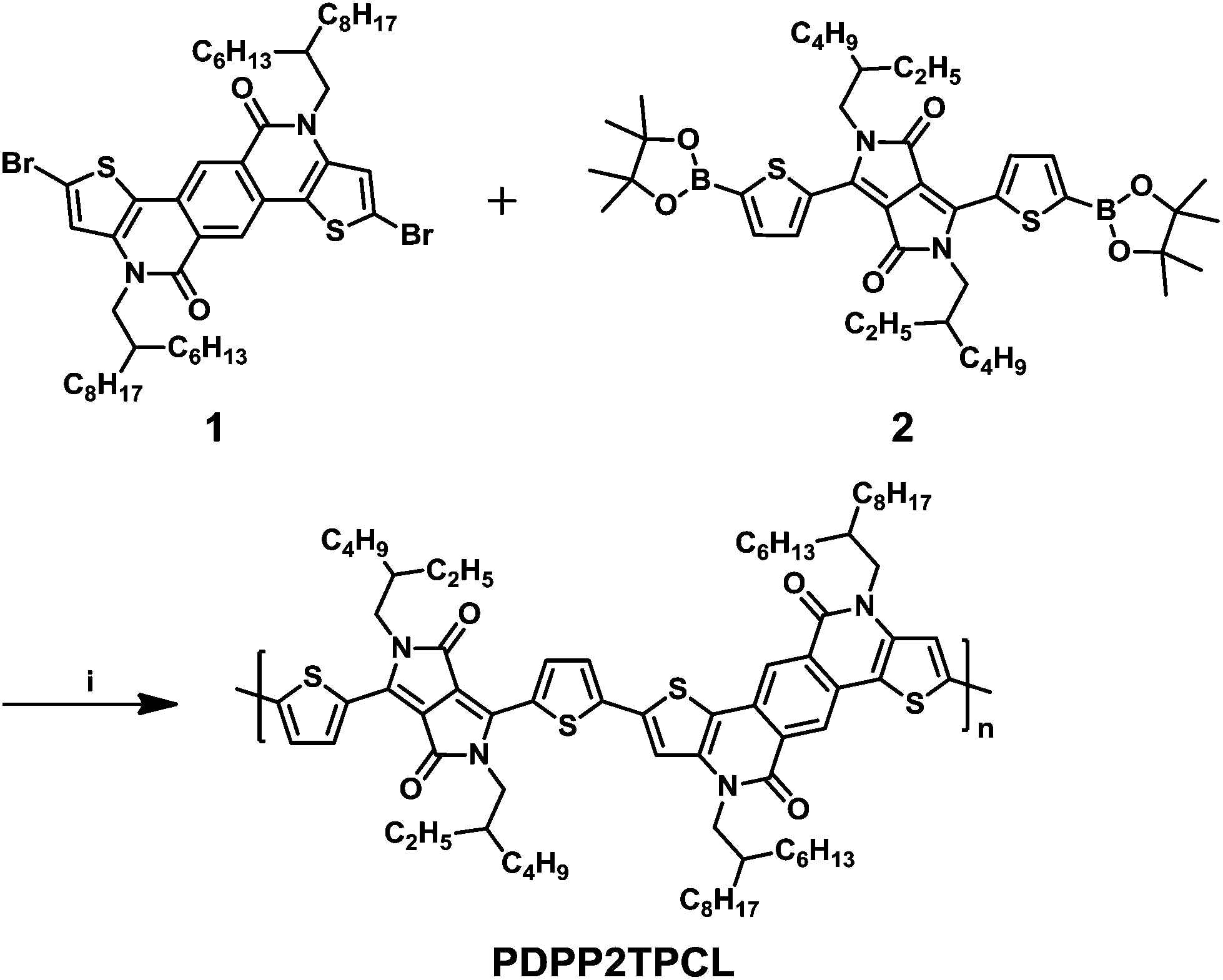 | ||
| Scheme 1 Chemical structure of the DPP polymer PDPP2TPCL and its synthetic route. (i) Suzuki polymerization using Pd2dba3/(t-Bu)3PH[BF4]/K3PO4 (aq)/Aliquat 336 in THF at 80 °C. | ||
Experimental
Materials and measurements
All synthetic procedures were performed under an argon atmosphere. The commercial chemicals were used as received. THF and toluene were distilled over sodium under an N2 atmosphere. [6,6]-Phenyl-C61-butyric acid methyl ester ([60]PCBM) was purchased from Solarmer Materials Inc. 2,8-Dibromo-4,10-bis(2-hexyldecyl)-4,10-dihydrothieno[2′,3′:5,6]pyrido[3,4-g]thieno[3,2-c]isoquinoline-5,11-dione (1)21 and 2,5-bis(2-ethylhexyl)-3,6-bis(5-(4,4,5,5-tetramethyl-1,3,2-dioxaborolan-2-yl)thiophen-2-yl)-2,5-dihydropyrrolo[3,4-c]pyrrole-1,4-dione (2)46 were synthesized according to literature procedures.1H-NMR and 13C-NMR spectra were recorded at 400 MHz and 100 MHz, respectively, on a Bruker AVANCE spectrometer with CDCl3 as the solvent and tetramethylsilane (TMS) as the internal standard. The molecular weight was determined with GPC at 140 °C on a PL-GPC 220 system using a PL-GEL 10 μm MIXED-B column and o-DCB as the eluent against polystyrene standards. A low concentration of 0.1 mg mL−1 of polymer in o-DCB was used to reduce aggregation. Electronic spectra were recorded on a JASCO V-570 spectrometer. Cyclic voltammetry was conducted with a scan rate of 0.1 V s−1 under an inert atmosphere with 1 M tetrabutylammonium hexafluorophosphate in o-DCB as the electrolyte. The working, counter and reference electrodes were glassy carbon, Pt wire and Ag/AgCl, respectively. The concentration of the sample in the electrolyte was approximately 1 mM, based on the monomers. All potentials were corrected against Fc/Fc+. Density functional theory (DFT) calculations were performed at the B3LYP/6-31G* level of theory using the Gaussian 09 program package. AFM images were recorded using a digital instruments nanoscope IIIa multimode atomic force microscope in tapping mode. Bright field TEM images were collected on a Hitachi SU8200 scanning electron microscope. Grazing-incidence wide-angle X-ray scattering (GIWAXS) measurements were conducted on a Xenocs-SAXS/WAXS system with an X-ray wavelength of 1.5418 Å. The film samples were irradiated at a fixed angle of 0.2°. All film samples were prepared by spin coating solutions on a Si/SiO2 substrate.
The organic field-effect transistors were fabricated on a commercial Si/SiO2/Au substrate purchased from First MEMS Co. Ltd. A heavily N-doped Si wafer with a SiO2 layer of 300 nm served as the gate electrode and dielectric layer, respectively. The Ti (2 nm)/Au (28 nm) source–drain electrodes were sputtered and patterned by a lift-off technique. Before deposition of the organic semiconductor, the gate dielectrics were treated with octadecyltrichlorosilane (OTS) in a vacuum oven at a temperature of 120 °C, forming an OTS self-assembled monolayer. The treated substrates were rinsed successively with hexane, chloroform (CHCl3), and isopropyl alcohol. Polymer thin films were spin coated on the substrate from solution with a thickness of around 30–50 nm. The polymer thin films were solution-processed from CHCl3 solution at room temperature, while the toluene solution with or without DPE as an additive was heated to 90 °C for hot spin coating. The devices were thermally annealed at 120 °C on a hotplate for 10 min in a glovebox filled with N2. The devices were assessed on a Keithley 4200 SCS semiconductor parameter analyzer at room temperature. The mobilities were calculated from the saturation region using the following equation: IDS = (W/2L)Ciμ(VG − VT)2, where IDS is the drain–source current, W is the channel width (1400 μm), L is the channel length (50 μm), μ is the field-effect mobility, Ci is the capacitance per unit area of the gate dielectric layer, and VG and VT are the gate voltage and threshold voltage, respectively. This equation defines the important characteristics of the electron mobility (μ), on/off ratio (Ion/Ioff), and threshold voltage (VT), which could be deduced by the equation from the plot of current–voltage.
Photovoltaic devices with an inverted configuration were made by spin coating a ZnO sol–gel47 at 4000 rpm for 60 s onto pre-cleaned, patterned ITO substrates. The photoactive layer was deposited by spin coating a chloroform (or toluene) solution containing the DPP polymers, [60]PCBM and an appropriate amount of a processing additive such as DIO, o-DCB, or DPE in air. The toluene solution was heated to 90 °C for hot spin coating. MoO3 (10 nm) and Ag (100 nm) were deposited by vacuum evaporation at ca. 4 × 10⁻⁵ Pa for the back electrode.
The active area of the cells was 0.04 cm2. The J–V characteristics were measured by a Keithley 2400 source meter unit under an AM1.5 G spectrum from a solar simulator (Enlitech model SS-F5-3A). The solar simulator illumination intensity was determined at 100 mW cm−2 using a monocrystal silicon reference cell with a KG5 filter. Short circuit currents under AM1.5 G conditions were estimated from the spectral response and convolution with the solar spectrum. The external quantum efficiency was measured by a Solar Cell Spectral Response Measurement System QE-R3011 (Enli Technology Co., Ltd). The thickness of the active layers in the photovoltaic devices was measured on a Veeco Dektak XT profilometer.
PDPP2TPCL
To a degassed solution of monomer 1 (88.72 mg, 95.3 μmol) and monomer 2 (74.01 mg, 95.3 μmol) in THF (4 mL) and H2O (1 mL) containing 2 M K3PO4, tris(dibenzylideneacetone)dipalladium(0) (2.62 mg, 2.86 μmol) and tri-tert-butylphosphonium tetrafluoroborate (3.32 mg, 11.4 μmol) were added. The mixture was stirred at 80 °C overnight, after which it was precipitated in methanol and filtered through a Soxhlet thimble. The polymer was extracted with acetone, hexane and chloroform. The chloroform fraction was reduced and the polymer was precipitated in acetone. The polymer was collected by filtering through a 0.45 μm PTFE membrane filter and dried in a vacuum oven to yield PDPP2TPCL (116.3 mg, 94%) as a dark solid. GPC (o-DCB, 140 °C): Mn = 72.8 kg mol−1, Mw = 239.9 kg mol−1 and PDI = 3.3.Results and discussion
Synthesis
The synthesis procedure for the polymer PDPP2TPCL is shown in Scheme 1. The monomers 2,8-dibromo-4,10-bis(2-hexyldecyl)-4,10-dihydrothieno[2′,3′:5,6]pyrido[3,4-g]thieno[3,2-c]isoquinoline-5,11-dione (1) and 2,5-bis(2-ethylhexyl)-3,6-bis(5-(4,4,5,5-tetramethyl-1,3,2-dioxaborolan-2-yl)thiophen-2-yl)-2,5-dihydropyrrolo[3,4-c]pyrrole-1,4-dione (2) were used to synthesise PDPP2TPCL via a Suzuki polymerization, where the Pd2dba3 catalyst and tri-tert-butylphosphonium tetrafluoroborate ((t-Bu)3PH[BF4]) ligand were applied to achieve a high molecular weight. The new polymer shows good solubility in chloroform (CHCl3) at room temperature, and can be dissolved in dichlorobenzene (o-DCB) or toluene at 90 °C. After cooling to room temperature, the polymer solution in toluene formed a gel-like structure in 2 min. The molecular weight of the polymer was determined by gel permeation chromatography (GPC) with o-DCB as the eluent at 140 °C, as shown in Fig. S1, ESI.† PDPP2TPCL shows a high number molecular weight (Mn) of 72.8 kg mol−1 and a PDI of 3.3, which is comparable to other DPP polymers.48Optical and electrochemical properties
UV-vis absorption spectra of the polymer PDPP2TPCL in CHCl3 and as a thin film are presented in Fig. 1a. The polymer shows an absorption peak at ≈760 nm with an onset at 847 nm. Compared to the dilute solution, the polymer shows a bathochromic shift absorption in the solid-state film as a result of aggregation. The optical band gap of PDPP2TPCL is 1.42 eV, determined by the absorption onset at 873 nm in the thin film.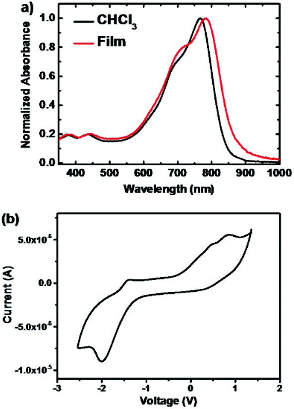 | ||
| Fig. 1 (a) Optical absorption spectra of PDPP2TPCL in CHCl3 solution (black line) and in the solid-state as a film (red line). (b) Cyclic voltammogram of the PDPP2TPCL thin film. Potential vs. Fc/Fc+. | ||
The HOMO and LUMO energy levels of PDPP2TPCL were determined by cyclic voltammetry (CV) measurements and are referenced to a work function of ferrocene of −5.23 eV (Fig. 1b). The polymer shows LUMO and HOMO levels of −3.89 eV and −5.06 eV, which provides a LUMO offset of 0.27 eV between the polymer and PCBM.49 This offset is close to 0.30 eV, which is generally accepted as the minimum driving force for efficient exciton separation into free charges.50 Recently, some research revealed that charge separation also occurs when the LUMO offset is below 0.30 eV,51,52 indicating that PDPP2TPCL can be potentially used as an electron donor for PSCs.
DFT-calculated molecular geometries and orbitals
To study the effect of the electron-deficient PCL and DPP units on the frontier orbitals over the conjugated backbone, density functional theory (DFT) calculations were carried out on oligomer PCL–TDPPT–PCL–TDPPT (Fig. 2). The polymer exhibits a coplanar backbone with very small torsion angles, which is helpful for forming crystalline structures in polymer thin films (Fig. 2a and b). The polymer has more localized HOMO and LUMO levels on the DPP segments, which indicates that the strong electron-deficient DPP units have a greater impact on the energy levels of the polymer (Fig. 2c and d). The high molecular weight, narrow band gap and coplanar backbone are beneficial for charge transport in FETs and PSCs.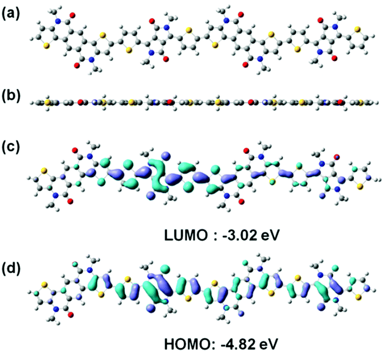 | ||
| Fig. 2 DFT calculations of the PCL–TDPPT–PCL–TDPPT segment. (a) Front view and (b) side view of the optimized molecular geometry. (c) and (d) Frontier molecular orbitals. | ||
Charge carrier mobility
The polymer PDPP2TPCL was applied in FETs with a BGBC configuration. The silicon dioxide gate dielectric used was passivated with octadecyltrichlorosilane (OTS). The polymer thin films were solution-processed from CHCl3 or toluene without or with DPE as an additive and thermally annealed for 10 min at 120 °C before the measurements were carried out. The FET devices from the polymer thin films without or with thermal annealing at 100 °C or 150 °C (Table S1†) showed low hole mobilities compared to the films thermally annealed at 120 °C (Table 1).| Solvent | μ h [cm2 V−1 s−1] | V T [V] | I on/Ioff |
|---|---|---|---|
| CHCl3 | 0.48 | −7.1 | 1 × 10⁴ |
| Toluene | 0.35 | −9.6 | 1 × 10⁴ |
| Toluene/DPE (2%) | 0.81 | −7.6 | 7 × 10⁴ |
The hole mobility of the polymer spin coated from CHCl3 solution was measured to be 0.48 cm2 V−1 s−1 (Fig. S2a and b, ESI,†Table 1). When the polymer thin film was spin coated from toluene solution, the hole mobility was slightly decreased to 0.35 cm2 V−1 s−1 (Fig. S2c and d, ESI,†Table 1). The hole mobility increased to 0.81 cm2 V−1 s−1 after adding high boiling point DPE as an additive into the polymer solution in toluene. FET devices fabricated from these solutions provided similar threshold voltages (VT) and on/off ratios (Table 1).
The difference in the hole mobilities of PDPP2TPCL spin coated from different solvents was further analyzed by atomic force microscopy (AFM) (Fig. 3c and d, Fig. S3, ESI†). The AFM images clearly show the fibril-like structures in these thin films, indicating the strong crystalline properties of PDPP2TPCL. In addition, the polymer thin films processed from toluene/DPE show a larger crystal domain than those from CHCl3 and toluene, which is further confirmed by their high roughness (3.02 nm) compared to the thin films from CHCl3 and toluene (0.87 nm and 0.88 nm) (Fig. S3, ESI†).
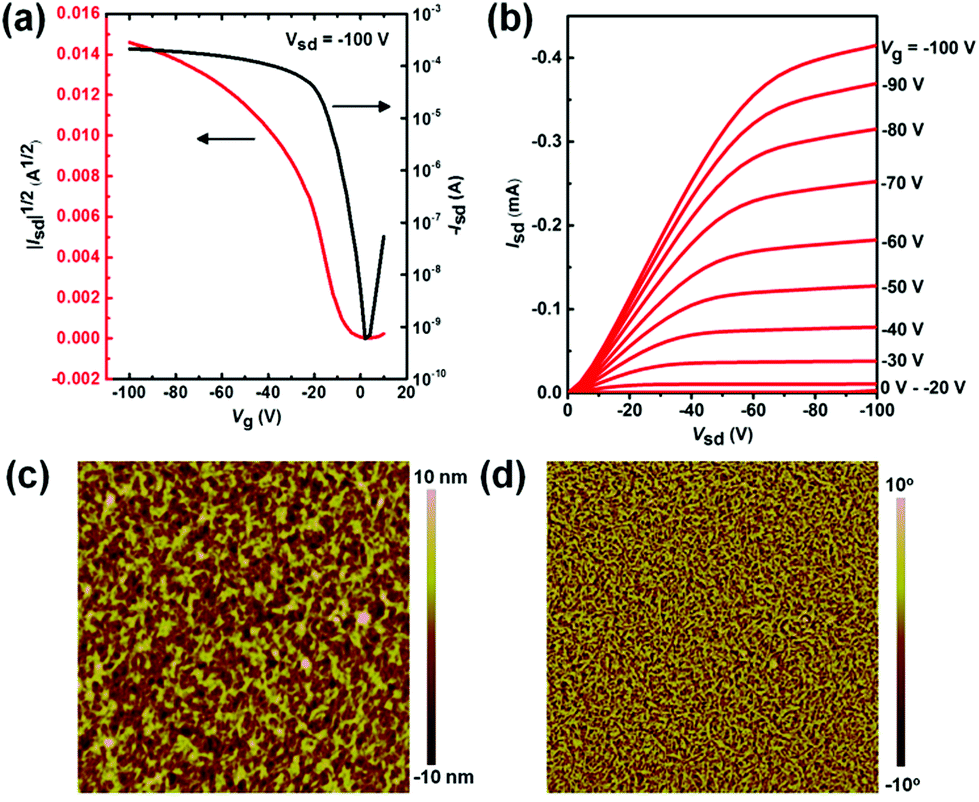 | ||
| Fig. 3 (a) Transfer and (b) output curves obtained from a BGBC FET device with a PDPP2TPCL thin film processed from toluene/DPE solution and annealed at 120 °C. (c) AFM height image (3 × 3 μm2) and (d) phase image of the corresponding thin film. The root mean square (RMS) roughness is 3.02 nm. | ||
It is interesting to mention that the electron mobilities are too low to be observed in these BGBC FET devices, even though the polymer PDPP2TPCL has a LUMO level of −3.89 eV. We further applied the top gate–bottom contact (TGBC) configuration with polymethylmethacrylate (PMMA) as the dielectric layer to fabricate PDPP2TPCL-based transistors (see ESI† for detailed experimental procedures). The electron mobilities were much lower than the hole mobilities (Fig. S4 and Table S2, ESI†). The low electron mobilities of the polymer PDPP2TPCL are probably due to the relatively high-lying LUMO level, the aggregation of the polymer thin films and environmental influences such as H2O and O2.
Photovoltaic properties
The polymer PDPP2TPCL was further applied as an electron donor in bulk-heterojunction photovoltaic cells by blending with phenyl-C61-butyric acid methyl ester ([60]PCBM) as an electron acceptor in an inverted device configuration with an ITO/ZnO electrode for electron collection and a MoO3/Ag electrode for hole collection. The photoactive layers were carefully optimized with respect to the solution processing solvent, the high boiling point additive, the donor to acceptor ratio and the thickness of the active layers (Tables S3–S5, Fig. S5–S7, ESI†). The optimized polymer![[thin space (1/6-em)]](https://www.rsc.org/images/entities/char_2009.gif) :PCBM weight ratio is 1:3. The J–V characteristics and external quantum efficiency (EQE) for the optimized solar cells are shown in Fig. 4 and Table 2. The short circuit current density (Jsc) was determined by integrating the EQE with the AM1.5 G spectrum.
:PCBM weight ratio is 1:3. The J–V characteristics and external quantum efficiency (EQE) for the optimized solar cells are shown in Fig. 4 and Table 2. The short circuit current density (Jsc) was determined by integrating the EQE with the AM1.5 G spectrum.
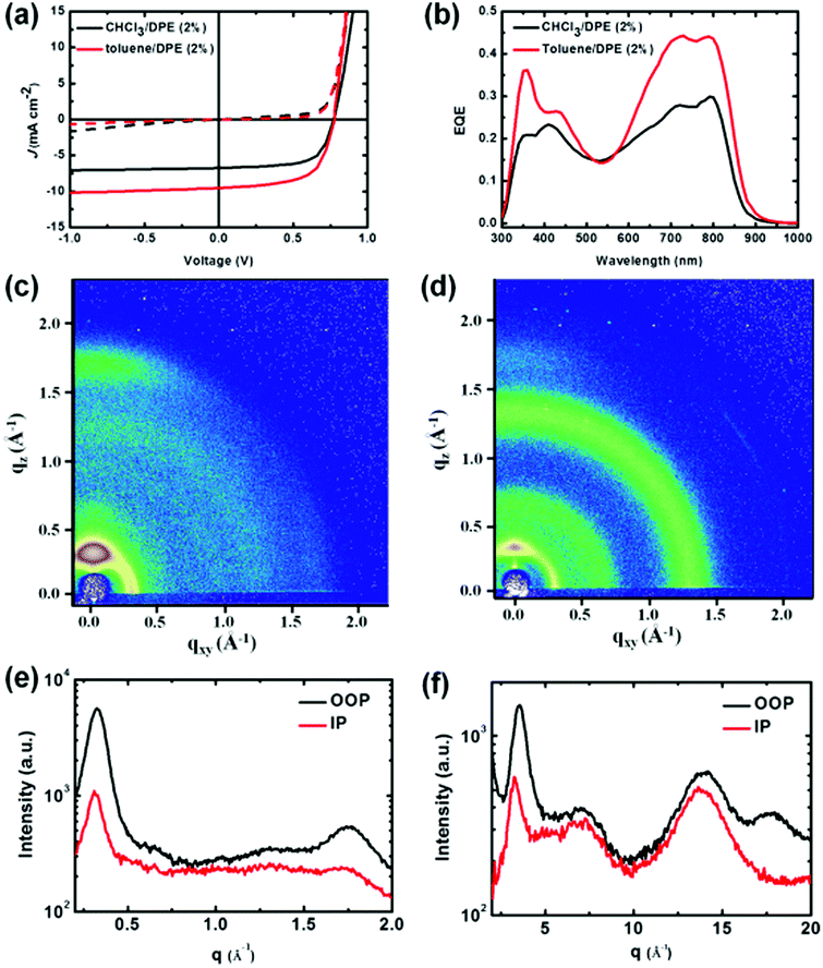 | ||
| Fig. 4 (a) J–V characteristics in the dark (dashed lines) and under white light illumination (solid lines). (b) EQE of the optimized polymer:[60]PCBM (1:3) inverted solar cells fabricated from CHCl3/DPE or toluene/DPE solutions. 2D-GIWAXS patterns of the thin films spin coated from toluene/DPE (2%): (c) PDPP2TPCL and (d) PDPP2TPCL:[60]PCBM (1:3). The out-of-plane (OOP) and in plane (IP) cuts of the corresponding 2D-GIWAXS patterns: (e) PDPP2TPCL and (f) PDPP2TPCL:[60]PCBM. | ||
:[60]PCBM (1:3)
Initially, the PDPP2TPCL:PCBM cells have a PCE of 3.4% with Jsc = 6.7 mA cm−2, an open circuit voltage (Voc) of 0.77 V and a high fill factor (FF) of 0.66 when the active layers were spin coated from CHCl3 with 2% DPE as an additive (Table 2). The PCE of the PDPP2TPCL:PCBM cells was dramatically increased to 4.7% when using toluene with 2% DPE as an additive, which is mainly due to the high Jsc value of 9.5 mA cm−2. These two cells show a broad photoresponse from 300 nm to 900 nm (Fig. 4b). The cells processed from CHCl3/DPE provide the maximum external quantum efficiency (EQE) of 0.30 at 795 nm, whereas the EQE of the cells from toluene/DPE increases to 0.44. The high EQE also explains the increased Jsc value. It is also noted that the energy loss of the PDPP2TPCL:PCBM cells, defined as the difference between the optical band gap and Voc, is 0.65 eV, which is close to the onset of 0.6 eV.51 The low energy loss, which is used to enhance the performance of photovoltaic devices, can be realized via deep LUMO levels of the donor polymers. Therefore, acceptor–acceptor polymers with low-lying LUMO levels have the potential to achieve high performance PSCs.
The photoactive layers were further studied by 2D-GIWAXS, AFM and TEM images (Fig. 4c–f and Fig. 5). PDPP2TPCL exhibits both (100) and (010) diffraction peaks in the out-of-plane direction, indicating that the PDPP2TPCL polymer chains on the surface have no clear preference for “edge on” or “face on” orientation. The (100) diffraction peaks in the PDPP2TPCL thin film with q = 0.32 Å−1 correlate to a lamellar distance of d = 19.63 nm (Table 3), which is attributed to the stacking alkyl side chains of the polymer. The distinct (010) diffraction peak of PDPP2TPCL in the out-of-plane direction proves π–π stacking (spacing: ≈3.61 Å). When PDPP2TPCL is blended with PCBM, (100) and (010) diffraction peaks in the out-of-plane direction are observed. Interestingly, the lamellar and π–π spacing are reduced to 17.95 Å and 3.51 Å respectively (Table 3), indicating that the polymer in PDPP2TPCL:PCBM blend thin films has highly dense molecular packing.
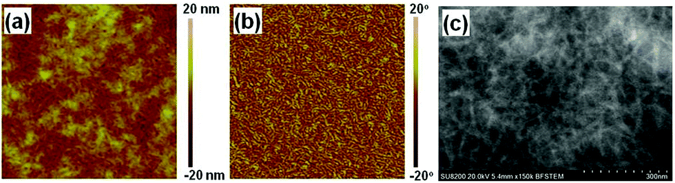 | ||
| Fig. 5 (a) AFM height (3 × 3 μm2), (b) phase and (c) TEM image of optimized PDPP2TPCL:[60]PCBM (1:3) spin coated from toluene/DPE (2%). The RMS roughness is 2.24 nm. | ||
| Lamellar spacing | π–π spacing | |||
|---|---|---|---|---|
| Q [Å−1] | D [Å] | Q [Å−1] | D [Å] | |
|
a From the GIWAXS patterns of the polymer:[60]PCBM films, the crystallographic parameters of [60]PCBM can also be calculated: q = 1.4 Å−1 and d = 4.49 Å. The polymer thin films were fabricated from toluene/DPE (2%) solutions.
|
||||
| PDPP2TPCL | 0.32 | 19.63 | 1.74 | 3.61 |
| PDPP2TPCL:[60]PCBMa |
0.35 | 17.95 | 1.79 | 3.51 |
The semi-crystalline properties of the PDPP2TPCL-based thin films can also be observed in the AFM and TEM images. As shown in the AFM images (Fig. 5a and b), the PDPP2TPCL:PCBM thin film solution processed from toluene/DPE clearly shows the fibrillar network. TEM images of the same thin films confirm that PDPP2TPCL presents fibril-like nanostructures with a diameter of 10–20 nm, which provide separated channels for charge transportation to the electrode. It is also noted that the diameter of the fibrils is slightly larger than those of efficient DPP polymer–fullerene blend films (<10 nm),53 which would reduce the photocurrent and PCE by preventing exciton diffusion into the donor/acceptor interface to generate charges.
Conclusions
A new conjugated polymer based on two electron-deficient units of PCL and DPP was designed, synthesized and applied in FETs and PSCs. The polymer has a high molecular weight, good solubility in toluene and a narrow band gap of 1.42 eV. FETs based on the polymer thin film solution processed from toluene with DPE as an additive have a hole mobility of 0.81 cm2 V−1 s−1. With the same solvent, PSCs based on the polymer provide a PCE of 4.7% with a photoresponse up to 900 nm and a low energy loss of 0.65 eV. The results demonstrate that acceptor–acceptor conjugated polymers can be used as electron donors in efficient FET and photovoltaic devices.Acknowledgements
We thank Ralf Bovee and Qiang Wang at Eindhoven University of Technology (TU/e, Netherlands) for the GPC analysis. This work was supported by the Recruitment Program of Global Youth Experts of China. The work was further supported by the National Natural Science Foundation of China (21574138).Notes and references
- P. Sonar, S. P. Singh, Y. Li, M. S. Soh and A. Dodabalapur, Adv. Mater., 2010, 22, 5409–5413 CrossRef CAS PubMed.
- S. Cho, J. Lee, M. H. Tong, J. H. Seo and C. Yang, Adv. Funct. Mater., 2011, 21, 1910–1916 CrossRef CAS.
- J. D. Yuen, J. Fan, J. Seifter, B. Lim, R. Hufschmid, A. J. Heeger and F. Wudl, J. Am. Chem. Soc., 2011, 133, 20799–20807 CrossRef CAS PubMed.
- P. Wang, H. Li, C. Gu, H. Dong, Z. Xu and H. Fu, RSC Adv., 2015, 5, 19520–19527 RSC.
- J.-K. Lee, M. C. Gwinner, R. Berger, C. Newby, R. Zentel, R. H. Friend, H. Sirringhaus and C. K. Ober, J. Am. Chem. Soc., 2011, 133, 9949–9951 CrossRef CAS PubMed.
- M. C. Gwinner, T. J. K. Brenner, J.-K. Lee, C. Newby, C. K. Ober, C. R. McNeill and H. Sirringhaus, J. Mater. Chem., 2012, 22, 4436–4439 RSC.
- J. Lee, S. Cho, J. H. Seo, P. Anant, J. Jacob and C. Yang, J. Mater. Chem., 2012, 22, 1504–1510 RSC.
- F. Grenier, P. Berrouard, J.-R. Pouliot, H.-R. Tseng, A. J. Heeger and M. Leclerc, Polym. Chem., 2013, 4, 1836–1841 RSC.
- G. Kim, A. R. Han, H. R. Lee, J. Lee, J. H. Oh and C. Yang, Chem. Commun., 2014, 50, 2180–2183 RSC.
- C. Ge, C. Mei, J. Ling, F. Zhao, H. Li, L. Liang, J. Wang, J. Yu, W. Shao, Y. Xie and W. Li, J. Polym. Sci., Part A: Polym. Chem., 2014, 52, 2356–2366 CrossRef CAS.
- K. Mahmood, H. Lu, Z.-P. Liu, C. Li, Z. Lu, X. Liu, T. Fang, Q. Peng, G. Li, L. Li and Z. Bo, Polym. Chem., 2014, 5, 5037–5045 RSC.
- K. H. Hendriks, G. H. L. Heintges, M. M. Wienk and R. A. J. Janssen, J. Mater. Chem. A, 2014, 2, 17899–17905 CAS.
- C. Ge, C. Mei, J. Ling, J. Wang, F. Zhao, L. Liang, H. Li, Y. Xie and W. Li, J. Polym. Sci., Part A: Polym. Chem., 2014, 52, 1200–1215 CrossRef CAS.
- A. Zhang, C. Xiao, D. Meng, Q. Wang, X. Zhang, W. Hu, X. Zhan, Z. Wang, R. A. J. Janssen and W. Li, J. Mater. Chem. C, 2015, 3, 8255–8261 RSC.
- I. H. Jung, W.-Y. Lo, J. Jang, W. Chen, D. Zhao, E. S. Landry, L. Lu, D. V. Talapin and L. Yu, Chem. Mater., 2014, 26, 3450–3459 CrossRef CAS.
- I. H. Jung, D. Zhao, J. Jang, W. Chen, E. S. Landry, L. Lu, D. V. Talapin and L. Yu, Chem. Mater., 2015, 27, 5941–5948 CrossRef CAS.
- M. Svensson, F. L. Zhang, S. C. Veenstra, W. J. H. Verhees, J. C. Hummelen, J. M. Kroon, O. Inganäs and M. R. Andersson, Adv. Mater., 2003, 15, 988–991 CrossRef CAS.
- Y. J. Cheng, S. H. Yang and C. S. Hsu, Chem. Rev., 2009, 109, 5868–5923 CrossRef CAS PubMed.
- H. Sirringhaus, Adv. Mater., 2014, 26, 1319–1335 CrossRef CAS PubMed.
- L. Dou, Y. Liu, Z. Hong, G. Li and Y. Yang, Chem. Rev., 2015 DOI:10.1021/acs.chemrev.5b00165.
- A. Facchetti, Mater. Today, 2013, 16, 123–132 CrossRef CAS.
- J. Cao, Q. Liao, X. Du, J. Chen, Z. Xiao, Q. Zuo and L. Ding, Energy Environ. Sci., 2013, 6, 3224–3228 CAS.
- Q. Liao, J. Cao, Z. Xiao, J. Liao and L. Ding, Phys. Chem. Chem. Phys., 2013, 15, 19990–19993 RSC.
- C. Zuo, J. Cao and L. Ding, Macromol. Rapid Commun., 2014, 35, 1362–1366 CrossRef CAS PubMed.
- H. Li, J. Cao, Q. Zhou, L. Ding and J. Wang, Nano Energy, 2015, 15, 125–134 CrossRef CAS.
- Z. Yi, S. Wang and Y. Liu, Adv. Mater., 2015, 27, 3589–3606 CrossRef CAS PubMed.
- Y. Li, P. Sonar, L. Murphy and W. Hong, Energy Environ. Sci., 2013, 6, 1684–1710 CAS.
- S. Y. Qu and H. Tian, Chem. Commun., 2012, 48, 3039–3051 RSC.
- K. H. Hendriks, W. Li, M. M. Wienk and R. A. J. Janssen, J. Am. Chem. Soc., 2014, 136, 12130–12136 CrossRef CAS PubMed.
- P. Sonar, S. P. Singh, Y. N. Li, Z. E. Ooi, T. J. Ha, I. Wong, M. S. Soh and A. Dodabalapur, Energy Environ. Sci., 2011, 4, 2288–2296 CAS.
- H. J. Chen, Y. L. Guo, G. Yu, Y. Zhao, J. Zhang, D. Gao, H. T. Liu and Y. Q. Liu, Adv. Mater., 2012, 24, 4618–4622 CrossRef CAS PubMed.
- Y. Li, P. Sonar, S. P. Singh, Z. E. Ooi, E. S. H. Lek and M. Q. Y. Loh, Phys. Chem. Chem. Phys., 2012, 14, 7162–7169 RSC.
- I. Kang, H.-J. Yun, D. S. Chung, S.-K. Kwon and Y.-H. Kim, J. Am. Chem. Soc., 2013, 135, 14896–14899 CrossRef CAS PubMed.
- H. H. Choi, J. Y. Baek, E. Song, B. Kang, K. Cho, S.-K. Kwon and Y.-H. Kim, Adv. Mater., 2015, 27, 3626–3631 CrossRef CAS PubMed.
- J. Y. Back, H. Yu, I. Song, I. Kang, H. Ahn, T. J. Shin, S.-K. Kwon, J. H. Oh and Y.-H. Kim, Chem. Mater., 2015, 27, 1732–1739 CrossRef CAS.
- C. Xiao, G. Zhao, A. Zhang, W. Jiang, R. A. J. Janssen, W. Li, W. Hu and Z. Wang, Adv. Mater., 2015, 27, 4963–4968 CrossRef CAS PubMed.
- Z. Y. Chen, M. J. Lee, R. S. Ashraf, Y. Gu, S. Albert-Seifried, M. M. Nielsen, B. Schroeder, T. D. Anthopoulos, M. Heeney, I. McCulloch and H. Sirringhaus, Adv. Mater., 2012, 24, 647–652 CrossRef CAS PubMed.
- H.-J. Yun, S.-J. Kang, Y. Xu, S. O. Kim, Y.-H. Kim, Y.-Y. Noh and S.-K. Kwon, Adv. Mater., 2014, 26, 7300–7307 CrossRef CAS PubMed.
- B. Sun, W. Hong, Z. Yan, H. Aziz and Y. Li, Adv. Mater., 2014, 26, 2636–2642 CrossRef CAS PubMed.
- B. Sun, W. Hong, H. Aziz and Y. Li, Polym. Chem., 2015, 6, 938–945 RSC.
- J. H. Park, E. H. Jung, J. W. Jung and W. H. Jo, Adv. Mater., 2013, 25, 2583–2588 CrossRef CAS PubMed.
- T. Ma, K. Jiang, S. Chen, H. Hu, H. Lin, Z. Li, J. Zhao, Y. Liu, Y.-M. Chang, C.-C. Hsiao and H. Yan, Adv. Energy Mater., 2015 DOI:10.1002/aenm.201501282.
- H. Choi, S.-J. Ko, T. Kim, P.-O. Morin, B. Walker, B. H. Lee, M. Leclerc, J. Y. Kim and A. J. Heeger, Adv. Mater., 2015, 27, 3318–3324 CrossRef CAS PubMed.
- R. S. Ashraf, I. Meager, M. Nikolka, M. Kirkus, M. Planells, B. C. Schroeder, S. Holliday, M. Hurhangee, C. B. Nielsen, H. Sirringhaus and I. McCulloch, J. Am. Chem. Soc., 2015, 137, 1314–1321 CrossRef CAS PubMed.
- K. H. Hendriks, G. H. L. Heintges, V. S. Gevaerts, M. M. Wienk and R. A. J. Janssen, Angew. Chem., Int. Ed., 2013, 52, 8341–8344 CrossRef CAS PubMed.
- H. Bürckstümmer, A. Weissenstein, D. Bialas and F. Würthner, J. Org. Chem., 2011, 76, 2426–2432 CrossRef PubMed.
- Y. M. Sun, J. H. Seo, C. J. Takacs, J. Seifter and A. J. Heeger, Adv. Mater., 2011, 23, 1679–1683 CrossRef CAS PubMed.
- W. Li, K. H. Hendriks, A. Furlan, W. S. C. Roelofs, M. M. Wienk and R. A. J. Janssen, J. Am. Chem. Soc., 2013, 135, 18942–18948 CrossRef CAS PubMed.
- M. M. Wienk, J. M. Kroon, W. J. H. Verhees, J. Knol, J. C. Hummelen, P. A. van Hal and R. A. J. Janssen, Angew. Chem., Int. Ed., 2003, 42, 3371–3375 CrossRef CAS PubMed.
- C. J. Brabec, C. Winder, N. S. Sariciftci, J. C. Hummelen, A. Dhanabalan, P. A. van Hal and R. A. J. Janssen, Adv. Funct. Mater., 2002, 12, 709–712 CrossRef CAS.
- W. Li, K. H. Hendriks, A. Furlan, M. M. Wienk and R. A. J. Janssen, J. Am. Chem. Soc., 2015, 137, 2231–2234 CrossRef CAS PubMed.
- K. Gao, L. Li, T. Lai, L. Xiao, Y. Huang, F. Huang, J. Peng, Y. Cao, F. Liu, T. P. Russell, R. A. J. Janssen and X. Peng, J. Am. Chem. Soc., 2015, 137, 7282–7285 CrossRef CAS PubMed.
- W. Li, K. H. Hendriks, A. Furlan, W. S. C. Roelofs, S. C. J. Meskers, M. M. Wienk and R. A. J. Janssen, Adv. Mater., 2014, 26, 1565–1570 CrossRef CAS PubMed.
Footnote |
| † Electronic supplementary information (ESI) available. See DOI: 10.1039/c5py01406a |
| This journal is © The Royal Society of Chemistry 2016 |