
 Open Access Article
 This Open Access Article is licensed under a
 Creative Commons Attribution 3.0 Unported Licence
Tuning the electronic properties of transition-metal trichalcogenides via tensile strain†
Ming
Li
ab,
Jun
Dai
b and
Xiao Cheng
Zeng
*b
aCollege of Chemical engineering, North China University of Science and Technology, Tang shan, Hebei 063000, China
bDepartment of Chemistry and Department Mechanics and Materials Engineering, University of Nebraska-Lincoln, Lincoln, NE 68588, USA. E-mail: xzeng1@unl.edu
First published on 17th August 2015
Abstract
A comprehensive study of the effect of tensile strain (ε = 0% to 8%) on the electronic structures of two-dimensional (2D) transition-metal trichalcogenide (TMTC) monolayers MX3 (M = Ti, Zr, Hf, Nb; X = S, Se Te) is performed on the basis of density functional theory (DFT) computation. The unstrained TiS3, ZrS3, ZrSe3, HfS3, HfSe3 and NbS3 monolayers are predicted to be semiconductors with their bandgap ranging from 0.80 to 1.94 eV. Our DFT computations show that the biaxial and uniaxial tensile strains can effectively modify the bandgap of many TMTC monolayers. In particular, we find that ZrS3 and HfS3 monolayers undergo an indirect-to-direct bandgap transition with increasing tensile strain. The indirect bandgaps of ZrSe3 and HfSe3 monolayers also increase with the tensile strain. Both ZrTe3 and HfTe3 monolayers are predicted to be metals, but can be transformed into indirect bandgap semiconductors at ε = 4% and ε = 6%, respectively. Importantly, the TiS3 monolayer can retain its direct-bandgap feature over a range of biaxial or uniaxial tensile strains (up to 8%). The highly tunable direct bandgaps of MS3 (M = Hf, Ti, and Zr) by strain and the availability of metallic and semiconducting properties of MTe3 (M = Hf and Zr) provide exciting opportunities for designing artificial layered structures for applications in optoelectronics and flexible electronics.
Introduction
In recent years, 2D layered nanomaterials have attracted intensive interest due to their novel electronic, optical, thermal, and mechanical properties for potential applications in various fields. With regard to transition-metal based 2D materials, thus far, predominant investigations have been focused on the transition metal dichalcogenides (TMDCs) such as MoS2, not only because of their novel electronic and catalytic properties but also their high tunability via strain or a vertical electric field.1–6 Remarkably, large-scale growth of monolayered MoS2 films with spatial homogeneity and high electrical performance has been recently demonstrated in the laboratory.7 It has also been demonstrated that MoS2 exhibits many exotic characteristics that are absent in its bulk counterpart.8–10 MoS2 is a semiconductor with a direct bandgap, although the bulk MoS2 possesses an indirect bandgap.11 The direct bandgap character of 2D layered materials such as monolayered MoS2 is highly desired for applications in thinner transistors, thermoelectrics and solar cells. Towards this end, several new chemical approaches to contrive new 2D nanomaterials have been reported,12–14 which renders synthesis of new monolayered nanomaterials more accessible.Like TMDCs, many bulk transition metal trichalcogenides (TMTCs) exhibit layered structures with weak interlayer van der Waals interactions. Most TMTCs, i.e. MX3 (M = Ti, Zr, Hf; X = S, Se, Te), possess monoclinic crystalline structures with the space group P21/m,15,16 while the space group of NbS3 is P1 and its most stable crystalline structure is triclinic.17,18 Although many bulk MX3 compounds have been studied for several decades,19–26 2D MX3 layered materials have received little attention until very recently when the new monolayered TiS3 was isolated,27,28 and was also predicted to possess exciting electronic properties such as a direct band gap (1.06 eV) close to that of silicon.29 Note that the bulk TiS3 is an n-type semiconductor with an indirect band gap. Previous studies also showed that TiS3 possesses lower cleavage energy than graphite.29,30 Indeed, Island et al. demonstrated that a TiS3 film can be exfoliated down to single layers with high photoresponse and fast switching rates.31
As pointed out previously, 2D layered semiconducting materials with direct and tunable bandgaps are highly desired for nanoelectronic and optoelectronic applications.32–38 It is known that engineering 2D layered materials by strain is a viable approach to achieve tunable electronic properties.39–46 Over the past few years, effects of strains on electronic properties of TMDCs have been extensively studied, especially from the theoretical viewpoint.47–53 It was predicted that some TMDC monolayers can undergo an indirect-to-direct bandgap transition under the tensile strain. Hence, it is timely and important to explore whether the indirect-to-direct bandgap transition can occur when TMTC monolayers are under tensile strain. In this study, effects of both biaxial and uniaxial strains on the bandgap of a series of MX3 monolayers (M = Ti, Zr, Hf, Nb; X = S, Se, Te) are investigated. We find that as in the case of TMDCs, the tensile strains can strongly modify the bandgap of many TMTC monolayers.
Computational methods
All computations were performed within the framework of density functional theory (DFT), using the Vienna ab initio simulation package (VASP 5.3).54 The core–valence interaction was described by the projector augmented wave (PAW) method.55 The generalized gradient approximation (GGA) in the form of Becke86 was adopted for the exchange–correlation functional.56 More specifically, the optB86b-vdW functional, implemented to account for weak van der Waals (vdW) interactions,57 was used for structure optimization (we also examined two other GGA functionals with the vdW correction, namely optPBE-vdW and optB88-vdW, and found that the optB86b-vdW functional gives the best agreement with experiments in predicting the lattice constants of bulk TMTCs). It is known that GGA functionals tend to underestimate the band gap of semiconductors. So the electronic structures were computed using the Heyd–Scuseria–Ernzerhof (HSE06) hybrid functional.58 The same computations were also performed with the optB86-vdW functional to confirm the general trend of strain-dependent bandgaps. Energy cut off for the plane-wave expansion was set to 500 eV. Brillouin zone sampling was performed with Monkhorst–Pack (MP) special k-point meshes. The 2D Brillouin zone integration using the Γ-center scheme was sampled with a 7 × 10 × 1 grid for geometry optimizations (7 × 10 × 4 for bulk systems), and the k-point grid scaled with respect to the supercell size. A vacuum layer greater than 15 Å was taken to avoid interaction between adjacent images. All atoms were allowed to relax during the geometry optimization until the computed Hellmann–Feynman force on each atom was smaller than 0.02 eV Å−1. The convergence threshold was set as 10−4 eV in energy. Spin–orbit coupling (SOC) was included when computing the band structures. Tensile strain ranging from 0 to 8% was considered. The tensile strain was undertaken in three different ways: (1) biaxial expansion in both the x and y directions (xy), uniaxial expansion of the monolayer in the x direction (xx) or the y direction (yy).51 For the uniaxial strain, the Poisson effect is considered. The strain scale is defined as ε = Δm/m0. For biaxial tensile strain, m0 is the unstrained cell parameter, and Δm + m0 is the strained cell parameter. For uniaxial tensile strain, m0 is the projection of the unit-cell vector in the x or y direction, and Δm is the associated change from m0.Results and discussion
As mentioned above, the optimized lattice vectors based on the optB86b-vdW functional agree well with the experimental data. For example, the optimized lattice constants of ZrS3 bulk are a0 = 5.133 Å, b0 = 3.624 Å, c0 = 9.008 Å, and β = 97.15°, in good agreement with the experimental values (a0 = 5.124 Å, b0 = 3.624 Å, c0 = 8.980 Å, and β = 97.28°). Note that the TMTC bulks often have many allotropes.15–17 In this study, we only consider TMTC monolayers cleaved from the most stable bulk allotrope at 0 K. For TiX3, ZrX3, and HfX3, the most stable crystalline structure is monoclinic, while for NbS3 the most stable crystalline structure is triclinic. Next, the band structures of MX3 bulks are computed using the HSE06 functional. The HSE06 bandgaps of TiS3, ZrS3, ZrSe3, HfS3, HfSe3 and NbS3 bulks are 1.05 eV, 1.87 eV, 0.68 eV, 1.90 eV, 0.59 eV and 1.07 eV, respectively, in good agreement with the measured bandgaps from experiments.32–38 For example, the measured bandgap of ZrS3 and HfS3 is 1.91 and 1.95 eV, respectively.The optimized lattice constants of TMTC monolayers (see Fig. 1 for structures) based on the optB86b-vdW functional are summarized in Table 1, together with the computed HSE06 bandgaps. For the band-structure computation, the Brillouin zone of ΓYAΓB (Fig. 1c) is selected.
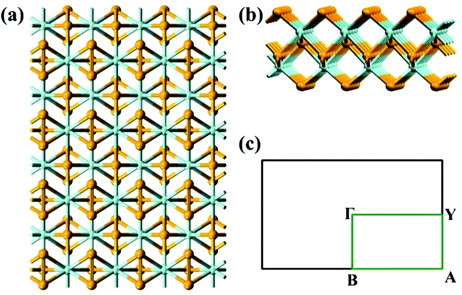 | ||
| Fig. 1 (a) Top view and (b) side view of a 4 × 4 MX3 monolayered sheet, (c) the first Brillouin zone and the high symmetry points associated with the MX3 monolayer. The ocher and cyan spheres refer to M and X atoms, respectively. | ||
| a 0 (Å) | b 0 (Å) | Bandgap (eV) | Direct/indirect | |
|---|---|---|---|---|
| ZrS3 | 5.138 | 3.619 | 1.92 | I |
| ZrSe3 | 5.423 | 3.745 | 0.92 | I |
| ZrTe3 | 5.942 | 3.909 | Metal | — |
| HfS3 | 5.092 | 3.576 | 1.94 | I |
| HfSe3 | 5.402 | 3.709 | 0.80 | I |
| HfTe3 | 5.941 | 3.882 | Metal | — |
| TiS3 | 4.970 | 3.386 | 1.08 | D |
| NbS3 | 4.992 | 6.746 | 1.18 | I |
As shown in Table 1, the unstained TiS3 monolayer is the only TMTC considered with a direct bandgap. Table 1 also shows that ZrS3, ZrSe3, HfS3, HfSe3, and NbS3 monolayers are also semiconductors but with an indirect bandgap. ZrTe3 and HfTe3 are predicted to have the electronic structures of metals. Previously, we have examined the dynamical stability of the TiS3 monolayer by computing its phonon spectrum.29 Here we have also computed the phonon spectrum of two prototype monolayers, HfS3 and HfSe3, one is the direct semiconductor under biaxial strain while another is the indirect semiconductor under all types of strain. As shown in ESI Fig. S1,† there is no negative frequency in the computed phonon spectrum of HfS3 and HfSe3 monolayers.
Next, the effect of tensile strain on the electronic structures of MX3 monolayers (M = Zr, Hf; X = S, Se Te) is investigated in detail. The computed HSE06 bandgaps of MX3 monolayers (M = Zr, Hf; X = S, Se Te), subjected to biaxial or uniaxial strain ranging from 0% to 8% are summarized in Fig. 2.
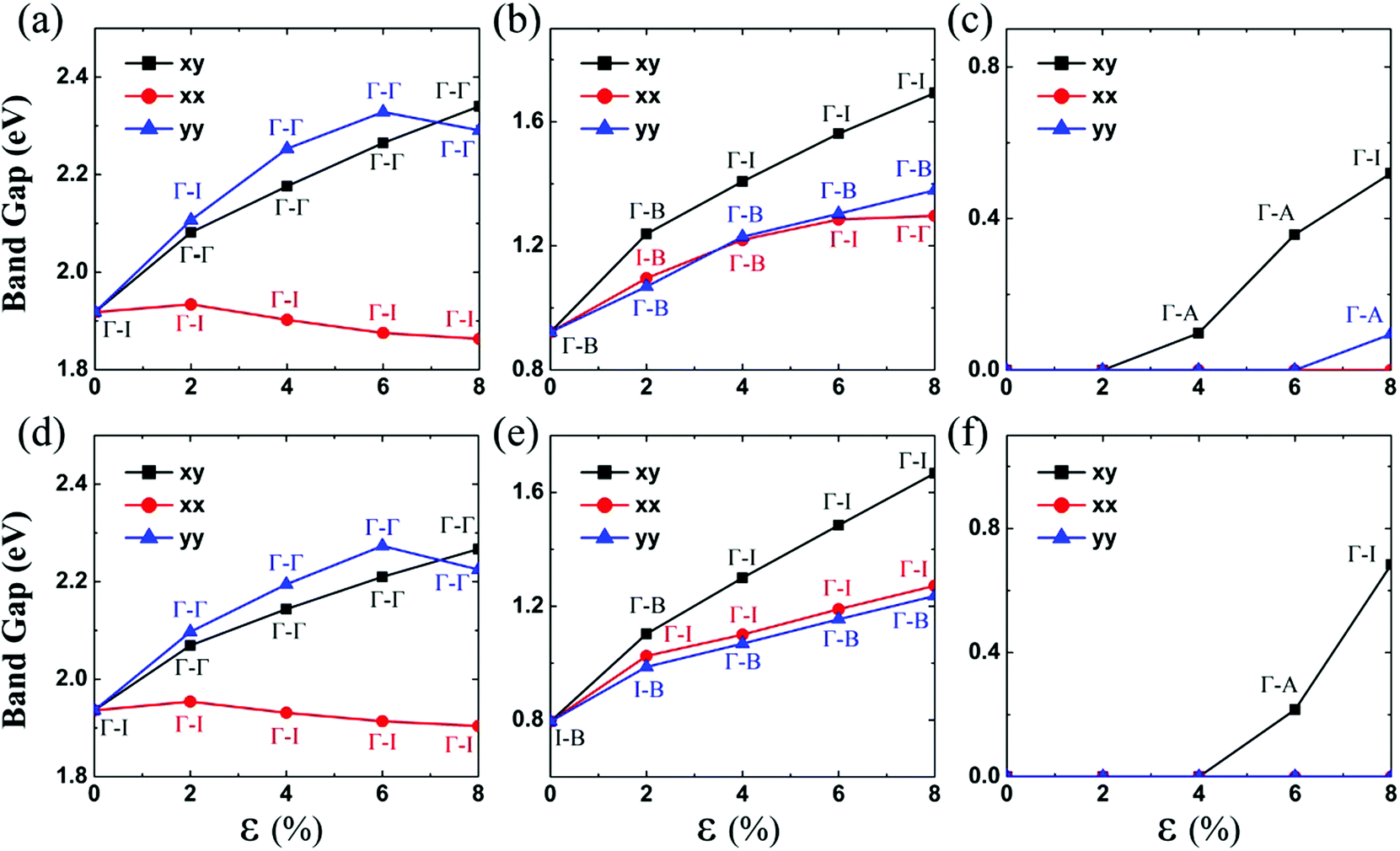 | ||
| Fig. 2 Computed bandgaps of (a) ZrS3, (b) ZrSe3, (c) ZrTe3, (d) HfS3, (e) HfSe3, and (f) HfTe3 monolayers versus the biaxial or uniaxial tensile strain, ranging from ε = 0% to 8%. The black lines denote the bandgap versus biaxial tensile strain in both the x and y directions. The red lines denote the bandgap versus the uniaxial tensile strain in the x direction, and the blue lines denote the bandgap versus the uniaxial tensile strain in the y direction. Γ, A and B represent the special points in the first Brillouin zone (Fig. 1(c)), while I refers to either the valence band maximum or conduction band minimum that is not located at the Γ point. Hence, Γ–Γ denotes the direct bandgap, whereas Γ–A, Γ–B and Γ–I denote the indirect bandgap. | ||
ZrX3 and HfX3
The unstrained ZrS3 monolayer is a semiconductor with an indirect bandgap of 1.92 eV. As shown in Fig. 3(a), the conduction band minimum (CBM) and valence band maximum (VBM) are located at Γ point and I point, respectively. Here, the energy at I point is only 0.07 eV higher than that at the Γ point. The CBM is mainly contributed by dz2 and dx2−y2 orbitals of the Zr atom, while the VBM is mainly contributed by px and py orbitals of the S atom. The partial density of states (PDOS) is depicted in ESI Fig. S2.†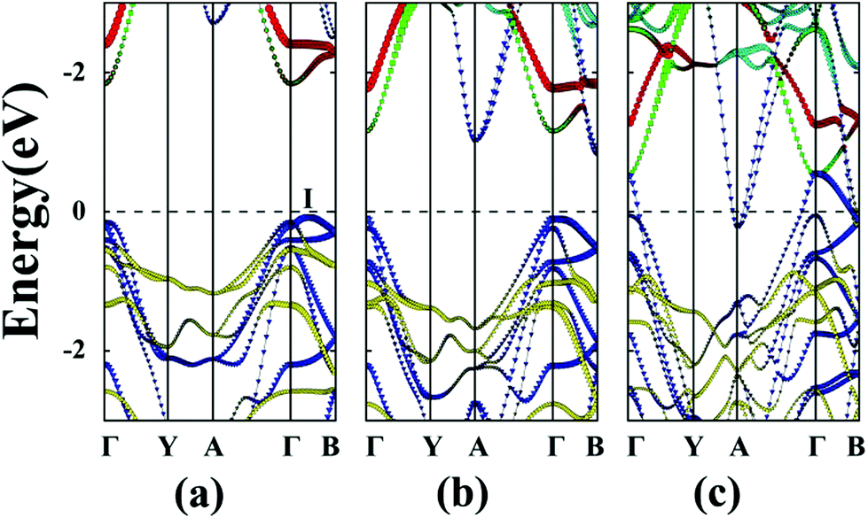 | ||
| Fig. 3 Band structures of unstrained monolayers (a) ZrS3, (b) ZrSe3, and (c) ZrTe3. The red lines denote the dz2 orbital of the Zr atom. The green lines denote the dx2−y2 orbitals of the Zr atom. The cyan lines denote the dxy, dyz and dxz orbitals of the Zr atom. The blue lines denote the px and py orbitals of (a) S, (b) Se, (c) and Te atoms, and the yellow lines denote the pz orbital of (a) S, (b) Se, and (c) Te atoms. The dashed lines indicate the Fermi level. The I point refers to the VBM not located at the Γ point. | ||
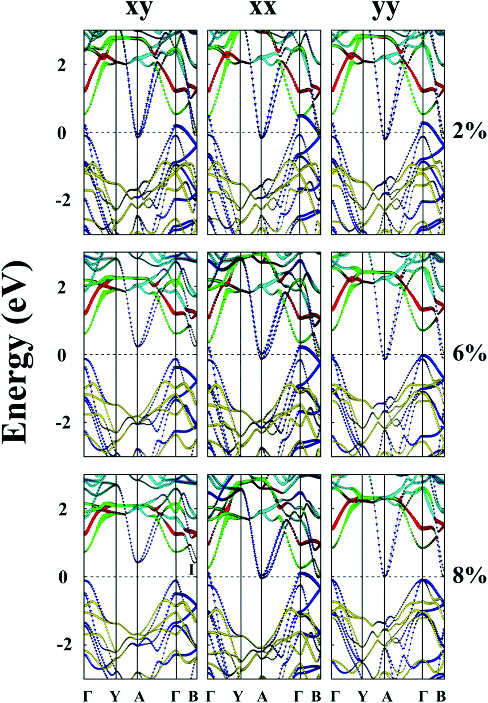
When the ZrS3 monolayer is subjected to the biaxial tensile strain of ε = 2% in both the x and y directions, its bandgap increases to 2.08 eV. More interestingly, as illustrated in Fig. 4, the ZrS3 monolayer transforms from an indirect to direct bandgap semiconductor, as both the VBM and CBM are located at the Γ point. This transformation is mainly due to the energy (of the p orbital of the S atom) at the Γ point shifting above the energy at I point, thereby the VBM is changed from I point to Γ point. The CBM however is still located at the Γ point, resulting in a direct bandgap. Moreover, upon increasing the biaxial strain to a high value of ε = 8%, the direct bandgap character is still retained although the bandgap is increased from 1.92 to 2.34 eV.
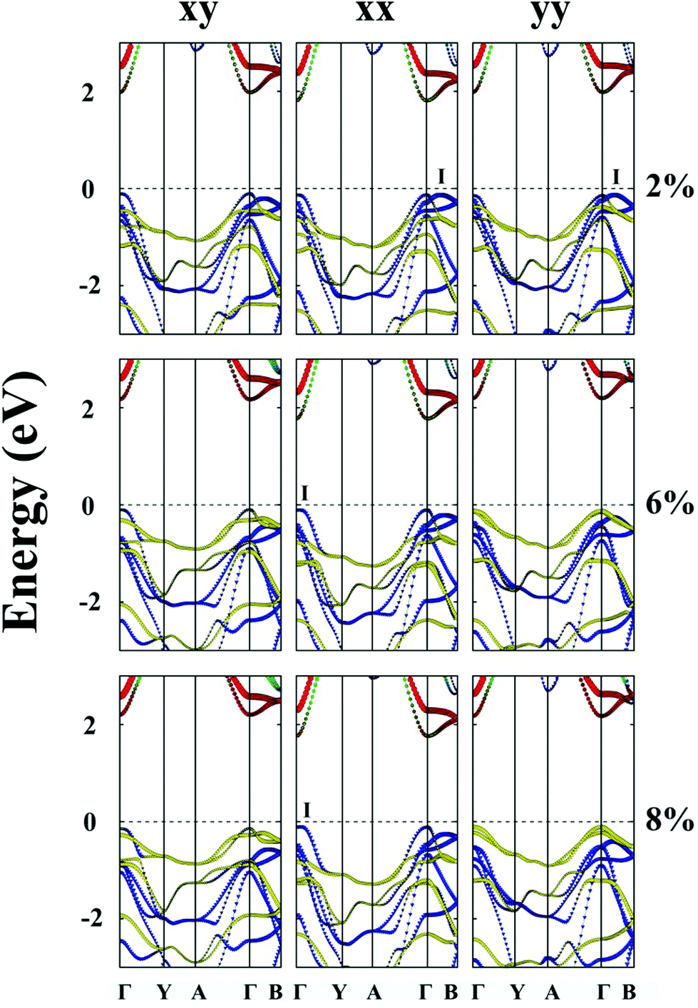 | ||
| Fig. 4 Computed band structures of strained monolayered ZrS3 under the biaxial tensile strain in both the x and y directions (xy), or under the uniaxial tensile strain in the x direction (xx) or the y direction (yy). The red and green lines illustrate the dz2 orbital and the dx2−y2 orbital of the Zr atom, respectively. The cyan lines denote the dxy, dyz and dxz orbitals of the Zr atom. The blue lines denote the px and py orbitals of the S atom, and the yellow lines denote the pz orbital of the S atom. The dashed lines indicate the Fermi level. The I point refers to the VBM not located at the Γ point. | ||
Likewise, the uniaxial tensile strain of ε = 4% along the y direction can also lead to the indirect-to-direct bandgap transition for the ZrS3 monolayer. The direct bandgap character is maintained even when the strain is as high as 8%. Meanwhile, the uniaxial expansion in the y direction initially increases the bandgap from 1.92 to 2.33 eV at ε = 6%, and then slightly reduces the bandgap to 2.29 eV at ε = 8%.
When the monolayered ZrS3 is subjected to uniaxial tensile strain in the x direction, as shown in Fig. 4, the indirect bandgap character is maintained even when the strain is as high as 8%. In addition, uniaxial expansion in the x direction only slightly changes the bandgap from 1.92 to 1.93 eV at ε = 2%, while it reduces the bandgap to 1.86 eV at ε = 8%.
Unstained monolayered ZrSe3 is a semiconductor with an indirect bandgap of 0.92 eV (Fig. 3(b)), and the VBM and CBM are located at the Γ and B points, respectively. Both VBM and CBM are mainly contributed by px and py orbitals of the Se atom. When the monolayered ZrSe3 is subjected to biaxial tensile strain from 2% to 8%, the bandgap increases from 1.24 to 1.69 eV (Fig. 2 and ESI Fig. S3†). The ZrSe3 monolayer remains an indirect bandgap semiconductor, as the VBM is always located at the Γ point, while the CBM shifts from B to I point at ε = 4%. As shown in ESI Fig. S3,† upon increasing the strain to ε = 8%, the CBM is still located at the I point.
Upon applying the uniaxial tensile strain of ε = 2% along the x direction to the monolayered ZrSe3, the VBM shifts from the Γ to the I point. Interestingly, at ε = 4%, the VBM shifts back to the Γ point. At ε = 8%, the energy (of the p orbital of the S atom) at the B point shifts above that at the Γ point. Consequently, the CBM shifts from the B point to the Γ point, whereas the VBM is still located at the Γ point, resulting in a direct bandgap. The uniaxial tensile strain in the x direction increases the bandgap from 1.10 to 1.30 eV at ε = 8%.
When the monolayered ZrSe3 is subjected to uniaxial tensile strain in the y direction, the VBM is always located at the Γ point, and the CBM is always located at the B point. In any event, the uniaxial expansion in the y direction can modulate the indirect bandgap from 1.07 to 1.38 eV.
For HfS3 and HfSe3 monolayers, the strain-dependent bandgap behavior is quite similar to that of ZrS3 and ZrSe3. The detailed electronic structure versus tensile strain for HfS3 and HfSe3 is shown in ESI Fig. S4–S6.†
Unlike MS3 and MSe3, unstrained ZrTe3 and HfTe3 monolayers are predicted to be metals. Importantly, when the ZrTe3 monolayer is subjected to biaxial tensile strain of ε = 4%, it transforms from a metal to semiconductor with an indirect bandgap of 0.10 eV. The VBM and CBM are located at the Γ point and A point, respectively. As shown in Fig. 5, the valence band near the Fermi level is mainly contributed by px and py orbitals of the Te atom, and the CBM is mainly contributed by the pz orbital of the Te atom. The energy splitting between the p orbital at Γ point and at A point increases with increasing the biaxial tensile strain, leading to the metal-to-semiconductor transition. At ε = 8% the CBM shifts from A to I point and the bandgap increases to 0.52 eV. Uniaxial expansion in the y direction to ε = 8% can open a bandgap of 0.10 eV. In contrast, upon applying uniaxial tensile strain along the x direction, the metallic character of the ZrTe3 monolayer is retained even at ε = 8%.
 | ||
| Fig. 5 Computed band structures of strained monolayered ZrTe3 under the biaxial tensile strain (xy) in both the x and y directions, or under the uniaxial tensile strain in the x direction (xx) or the y direction (yy). The red lines denote the dz2 orbital of the Zr atom. The green lines denote the dx2−y2 orbitals of the Zr atom. The cyan lines denote the dxy, dyz and dxz orbitals of the Zr atom. The blue lines denote the px and py orbitals of the Te atom, and the yellow lines denote the pz orbital of the Te atom. The dashed lines indicate the Fermi level. The I point refers to the CBM not located at the Γ point. | ||
Like ZrTe3, upon applying uniaxial tensile strain along the x direction, the metallic character of the HfTe3 monolayer is still retained, even at ε = 8% (ESI Fig. S7†). HfTe3 also keeps the metallic character even under uniaxial stain of ε = 8% in the y direction. Only the biaxial tensile strain can open a bandgap of HfTe3, e.g., to 0.22 eV at ε = 6% and to 0.68 eV at ε = 8%. At the two strains, the VBM is located at the Γ point while the CBM is located at the A point and I point, respectively.
TiS3 and NbS3
Lastly, the effect of tensile strain on the bandgap of the TiS3 monolayer is also investigated. The TiS3 monolayer is a semiconductor with a direct bandgap of 1.08 eV. As illustrated in Fig. 6(a) and 7 and ESI Fig. S8.† Both VBM and CBM are located at the Γ point, consistent with the results of previous studies.29 The bandgap can increase up to 1.37 eV at the biaxial tensile strain ε = 8%. Likewise, upon applying uniaxial strain along the y direction, the direct bandgap character is maintained even at ε = 8%, and the bandgap is enlarged from 1.21 to 1.60 eV. The latter is wider than the enlarged bandgap at the biaxial strain of ε = 8%. In contrast, when the monolayered TiS3 is subjected to uniaxial tensile strain in the x direction, although its direct gap character is maintained even at ε = 8%, the bandgap is actually reduced from 1.08 eV to 1.01 eV at ε = 2%, and to 0.91 eV at ε = 8%. The opposite trend of bandgap change is due to the downward shift of CBM at the Γ point. Here, the VBM is mainly contributed by px and py orbitals of the S atom, while the CBM is mainly contributed by dz2 and dx2−y2 orbitals of the Ti atom.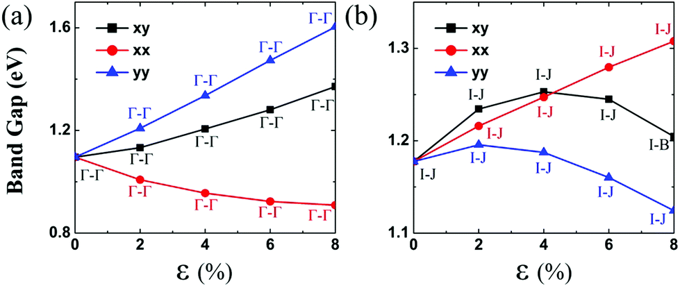 | ||
| Fig. 6 Bandgap of (a) TiS3 and (b) NbS3 monolayers versus the biaxial and uniaxial tensile strain ranging from 0% to 8%. The black lines denote the bandgap versus biaxial tensile strain both in the x and y directions. The red lines denote the bandgap versus the uniaxial tensile strain in the x direction. The blue lines denote the bandgap versus the uniaxial tensile strain in the y direction. | ||
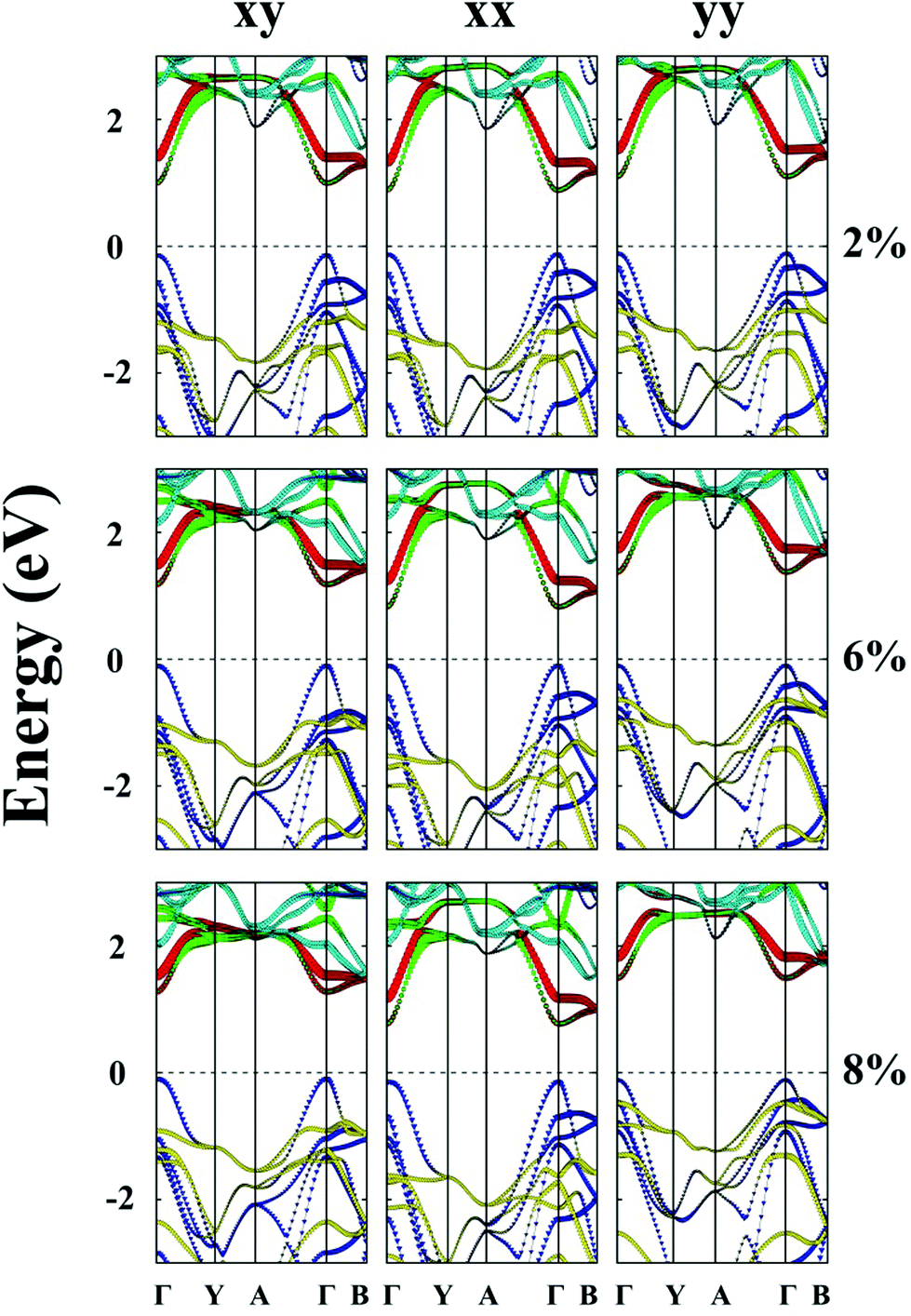 | ||
| Fig. 7 Computed band structures of the strained monolayered TiS3 subjected to the biaxial tensile strain both in the x and y directions (xy), the uniaxial tensile strain in the x direction (xx) or the y direction (yy). The red and green lines illustrate the dz2 and dx2−y2 orbitals of the Ti atom, respectively. The cyan lines represent the dxy, dyz and dxz orbitals of the Ti atom. The blue lines represent the px and py orbitals of the S atom, and the yellow lines show the pz orbital of the S atom. The dashed lines indicate the Fermi level. | ||
Bulk NbS3 is a triclinic structure with the space group of P1. As shown in Fig. 6(b) and ESI Fig. S8,† the unstrained NbS3 monolayer is a semiconductor with an indirect bandgap of 1.18 eV. The CBM, located on the Γ–B line, is mainly contributed by the dxz orbital of the Nb atom, while the VBM, located on the Y–A line, is mainly contributed by the dz2 and dx2−y2 orbitals of the Nb atom. The NbS3 monolayer retains its indirect bandgap, regardless of the biaxial and uniaxial tensile strain. Moreover, the strain can only change the bandgap modestly.
Conclusions
In conclusion, we present a comprehensive study of the effect of tensile strain on the electronic structures of transition-metal trichalcogenide monolayers, based on density functional theory computations. Our computations predict that MS3 and MSe3 (M = Ti, Zr, Hf, Nb) monolayers are all semiconductors, while MTe3 monolayers are metals. Both ZrS3 and HfS3 monolayers can undergo an indirect-to-direct bandgap transition with increasing tensile strain. The indirect bandgap of ZrSe3 and HfSe3 monolayers increases with the tensile strain, but the indirect character is retained in most cases. The ZrTe3 and HfTe3 monolayers can be transformed from a metal to semiconductor with an indirect bandgap at ε = 4% and ε = 6%, respectively. The TiS3 monolayer can retain its direct bandgap under either the biaxial or uniaxial strain, ranging from ε = 0% to 8%. The NbS3 monolayer retains its indirect bandgap, regardless of the tensile strain. Overall, the bandgaps of MX3 monolayers can be modulated from 0.68 eV to 2.34 eV at ε ≤ 8%.We note that as the atomic number of X increases from S to Te, the bandgap decreases significantly. For instance, the bandgap of ZrS3 is about 1.92 eV, whereas the bandgap of ZrSe3 is 0.92 eV. Note also that in their TMDC counterparts, the ZrS2 monolayer can transform from an indirect to a direct bandgap semiconductor when the uniaxial tensile strain is at ε = 8%.51 The TiS2 monolayer can also undergo the indirect-to-direct bandgap transition under the uniaxial strain of ε = 10%. In contrast, the ZrS3 and HfS3 monolayers can undergo the indirect-to-direct bandgap transition at a much lower tensile strain (ε = 2%). It seems that the indirect-to-direct bandgap transition can be induced more easily for the MX3 monolayers than for their MX2 counterparts by the tensile strain. The direct bandgap character and high bandgap tunability by strain as well as the availability of metallic and semiconducting properties of MTe3 (M = Hf and Zr) provide new opportunities for designing artificial layered structures for applications in optoelectronics and flexible electronics.
Acknowledgements
This work was supported in US by the National Science Foundation (NSF) through the Nebraska Materials Research Science and Engineering Center (MRSEC) (grant No. DMR-1420645) NSF, the UNL Nebraska Center for Energy Sciences Research, and the UNL Holland Computing Center. This study was supported in China by the NSFC (51472073), the program of the China Scholarship Council (No. 201408130035), the Foundation of Hebei Education Department (QN20131088), and the Peiyu Foundation of North China University of Science and Technology (GP201309).References
- A. Splendiani, L. Sun, Y. Zhang, T. Li, J. Kim, C. Chim, G. Galli and F. Wang, Nano Lett., 2010, 10, 1271–1275 CrossRef CAS PubMed.
- B. Radisavljevic, A. Radenovic, J. Brivio, V. Giacometti and A. Kis, Nat. Nanotechnol., 2011, 6, 147–150 CrossRef CAS PubMed.
- Y. Yoon, K. Ganapathi and S. Salahuddin, Nano Lett., 2011, 11, 3768–3773 CrossRef CAS PubMed.
- B. Radisavljevic, M. B. Whitwick and A. Kis, ACS Nano, 2011, 5, 9934–9938 CrossRef CAS PubMed.
- Y. Ma, Y. Dai, M. Guo, C. Niu, Y. Zhu and B. Huang, ACS Nano, 2012, 6, 1695–1701 CrossRef CAS PubMed.
- H. Wang, L. Yu, Y. Lee, Y. Shi, A. Hsu, M. L. Chin, L. Li, M. Dubey, J. Kong and T. Palacios, Nano Lett., 2012, 12, 4674–4680 CrossRef CAS PubMed.
- K. Kang, S. Xie, L. Huang, Y. Han, P. Y. Huang, K. F. Mak, C. Kim, D. Muller and J. Park, Nature, 2015, 520, 656–660 CrossRef CAS PubMed.
- Y. Li, Z. Zhou, S. Zhang and Z. Chen, J. Am. Chem. Soc., 2008, 130, 16739–16744 CrossRef CAS PubMed.
- Q. H. Wang, K. Kalantar-Zadeh, A. Kis, J. N. Coleman and M. S. Strano, Nat. Nanotechnol., 2012, 7, 699–712 CrossRef CAS PubMed.
- M. Chhowalla, H. S. Shin, G. Eda, L. Li, K. P. Loh and H. Zhang, Nat. Chem., 2013, 5, 263–275 CrossRef PubMed.
- K. F. Mak, C. Lee, J. Hone, J. Shan and T. F. Heinz, Phys. Rev. Lett., 2010, 105, 136805 CrossRef.
- V. Nicolosi, M. Chhowalla, M. G. Kanatzidis, M. S. Strano and J. N. Coleman, Science, 2013, 340, 1226419 CrossRef.
- J. N. Coleman, M. Lotya, A. O. Neill, S. D. Bergin, P. J. King, U. Khan, K. Young, A. Gaucher, S. De and R. J. Smith, et al. , Science, 2011, 331, 568–571 CrossRef CAS PubMed.
- R. J. Smith, P. J. King, M. Lotya, C. Wirtz, U. Khan, S. De, A. O'Neill, G. S. Duesberg, J. C. Grunlan and G. Moriarty, Adv. Mater., 2011, 23, 3944–3948 CrossRef CAS PubMed.
- L. Brattas and A. Kjekshus, Acta Chem. Scand., 1972, 26, 3441–3449 CrossRef CAS.
- S. Furuseth, L. Brattås and A. Kjekshus, Acta Chem. Scand., 1975, 29, 623–631 CrossRef.
- S. Kikkawa, N. Ogawa, M. Koizumi and Y. Onuki, J. Solid State Chem., 1982, 41, 315–322 CrossRef CAS.
- J. Rijnsdorp and F. Jellinek, J. Solid State Chem., 1978, 25, 325–328 CrossRef CAS.
- S. Kikkawa, M. Koizumi, S. Yamanaka, Y. Onuki and S. Tanuma, Phys. Status Solidi A, 1980, 61, K55–K57 CrossRef CAS PubMed.
- M. Hoesch, X. Cui, K. Shimada, C. Battaglia, S. Fujimori and H. Berger, Phys. Rev. B: Condens. Matter, 2009, 80, 75423 CrossRef.
- D. Pacilé, M. Papagno, M. Lavagnini, H. Berger, L. Degiorgi and M. Grioni, Phys. Rev. B: Condens. Matter, 2007, 76, 155406 CrossRef.
- P. Starowicz, C. Battaglia, F. Clerc, L. Despont, A. Prodan, H. van Midden, U. Szerer, A. Szytuła, M. G. Garnier and P. Aebi, J. Alloys Compd., 2007, 442, 268–271 CrossRef CAS PubMed.
- D. W. Bullett, J. Phys. C: Solid State Phys., 1979, 12, 277–281 CrossRef CAS.
- H. W. Myron, B. N. Harmon and F. S. Khumalo, J. Phys. Chem. Solids, 1981, 42, 263–267 CrossRef CAS.
- K. Stöwe and F. R. Wagner, J. Solid State Chem., 1998, 138, 160–168 CrossRef.
- C. Felser, E. W. Finckh, H. Kleinke, F. Rocker and W. Tremel, J. Mater. Chem., 1998, 8, 1787–1798 RSC.
- J. O. Island, M. Barawi, R. Biele, A. Almazán, J. M. Clamagirand, J. R. Ares, C. Sánchez, H. S. van der Zant, J. V. Álvarez and R. D'Agosta, Adv. Mater., 2015, 27, 2595–2601 CrossRef CAS PubMed.
- A. Lipatov, P. Wilson, M. Shekhirev, J. Teeter, R. Netusil and A. Sinitskii, Nanoscale, 2015, 7, 12291–12296 RSC.
- J. Dai and X. C. Zeng, Angew. Chem., Int. Ed., 2015, 54, 7572–7576 CrossRef CAS PubMed.
- Y. Jin, X. Li and J. L. Yang, Phys. Chem. Chem. Phys., 2015, 17, 18665–18669 RSC.
- J. O. Island, M. Buscema, M. Barawi, J. M. Clamagirand, J. R. Ares, C. Sánchez, I. J. Ferrer, G. A. Steele, H. S. van der Zant and A. Castellanos Gomez, Adv. Opt. Mater., 2014, 2, 641–645 CrossRef CAS PubMed.
- H. G. Grimmeiss, A. Rabenau, H. Hahn and P. Ness, Z. Elektrochem., 1961, 65, 776 CAS.
- D. W. Bullett, J. Solid State Chem., 1980, 33, 13–16 CrossRef CAS.
- G. Perluzzo, A. A. Lakhani and S. Jandl, Solid State Commun., 1980, 35, 301–304 CrossRef CAS.
- K. Patel, J. Prajapati, R. Vaidya and S. G. Patel, Bull. Mater. Sci., 2005, 28, 405–410 CrossRef CAS.
- K. Patel, J. Prajapati, R. Vaidya and S. G. Patel, Indian J. Phys., 2005, 79, 373 CAS.
- A. Zwick, M. A. Renucci and A. Kjekshus, J. Phys. C: Solid State Phys., 1980, 13, 5603 CrossRef CAS PubMed.
- J. A. Wilson, Phys. Rev. B: Condens. Matter, 1979, 19, 6456 CrossRef CAS.
- P. Johari and V. B. Shenoy, ACS Nano, 2012, 6, 5449–5456 CrossRef CAS PubMed.
- L. Kou, T. Frauenheim and C. Chen, J. Phys. Chem. Lett., 2013, 4, 1730–1736 CrossRef CAS PubMed.
- A. Castellanos-Gomez, R. Roldán, E. Cappelluti, M. Buscema, F. Guinea, H. S. van der Zant and G. A. Steele, Nano Lett., 2013, 13, 5361–5366 CrossRef CAS PubMed.
- H. J. Conley, B. Wang, J. I. Ziegler, R. F. Haglund Jr., S. T. Pantelides and K. I. Bolotin, Nano Lett., 2013, 13, 3626–3630 CrossRef CAS PubMed.
- Y. Y. Hui, X. Liu, W. Jie, N. Y. Chan, J. Hao, Y. Hsu, L. Li, W. Guo and S. P. Lau, ACS Nano, 2013, 7, 7126–7131 CrossRef CAS PubMed.
- K. He, C. Poole, K. F. Mak and J. Shan, Nano Lett., 2013, 13, 2931–2936 CrossRef CAS PubMed.
- C. R. Zhu, G. Wang, B. L. Liu, X. Marie, X. F. Qiao, X. Zhang, X. X. Wu, H. Fan, P. H. Tan, T. Amand and B. Urbaszek, Phys. Rev. B: Condens. Matter, 2013, 88, 121301 CrossRef.
- Q. Yue, J. Kang, Z. Shao, X. Zhang, S. Chang, G. Wang, S. Qin and J. Li, Phys. Lett. A, 2012, 376, 1166–1170 CrossRef CAS PubMed.
- A. Ramasubramaniam, D. Naveh and E. Towe, Phys. Rev. B: Condens. Matter, 2011, 84, 205325 CrossRef.
- Y. Zhou, Z. Wang, P. Yang, X. Zu, L. Yang, X. Sun and F. Gao, ACS Nano, 2012, 6, 9727–9736 CrossRef CAS PubMed.
- W. S. Yun, S. W. Han, S. C. Hong, I. G. Kim and J. D. Lee, Phys. Rev. B: Condens. Matter, 2012, 85, 033305 CrossRef.
- S. Bhattacharyya and A. K. Singh, Phys. Rev. B: Condens. Matter, 2012, 86, 075454 CrossRef.
- (a) P. Lu, X. J. Wu, W. L. Guo and X. C. Zeng, Phys. Chem. Chem. Phys., 2012, 14, 13035–13040 RSC; (b) H. Guo, N. Lu, L. Wang, X. Wu and X. C. Zeng, J. Phys. Chem. C, 2014, 118, 7242–7249 CrossRef CAS.
- N. Lu, H. Guo, L. Li, J. Dai, L. Wang, W. Mei, X. Wu and X. C. Zeng, Nanoscale, 2014, 6, 2879–2886 RSC.
- L. Kou, A. Du, C. Chen and T. Frauenheim, Nanoscale, 2014, 6, 5156 RSC.
- G. Kresse and J. Furthmüller, Phys. Rev. B: Condens. Matter, 1996, 54, 11169 CrossRef CAS.
- G. Kresse and D. Joubert, Phys. Rev. B: Condens. Matter, 1999, 59, 1758 CrossRef CAS.
- A. D. Becke, J. Chem. Phys., 1986, 84, 4524 CrossRef CAS PubMed.
- J. J. Klimeš, D. R. Bowler and A. Michaelides, J. Phys.: Condens. Matter, 2010, 22, 22201 CrossRef PubMed.
- J. Heyd, G. E. Scuseria and M. Ernzerhof, J. Chem. Phys., 2006, 124, 219906 CrossRef PubMed.
Footnote |
| † Electronic supplementary information (ESI) available. See DOI: 10.1039/c5nr04505c |
| This journal is © The Royal Society of Chemistry 2015 |